Note: Descriptions are shown in the official language in which they were submitted.
D/86 l 7 5 lZ~ 71 ~ 9
OPTICAL MOUSE
This invention relates to a cursor control device, otherwise known as an
optical mouse, for use with an interactive display oriented computer system to
provide movement for a visible cursor from position to position on a display screen
of such a system. The device includes an optically sensitive integrated circui-t chip
which is mounted into a printed wiring board in an inverted state which, in
conjunction with a straight optical path from a pattern pad, provides electricalsignals for use by subsequent digital circuitry.
BACKGROUND OF THE INVENTION
United States Patent 4,521,772, which issued on June 4, 1985, discloses a
cursor control deviGe, or "optical mouse" for use with an interactive display
oriented computer system to provide movement for a visible cursor from position to
position on a display screen of such a system. The device includes an IC ~integrated
circuit) chip that contains an optical sensor array and circuitry to bring aboutdetectable bit maps based upon a plurality of sensor cells making up the array: The
distinguishable bit maps are employed as a means for comparison to provide an
output indicative of the direction and amount of movement of the cursor control
device relative to an optical contrasting input to the array, the output being
employed as a means to move the visible cursor from position to position on a
display screen.
U. S. Patent 4,521,773, also issued on June 4, 1985, and assigned to the
same assignee as the previous patent and the present application, discloses an
imaging array which provides a plurality of distinguishable bit map images and
comprises an array of sensor cells capable of sensing radiation. The cells are
connected in a mannerto form distinguishable bit map images through a pattern ofcorrespondence among the cells. Each bit map image formed comprises a
combination of one or more cells indicative of detecting an image pixel within afield of array cells that have been non-indicative of such detection. The pattern of
correspondence may be one of inhibition of the operation of other cells in the array
or one of indication of operation to other cells in the array. Various patterns of
lZ1~717~
correspondence can be created among the cells creative
of bit map images. Bit map images may consist of
combinations of responsive cells within a field of non-
responsive cells in the array. For example, each bit
map image may comprise radiation responsive array cells
that have sensed a sufficient quantity of radiation
within a field of cells which have not sensed radiation
or have been inhibited from sensing radiation. On the
other hand, each bit map image may comprise cells that
have n~t sensed a sufficient quantity of radiation
within a field of cells that have sensed a sufficient
quantity of radiation. An application of the imaging
array is in an IC chip for a cursor control device or an
"optical mouse" for use with an interactive display
oriented computer system to provide movement for a
visible cursor from position to position on a display
screen of such a system.
The optical mouse as disclosed in these two patents
were operative as disclosed but found to have a
difficulty in the focus alignment for the light
reflected from the illuminated pattern pad to the
optical sensor array on the integrated circuit chip.
Improvement was necessary and work was undertaken to
create an optical mouse which did not include the folded
optics as disclosed in the two patents set forth above.
According to an aspect of the present invention, an
optical mouse is disclosed wherein the light source is
reflected off the optical pattern pad and is placed such
that a lens at a predetermined distance from the optical
pad focuses the light directly onto an inverted
integrated circuit mounted on and through a hole in a
printed wiring board, said integrated circuit being
housed in a clear plastic package. The path from the
lens to the integrated circuit package provides an
optical guide such that the distances from the pattern
pad to the lens, and from the lens to the optical sensor
in the integrated circuit, is fixed upon manufacture and
assembly without any further optical adjustment. The
1~71~9
inverted state of the integrated circuit chip allows a
fixed distance to be provided through the hole in the
printed wiring board rather than from above it as is
com~on in the prior art.
Other aspects of this invention are as follows:
A cursor control device, or optical mouse,
comprising:
a housing assembly including at least top, side and
bottom surfaces,
a printed wiring board mounted horizontally within
said housing,
a hole of predetermined size formed in said
printed wiring board,
integrated circuit mans mounted on one side of
said printed wiring board such that the active circuit
element thereof faces and is aligned with said hole,
optical guide means mounted in said hole and in
line with the active circuit element of ~aid integrated
circuit means,
lens means mounted at the end of said optical
guide means away from said active circuit element, and
lighting emitting means mounted adjacent said lens
means and said optical guide means to illuminate an area
a predetermined distance from said lens means, wherein
light reflected from said area is gathered and focussed
by said lens mean~ through said optical guide means onto
~aid activo c$rcuit element on said integrated circuit
means.
An improved optical mouse or like device, the
improvement comprising an integrated circuit package
including a housing, an active circuit slement mounted
in one surface of said housing on top of an integrated
circuit bonding plate, said housing also including
electric wires emanating from said bonding plate, said
electric wires being bent toward the surface of said
integrated circuit package containing said active
circuit element, to thereby allow said integrated
2a
r
~,,
.
circuit package to be ef fectively mounted in an
inverted position.
2b
~. ~,
.
lZ~'71 ~
DES~IPTION OF q~HE DRAWINGS
For a more complete understanding of the invention, reference may be
had to the following detailed description of the invention in conjunction with the
drawings wherein:
Figure 1a is the top view of a standard integrated circuit package
indicating pin placement and numbering thereof, while Figure lb is the pin
placement of the reversed, i.e., inverted, integrated circuit package and its pin
placement, and numbering as utilized in the present invention;
Figure 2a shows an integrated circuit wherein an optical sensor array is
placed in the integrated circuit and its normal pin placement and bending thereof
in relation to the optical sensor; while Figure 2b shows the reverse bend to an
integrated circuit with such an optical sensor array such that when the integrated
circuit is reversed and placed into a printed wiring board, the optical sensor array is
always at a predetermined fixed distance from the integrated circuit package to the
printed circuit board; and
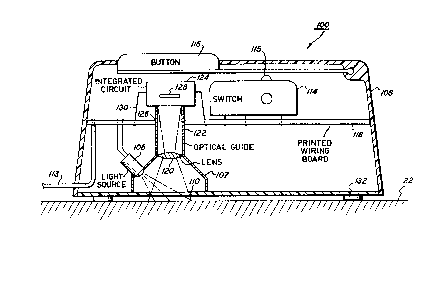
Figure 3 is a diagrammatic illustration of an optical mouse comprising
the present invention utilizing a lens, an optical guide, and a reverse bent, inverted
circuit package.
DETA!LED DESCRIPTION OF THE INVENTION
As is fully set forth in U. 5. Patents 4,S21,772 and 4,521,773, described
above, an optical mouse is a hand held cursor positioning unit with an overall
weight of approximately three ounces. Its outputs are digital signals related to its
positional change as it is moved over a pattern pad. Two or three or more buttonswitches can be provided on top of the optical mouse for the operator to make
functional selections. The optical mouse can interface with a host system via a
multi-wire cable assembly.
The optical mouse detects motion across a defined pattern pad by
means of optical sensors and converts this motion to x and y pulse train outputs.
The direction and speed of the motion is contained in the phase shift and frequency
of the output signals which is decoded and utilized in displaying the cursor on a
D/86175 12871,9
screen such as a cathode ray tube of a personal computer or workstation. At various
times, the push buttons which operate microswitches within the optical mouse
itself, can be utilized for certain functions on the surface of the screen of the
cathode ray tube. For example, depressing the left button when the cursor is below
and to the left of the left hand most letter of a word and the moving the mouse to
the right hand most letter of a word and then depressing the right hand button of
an optical mouse, can cause the highlighting of the word on the cathode ray screen
for deletion thereof, or changing of the font or the size of the letters within the
font, for example. Also, depression of one or the other switches can institute an
action on the screen such as a printing function or a deletion function when thecursor is over a predetermined place on the screen as may be necessary.
One disadvantage of the optical mouse set forth in the cited two
patents is the fact that a reflecting mirror comprising folded optics is necessary and
alignment thereof is required during the manufacture and assembly process. The
alignment of the optical system is labor intensive and therefore expensive, to say
nothing of the fact that folded mirror optics themselves must also be provided. The
present invention herein solves several problems in that when the entire unit isassembled during manufacture, no further mechanical or optical alignment is
necessary in order for all the optical equipment and components thereof to be intheir operational state.
Figure 3 of the present application shows a side view of the optical
mouse in accordance with the principles of the present invention. The optical
mouse 100 isshown to be covered by housing 108. This can be of molded plastic ofany of the well known types in the prior art. The major components o~ the optical
mouse are seen to be the button 116, which operates microswitch 114 via the
operating point 115. There could be two or even three or more of these buttons
and microswitches depending on the choice of the system and the required
operations. Normally, two or three microswitches and accompanying buttons are
utilized, as more than two or three becomes confusing to an operator and adds tothe complexity of the printed wiring board 118. The switch 114 would be mounted
in holes in the printed wiring board 118. Not shown on the printed wiring board
118 are other electrical components, such as resistors and capacitors and connectors
D/86175 :i287~179
which are necessary for the operation of the circuit but form no part of the present
invention. Light source 106 is included which is mounted in a housing 107. Lens 120
is shown installed in the optical guide 122 which fits through a hole 126 in theprinted wiring board 118. The light would shine upon the optical sensor array 128
as seen in Figure 3. The configuration of integrated circuit 124 will be discussed
hereinafter in relation to Figures 1 and 2.
In operation, therefore, the light source 106 would be utilized to shine
its light towards hole 110 in the bottom part of the cover 108 of the optical mouse
100. The light source 106 could be a light emitting diode which could emit light in
the visible or the infrared region depending upon the sensitivity of the opticalsensor array 128 mounted in the integrated circuit 124. There could be one, two, or
even three of these light emitting sources 106 mounted in housing 107 depending
upon the sensitivity'of the optical sensor array 128 and whether or not redundant
light sources are desired by the~ designer. Only one light source 106 is necessary,
however, for the principles of the present invention. As the light strikes the pattern
on pad surface 22, light and dark shadows are reflected from the surface, some of
which is focused by lens 120 through optical guide 122 onto the optical sensor array
128. The operation of the pattern on surface 22 and the meaning of the various
signals as detected thereby are fully covered in the two patents set forth above.
Because the light source 106 is mounted in housing 106, and lens 120 is situated at
the end of the optical guide 122, which extends through the hole 126 in printed
wiring board 118, and that the integrated circuit 124 fits as close to the optical
guide as can be made depending upon the length of the leads as bent in reverse
direction, the manufacture of the optical mouse is made simple by the fact that no
optical alignment or measurement is necessary subsequent to the assembly of the
parts of the present optical mouse.
The integrated circuit 124 is unique in its manufacture and its
implementation in the present invention. Figure la shows the pin numbering of a
standard integrated circuit package with the pin number 1 in the upper right hand
corner if viewed from the top. The alignment indentation is between pins 1 and 16.
It is in this top surface that prior art integrated circuits would have its optical sensor
array. However, the integrated circuit package of the present invention has been
D/86 175 12l~7~
reversed and inverted to allow the top surface to become the bottom surface so as
to allow for immediate alignment of the bottom surface thereof when the
integrated circuit package is mounted in its housing in the optical mouse. Figure 1 b
shows the inverted package pinout as would be the case for the integrated circuit of
the present invention. Since the pins are reversed in its inverted state, care must be
made to note where the pins are in the wiring process of the design of the printed
wiring board.
Figure 3 shows the integrated circuit 124 sitting on top of the optical
guidel22whichactsasthespacerfromthelensl20totheopticalsensorarray128.
However, the optical guide could be shorter above the hole 126 in the printed
wiring board which could allow for the pins of the integrated circuit to establish the
height above the board in which the optical sensor array sits, in that most
integrated circuits h'ave a wider dimension to the pins as they immediately extend
o~t from the body of the integrated circuit which narrows down to a less wide
dimension in the pins. Thus, if the holes in the printed circuit board are made only
to accommodate the narrow dimension of the pins of the integrated circuit, then
when the integrated circuit is positioned within the printed circuit or printed wiring
board, the shoulder of the place where the dimension changes from a narrow to
wide width of the pin can be used as the spacing aspect, assuming that the pins of
the integrated circuit package are bent accurately.
Figure 2a shows a normal, prior art, integrated circuit wherein the
active circuit chip element is on top of the integrated circuit bonding plate 134 in
the housing 124 and the leads are bent away from this operative surface. In Figure
2b is shown the integrated circuit of the present invention wherein the pins arebent toward the active optical sensor array 128 in the reverse position, and when
the entire integrated circuit is inverted such that the pins 130 are pointed
downward, the active optical sensor array surfaces also pointed downward and
would be positioned on the printed wiring board 118 as seen in Figure 3. In order to
allow for the active optical sensor array surface 128 to be accurately positioned
from the lens at the focal length thereof, the entire integrated circuit package can
be made of clear plastic, of the type which could allow for accurate placement and
distance from the lens to both the active optical sensor array and the surface of pad
D/861 75
lZ87179
22. Feet 132 in Figure 3 can provide for an accurate placement of the bottom
surface of housing 108 to be distanced from pad 122. The foot distance 132 from
the pad to the lens can be taken into account in the design of the system if it is
desired to have such feet 132.
It would be possible to incorporate lens 120 into the integrated circuit
package; however, this would require custom molds and special handling of the
new package shape. It is possible, however, as the compound used for encapulation
of the integrated circuit package 124 is optically clear plastic and is similar to that
used in prior art plastic lenses. In addition, higher orders of sophistication are
achievable in that the optical source, prisms, integrated lenses, and registration pins
and/or guides may also be incorporated into the custom plastic packages.
Since all,alignment is to the printed wiring board assembly t18, it
becomes feasible, and thus desirable, to make the total assembly of parts by
snapping them together rather than using screws and plastic welds. One of the
basic goals of the present invention was to create an inexpensive and accurate
optical assembly which would be compatible with automated assembly and testing.
As stated above, in prior art integrated circuit packages, the chip die is
on the top of the metal bonding plate. With the method of packaging as set forthherein, the chip die is mounted on the affected bottom of the plate, and since the
active area is on the chip die, the method of packaging will allow for:
1. automatic integrated circuit sensor to lens alignment;
2. in line ratherthan folded optical path;
3. single layer printed wiring board assembly may be used;
4. automatic integrated circuit insertion may be used;
5. single lens fixed focus;
6. simplified illumination; and
.
.
- ~; "' ~ . ~ ..
. ~ : . .
- '. -., : ~ -
.
- . . ,
. .: -, .
- : .
D/86175
12~71~9
7. reduced assembly steps and costs.
While the invention has been described with reference to specific
embodiments, it will be understood by those skilled in the art that various changes
may be made and equivalents may be substituted for elements thereof, without
departing from the true spirit and scope of the invention. In addition, many
modifications may be made without departing from the essential teachings of the
invention.
,.
:
.