Note: Descriptions are shown in the official language in which they were submitted.
` 3 ~7~
Brief DescriPtion of the Invention
A reversible resistance device has been conceived
wherein a normally non-conductive film is placed between two
conductive layers. Initially, the film is a dielectric or
insulator with high resistivity, but when exposed to certain
conditions, it will assume the properties of a conductor.
The normally non-conductive film includes metal particles
coated with a metal oxide metal layer, the coated particles
being received within a suitable binder to form a dielectric
layer. This dielectric layer is applied to the surface of a
conductor and a second film is disposed upon the first film.
The second film includes conductive particles being
impregnated in a high concentration within a binder so that
the second film is conductive. Another conductive surface
comes into contact with the second film. In this state, the
first film prevents current from flowing from the first
conductive surface to the second conductive surface. When
exposed to a high voltage, the metal particles are heated
and the dielectric strength of the oxide metal coated
particles will experience dielectric loss rendering the
parkicles conductive~ The metal particles will then flow
into contact with the first surface and the second film to
bring about an electrical connection between the two
conductive surfaces.
It its method aspect, the invention relates to a
method of producing a reversible resistant device, the steps
comprising: producing a normally non-conductive film by
rn/
74~
2a
dispersing within a first binder metal particles having
thereover a non-conductive coating which has the property of
breaking down when exposed to an electric force with up to
25~ of the diameter of the metal particles protruding from
the first binder; applying the normally non-conductive film
to a first conductive layer; applying a conductive film
comprising metal particles dispersed within a second binder
to the normally non-conductive film; and placing a second
conductive layer over the normally non-conductive film.
Brief Description of the Drawin~s
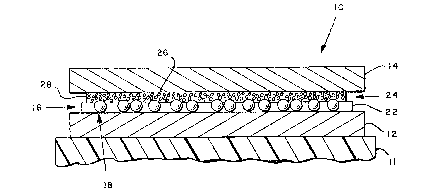
Figure 1 is a longitudinal view of a reversible
resistance device that incorporates features of the instant
invention;
Figure 2 is a partially cross sectional view of a
metal particle shown in Figure l; and
Figure 3 is a circuit diagram of a circuit used to
test the device shown in Figure 1.
rn/~
~ X~3'74~
Detailed Description of -the Preferred Embodiment
With reference to Figs. 1 and 2, a reversible resi~tance
device is shown generally at 10 that is suppor-ted on a
substrate 11. The reversible resistance device 10 includes
first and second conductive layers 12 and 14, respectively.
The Eirst conductive layer 12 is disposed upon the substrate
11. Normally these two conductive layers 12,14 would be part
of another device, apparatu~ or circuit and the like for
which temporary electrical isolation is desired. An example
of such a device would be a radio frequency ~RF) electronic
article surveillance ~EAS) tag and the two conductive
surfaces 12 and 14 would represent turns of a copper coil and
the substrate 11 would represent a paper or plastic outer
cover. Although not shown, in an RF EAS tag the upper
conductive layer would also have a plastic or paper cover
thereover. The use of the reversible resistant device 10
with such an EAS device will be explained hereinafter.
Applied to the surface of the first conductive layer 12
is a normally non-conductive film 16. This film 16 includes
a plurality of metal particles 18 having a metal oxide
coating 20 thereover. The metal particles 18 are embedded
within a binder 22 with the metal particles protruding
slightly beyond the binder 22. Applied to the top oE this
first film 16 is a second film 24 composed of metal flakes 2
in high concentration received within a binder 28. This
second conductive film 24 is in intimate contact with the
conductive surface 14 and receives the exposed portions of
the metal particles 18.
The break-down film 16 is composed of metallic particles
18 coated with a non-conductive material 20. Examples of
such particles are aluminum coa-ted with aluminum oxide and
copper coated with stearic acid. Aluminum has
characteristics that lends itself well to this applicationO
The coating of aluminum oxide is generally uniform and
relatively chemically inert. Such materials are commercially
available from Aluminum Company of America and identified as
~lcoa aluminum powder 1401 and from Aluminum Company oE
Canada and identified as Alcan*aluminum powder X-81. Such
* trade-mark
-- 3 --
-- ,,
l2~37~
particles 18 are added to a binder 22 .such as nitrocellulose
lacquer to form a smooth metallic dispersion. The particles
normally have a diameter of approximately 5-25 microns and
the oxide coating thereover will be approximately 5V
angstroms thick. When subjected to a relatively high voltage
or electromagnetic field, the oxide coating 20 will
experience a dielectric loss which will cause voltage
breakthrough and the metallic portion of the particles 18
will then become soft and fuse with the conductive Eilm 24
and the conductive layer 12. When this occurs, the Eirst
film 16 becomes conductLve. It has been determined
experimentally that the fusion resulting from exposure to a
high energy field and subsequent dielectric loss is more
extensive and stronger with aluminum particles when compared
to using coated copper particles unde~ the same
circumstances. The voltage required to bring about
dielectric loss is determined by the thickness and dielectric
strength of the oxide coating 20.
Preferably, the first film 16 is one particle layer deep
ln terms of metal particles 18. This has been found more
eEfective in shorting the film 16 when exposed to a high
voltage or electromagnetic field since only one coating (two
layers) of oxide needs to be overcome. Having the particles
18 extend slightly into the conductive film 24 also aids in
shorting of the aevice 10. If the binder 22 completely
covered the coated metal particles 18 a higher voltage would
be required for shorting because the binder 22 material
between the particles 18 and the film 24 would have to be
overcome.
The conductive film 24 is preferably made of a polymer
dispersed within a weak solvent of high volatility. ~y weak
solvent is meant those solvents which are characterized as
having a low or non-external polarization of molecules. In
addition, it is preferable that the conductive film 24 be a
dispersion of polymers as opposed to a solution. With this
combination, it has been found that the solution of the
conductive film 24 will not penetrate the binder 22 to bring
about premature electrical connection between the two layers
;
''
~L2~3~412
1~,14. Furthermore, being dispersed results in faster
evaporation rates of the solvents. More specifically,
diEfusion between the layers is reduced, thus, minimizing the
potential for premature shorting between the conductive layer
12 and the conductive film 24. The preferred conductive film
24 has a binder of acrylic dispersion within a solution of
VMP naptha filled with 65~ conductive material such as silver
flakes. The acrylic binder slightly blends with the break-
down film 16 to provide adhesion, but does not ully
penetrate the break-down film binder 22.
~ s stated previously, the metal particles 18 protrude
slightly beyond the binder 22. It has been found that
greater reliability is achieved through this expedience.
Preferably, the particles 18 will protrude approximately 20%
to 25~ of their diameter beyond the binder 22 and be
partially received within the conductive film 24.
With reference to Fig. 3, after the reversible
resistance device 10 has been Eabricated it is place~ within
the circuit 32 as a component thereof for the purpose oE
determining the voltage required to short the device. This
circuit 32 includes wiring 34 that connects the vario~s
components, a variable power supply 36, a resistor 38, a
capacitor 39 and a volt-ohm meter 40, to form a closed loop.
The reversible resistance device 10 is shunted into this loop
between the capacitor 39 and the volt-ohm meter 40. A
computer 41 is in electrical connection with the variable
power supply 36 and the volt-ohm meter 40. With this
circuit, one is able to make a determination of the voltage
required to break-down the resistant film 16. More
specifically, the device 10 was subjected to voltages in the
range of 0-50 volts. Initially, the computer ~1 directs the
variable power supply to provide a relatively small voltage
to the current, i.e., 5 volts. The computer 41 determines
the initial resistance and voltage of the reversible
resistance device 10. The computer 41 then causes the power
supply to increase the voltage and then determines the
voltage required to break-down the device 10 and measures the
~inal resistance after break-down. Ideally, the device 10
'~: ' 1,'
, i'l ' ' '
t
,:.
~ 37~
-
will maintain its dielectric state when 0-3 volts is applied.
A number of tests were conducted on the device 10 and it was
found that the dielectric 1059 of the film 16 did reach the
levels anticipated, i.e., in the range of 3-20 volts. It was
found that the break down voltage may be controlled by
varying the size of the particles 18 and the thickness of the
oxide coating 20 thereover.
Although the test was conducted using volta~e break-
down, it will be appreciated that the same applies when the
reversible resistance device 10 is placed in an
electromagnetic Eield. The dielectric strength oE the device
10 is overcome by the induced potential generated in the
device by the electromagnetic field so that a voltage i9
created and the switching results are achieved.
It will be appreciated that such a device 10 will be
useful in ~any fields. As indicated previously, the device
10 may be used to create a deactivatible ~F marker. The two
surfaces 12 and 14 would represent two turns of a copper coil
used in such a marker. Normally the two turns would be
isolated from one another so that the marker would be
responsive to an electromagnetic field to emit a responsive
pulse. In order to deactivate the marker, the marker would
be placed in a higher than normal electromagnetic field and
the device 10 would be rendered conductive, thereby shorting
out the coils 12,14. Other applications would include solid
state devices and integrated circuits wherein it would be
desirable to isolate two components under initial conditions,
but eventually provide a connection therebetween. ~n example
of this would be a write once memory.
~2~374~
-
EX~MPLE 1
Parts by Wei~ht
Breakdown film
Nitro cellulose lacquer 30
Aluminum ~Alcoa 1401) 1.2
Mixing procedure: Add aluminum powder to nitro
cellulose lacquer with adequate stirring to eEfect a
smooth metallie dispersion.
Conductive film
acryloid NAD-10
(40% in naptha) 10
silflake #237 metal powder 20
mixing procedure: Add metal powder to acrylic
dispersion with stirring
The breakdown film 16 is first applied to the first
conductive layer 12 by either spraying or painting. the
spraying may be either air press spraying or electrostatic
spraying. The painting may be either through flexographic or
gravure printing. After the breakdown film 16 is applied to
the conductive layer 12, it is dried either by remaining in
air for a suffieient period or by oven drying. The
conductive film 24 is applied to the breakdown film 16,
again, either by spraying or printing and the second
conductive layer 14 immediately applied thereto. The
conductive Eilm 24 is then dried to adhere both to the second
conductive layer 14 and the breakdown film 16.
-- 7 --
:
::.
- . .. .
: ':
- ~2S~741~:
-
~X~MP~ 2
Break-down film
acryloid ~3-48N
(g5~ in toluene) 30
Acatone 20
isopropanol3
Above solution 10
Aluminum Powder (Alean x81) 5
Conductive ~ilm
acryloid NAD~10
(40i in naptha) 10
silflake #237 metal powder 20
mixing procedure: Add metal powder to acrylic
dispersion with stirring
The same procedures may be used to Eabricate the
reversible resistant device as described in Example l.
. s . `;