Note: Descriptions are shown in the official language in which they were submitted.
~28~7~
PRINTING
The invention relates to printing, and in particular to a
method of screen printing on hard non-absorbent materials such as
glass, and screens for use in such a method.
An important application of screen printing is in the printing
of heater arrays comprising electrically conducting networks on
rear windows for motor vehicles, so that the surface of the window
can be heated to demist or de-ice the window. Such heater arrays
on the glass generally comprise an array of heating conductors
extending across the window between bus bars adjacent the lateral
edges of the glass.
The heater array may be printed on one surface of a glass pane
which is to form the vehicle window, before the pane is heated for
bending and toughening, using an ink which is a mixture of glass
frit, silver and binder material. rhe heater pattern is screen
printed using a screen in which the required pattern is defined by
a coating on the screen surface, and is fired on to khe glass
surface when the glass sheet is heated for bending and toughening;
the binder ls generally burnt off during the firing process. The
ink may include a resin which is curable by ultraviolet light so
that the printed heater array can be cured by brief exposure to
ultra-violet light before handling.
~ X ~r7 7 7 z
It is desirable to be able to increase the thickness of the
printed ink pattern at one or more locations, for example to
selectively incrQase the conductance of parts of the pattern such
as the ous bars, or to provide a thlcker conductive layer where an
electric connector is to be soldered on to a bus bar. It is
possible to increase the thickness of the pattern in selected
locations by printing a second layer of ink over those pattern
areas in which the increased thickness is required using an
appropriately patterned screen. However, it is difficult in
practice to achieve the necessary registration between the two
prints, and, because of the need for a second pass through a
printing process, additional production costs are incurred.
British patent specification GB 1 262 176 relates to the
screen printing of electronic circuits using metal screens in place
of woven fabric screens. The required pattern is printed through
openings in the screen, which thus acts as a stencil for the
pattern. In order to print pattern areas of varying thickness, it
is proposed to incorporate a metal mesh in the openings where an
ink layer of reduced thickness is required. This mesh occupies a
part of the volume which would otherwise be available for the paste
or ink being printed on the substrate, and leads to a reduction in
the thickness of the pattern printed in such areas.
European patent specification EP O 193 464 A2 refers to two
methods for selectively increasing the thickness of certain areas
of a conductive pattern to be used as a heater array on a vehicle
window. In the first method, said to be described in DE-OS 32 31
382, a screen is used which has thicker threads, for example
,
~L~37 ~77~
thicker weft threads, in those areas in which a thicker conductlve
layer is required. In the second method, the subject of EP O 193
464 A2, a screen is used which has a coarser mesh in those areas in
which a thicker conductive layer is required; this coarser mesh is
achieved by omittlng alternate weft threads from the screen
material in those areas.
The two methods referred to in the European patent
specification both suffer from the disadvantage that all parts of
the patterns in the areas in which the weft (or warp) fibres are
modified or omitted are increased in thickness. It is desirable to
have a more versatile method in which any desired areas, or all
areas of the printed pattern can be increased in thickness.
In British patent specification GB 1 307 535, this problem is
avoided by using a silk screen on which a patterned emulsion
coating defining the pattern to be printed is of increased
thickness in areas surrounding and defining the areas in which
increased ink thickness is required. However~ in practice this
method has not proved very successful, especially when printing
wide bands of ink, such as the bus bars of heater arrays on vehicle
backlights.
It has now been found that the thickness of a patterned ink
layer screen printed on a hard non~absorbent substrate can be
increased in required locations by providing local support between
the screen surface and the substrate in those areas in which
increased thickness is required.
Surprisingly, it is found that the use of local support
between the screen surface and the substrate leads (provided the
77~
support is not too bulky) -to increased ink retent:ion :in those
areas, despite the eEEect of said support in occupy:ing vo:Lume
which would otherwise be available Eor occupation by the ink.
According to the present invention, -there :is provided
a method of screen printing a patterned ink layer on a hard
non-absorbent substrate using a screen with a patterned coating
on its surface facing the substrate, the method comprising the
steps of providing between the screen surface and the subs-trate
local support distributed over at least one area in which a
patterned ink layer of increased thickness is required thereby
enhancing ink retention in the at least one area, the at least
one area comprising only a part of -the patterned ink layer
printed by the screen, applying ink to the screen and printing
the patterned ink layer on the substrate through the screen,
whereby the ink layer in the at least one area is thicker than
in another area of the ink layer.
The method of the invention is especially useful for
printing patterns of varying thickness.
The local support may be provided by one or more
patches of screen material adhered to the coated surface of the
screen, or by one or more arrays of small spaced spots of
coating on the screen, in those areas in which a patterned ink
layer of increased thickness is required.
When one or more patches or screen material is used,
any such patch is preferably of coarser mesh than the screen.
When an array of small spaced spots of coating on the
screen is used, it is convenient to use a uniform array. The
shape of the spots is not critical, bu-t round spots are
preferred. The sma:Ll spaced spots oE coating may occupy about
10% of the area in whieh the ink layer oE increased th:ic)crless
is required, and preEerably occupy l~, to l56, espec:ia:l1y 2.5%
to 106, of said area. The pa-t-terned coating :in any area of the
sereen will usualLy be a-t least as thick as -the coating of ink
required in that area. In the screen areas surrounding and
defining the area(s) in which an ink layer of increased
thiekness is required i.e. the areas surrounding and defining
the area(s) of arrays of small spaced spots, the coating on the
screen will usually have a thickness of over 30 microns, and
preferably a thickness in the range 30 to 70 microns. It is
not neeessary for the coating to be as thielc in other areas,
and sueh areas will usually have a coating thielcness in the
range 5 to 15 microns, preferably 7 to 12 mierons.
The small spaeed spots of coating may be formed of
the same material as the patterned eoating and be of a height
equal to the thickness of said coating, which will usually be
at least 30 microns in the area(s) immediately surrounding the
area(s) in whieh a patterned ink layer of inereased thiekness
is required. The spots may be printed as deseribed hereafter
by including appropriate half tone areas in the ar-twork used in
produeing the screen.
The method of the present invention is especially
useful for printing a pattern in -the form of a heating array on
a glass pane for use as a vehiele window. In one embodiment,
the pattern eomprises an array of heating eonduetors extending
between bus bars, and loeal suppor-t is provided in those areas
of the bus bars where the eonneetors for eonductors supplying
the heating eurrent are to be attaehed.
~ `~
7~
According to a further aspect of -the invention, there
is provided a printing screen with a patterned coating on at
least one surface thereof for forming a patterned :ink layer, a
patch of screen material adhered to the screen wi-thin the
coating pattern so as -to occupy a-t least one d:iscr~ete ared of
-the pattern at which the thickness of the ink layer is to be
increased, the patch occupying less -than the entire area of the
coating pattern so -that an area of the coating pattern which is
free of the patch produces an ink layer of less thickness than
the increased thickness.
According to a still further aspect of -the invention,
there is provided a printing screen with a patterned coating on
at least one surface thereof including an array of small spaced
spots of coating on the screen surface in each of one or more
areas in which a patterned ink layer of increased thickness is
required, the thickness of the coating in the areas surrounding
and defining the area(s) in which an ink layer of increased
thickness is required being greater than the thickness of the
coating in other areas. Preferably the thickness of the
coating in the areas surrounding and defining the area(s) in
which an ink layer of increased thickness is required is at
least 30 microns. The coa-ting in other areas preferably has a
thickness in the range 5 to 15 microns.
The application of the inven-tion to the printing of a
heating array on a vehicle window in which the b~ls bars are of
increased thickness in those areas in which connectors are to
be attached will now be described by way of example, and with
reference to the accompanying drawings, in which:-
Figure l is a view oE the inside surface of a vehiclerear window with an obscuration band around its periphery and a
heater array,
-- 6
gL~8~7"772
Figure 2 is an enlarged perspecti.ve view, p~rtl.y in
section, showing the region of one of -the bus bars oE the
heater array with a connector attached,
Figure 3a is a diagrammatic view of the ar-twork used
for producing a prin-ting screen :Eor printing -the hea-ter array
onto the glass surface,
Figure 3b is an enlarged view of the detail shown a,t
b in Figure 3a,
Figures 4a to 4c illustrate the screen printing of a
bus bar at the section A-A of Figure 2,
Figures 5a to 5c illustrate the printing of a thicker
part of the bus bar at the section B-B of Figure 2, and
Figures 6a to 6c illustrate an alternative way of
printing a thicker area of the hus bar at the section B-B of
Figure 2,
Figure 7 is a diagrammatic plan view of a printing
screen in accordance with the invention for printing a heater
array with extended bus bars,
Figure 8 is a section on the line C-C in Figure 7.
In the drawings the dimensions of some parts are
greatly exaggerated for the sake of clarity.
.~
~ 37 ~77~
Figure 1 illustrates a vehicle window comprising a glass pane
1 which has a black obscuration band 2 printed around the periphery
of the inner surface of the pane using a black paint which is then
cured in known manner. Printed onto the inner surface of the glass
pane9 and on top of the obscuration band, is a heater array
comprising electrical resistance heating conductors 3 which extend
between bus bars 4. The heater array is screen printed on to the
glass surface ~hich already carries the obscuration band using a
ceramic inkO The ink is a mixture of glass frit, silver and a
binder material and may include a proportion of ultra-violet
curable resin. The layout of the heater array is designed so that
the bus bars 4 are screen printed on top of the obscuration band 2
as shown more clearly in Figure 2.
A T-shaped copper connector 5 is soldered to each of the bus
bars and in the particular embodiment illustrated in Figure 2 each
connector 5 has two feet 6 which are connected by a bridge from
which the connection tab extends.
The heater array 3,4 is screen printed onto the glass surface
using ceramic ink and is then fired onto the glass surface when the
2C glass sheet is heated, for example to a temperature in the range
580C to 670C, before being bent to shape and then toughened using
streams of cooling air.
Figures 3a and 3b illustrate diagrarnmatically the artwork used
for the production of a printing screen for carrying out the method
of the invention. The heater array of heating conductors 3' and
bus bars 4' are drawn in solid black on a transparent film, and in
-- 8 --
77~
the local areas 7' where connectors are to be soldered to the bus
bars, areas of half tone transparency ~, shown more clearly irl
Figure 3b, are incorporated into the artwork. Typically the half
tone transparencies ~ employed are such that 90~ of the area of
each transparency 8 is solid black defining a uniform array of
spaced clear spots.
The printing screen may be prepared by coating a suitable
screen and forming a pattern in the coating~ Usually a screen
which has 100 or 120 threads per centimetre is cleaned and
sufficient layers of wet photosensitive emulsion applied and dried
to provide an emulsion layer approximately 10 microns thick over
one surface of the screen. One or more layers of emulsion may also
be applied and dried on the other surface of the screen as is known
in the art. Further coatings of emulsion are successively applied
and dried to said one surface of the screen in the areas
surrounding and defining the areas in which an ink layer of
increased thickness is required to provide a layer of dried
emulsion coating which may, for example, be approximately 40
to 60 microns thick in such areas.
The artwork of Figure 3a is then placed against the coating of
dried emulsion and secured in position with transparent tape. The
transparency and screen combination is placed on a glass plate with
the transparency between the screen and the plate. The screen is
then covered and vacuum applied to remove air and ensure good flat
contact between the glass, the transparency and the screen. A
light source is then s~itched on behind the glass plate for the
required exposure time. The screen is separated from the artwork
~2~
and the glass plate and washed with warm water sprays to d~ssolve
away the non-exposetl areas of the emulsion, that is, to dissolve
away the heater array pattern including 90% of the half tone areas
71l leaving a patterned coating 10 (see Figures 4a and 5a) of
photocured emulsion on the screen.
The printing screen is then placed on the glass pane 1 with
the emulsion coated side in contact with the glass pane 1 and the
obscuration band 2. This is illustrated in Figure 4a which shows a
section through the woven screen 9 carrying coating 10 in which
there is an aperture 11 corresponding to the width of a bus bar in
the region of a thinner part of the bus bar, for example at the
section A-A in Figure 2. Section A-A is close to an area in which
an ink layer of increased thickness is required, and the thickness
of the coating 10 on the screen A A is approximately 40 microns.
Wet ceramic ink 12 is then spread on to the screen 9 during the
first passage of a squeegee blade 13 across the screen. This first
passage of the squeegee 13 forces ink 12 through the screen where
there is any aperture in the coating 10 such as the bus bar
aperture 11. On the return run of the squeegee back across the
screen the retained ink is forced into the aperture 11 and on to
the surface of the obscuration band 2 on the glass.
Where the thinner parts of the bus bar are being printed the
first run of the squeegee blade 13 depresses the unsupporked parts
of the screen 9 downwardly towards the glass surface. That is, in
Figure 4a, the run of the squeegee across the aperture 11 will
depress the screen 9 somewhat into that aperture thereby limiting
- 10 -
~ 8 7 ~
the whole height for the retention of ink for printing on to the
obscuration band. Figures ~b and ~c illustrate how the hel~ht of
ink 14 which passes through the mesh of the screen 9 (shown In
Figure 4b) is depressed so that at the end of the printing
process, when the ink has run together to form a printed layer 15
on the glass surface, only a thin layer (shown in Figure ~c) is
produced. For example in the embodiment illustrated the thickness
of the printed ink layer at the section A-A of the printed bus bar
is 22 microns, while the local thickness of the coating 10 on the
screen is 40 microns and the screen itself is 65 microns thick.
In the area of the printing screen which is to print the
thicker area 7 of the bus bar, the emulsion coating, as indicated
in Figure 5a, includes a half tone array oF solid spots 16 which
are distributed regularly over the whole local area which produces
the thicker area 7 of the bus bar. These spots 16 constitute 10%
of the area and provide, in effect, supports for the screen 9 in
the bus bar aperture 11.
The effect of this modification of the printing screen, to
incorporate half tone areas in the coating where the connectors are
to be soldered to the bus bars, is to enhance the retention of the
ceramic ink within those areas during the first pass of the
squeegee blade 13 across the screen because the screen is not
substantially depressed towards the glass surface, so that after
the second passage of the squeegee a deeper quantity 17 (Figure 5b)
of the ceramic ink is retained in the aperture 11 which runs to
form a thicker printed area as indicated at 18 (Figure 5c). The
- 11 -
377~
depth of the ink 18 which is thereby printed onto the surface of
the obscuration band 2 to form one of the thicker areas 7 oP the
bus bar may be bwice the thickness of the ink 15 printed on the
thinner parts of the bus bar, for example about 40 microns thick.
Thus, in the embodiment lllustrated, the thickness of ink in the
area of increased thickness corresponding to the half tone areas is
36 microns, while the local thickness of the coating on the screen
is 40 microns and the screen itself is 65 microns thick.
It has been found that a 50% increase in the thickness of each
bus bar in the areas where the connectors are to be soldered is
sufficient, although a thickness increase of 100~ can be achieved
using the half tone pattern areas provided the emulsion coating is
sufficiently thick in the areas surrounding and defining the half
tone areas.
The enhancement of ink retention by the local support provided
the spots 16 given at each of the dotted areas an increased
presence of silver in the thicker area of ink 18 so that even
though there may be absorption of xilver from the fired ink into
the obscuration band, there remains sufficient silver in each of
the thicker areas 7 to ensure a satisfactory soldered joint with
the T-shaped connector.
Figure 6a illustrates an alternative way of enhancing the
retention of ceramic ink to produce the thickened areas 7. The
artwork for producing the printing screen does not have any special
areas of the bus bars 4' as in Figure 3, the drawing of the bus
bars being continuous and solid. A patch 20 of screen material of
- 12 -
~2~7~2
coarser mesh cut to the size of the thicker areas 7 is adhered to
the screen 9 in areas of the screen which define the areas where
connectors are to be soldered to the bus bars. The patches 20 may
be secured to the screen by means of a suitable adhesive before the
emulsion is applied but more suitably are placed in position after
the emulsion has been applied and while it is still wet, and
additional emulsion used to cover the patches. After exposure and
washing of the screen the patches 20 are in position in the
emulsion coating 10 as indicated in Figure 6a. During the passages
of the squeegee 13 across the screen each of the patches 20 serves
to support the screen 9 and to provide a coarser mesh for enhanced
retention of ceramic ink so that a depth of ceramic ink 17 (Figure
6b) is retained giving a quantity of ink 17 in those areas
sufficient to produce, when fired, the thicker areas 7 of the bus
1~ bar. The depth of ink 17 collapses to a thickness of 18 as
indicated in Figure 6c which is comparable to the thickness
produced by printing through the half tone areas in Figure Sa.
The method of the invention is also useful for printing heated
backlights with extended bus bars which are sometimes employed, not
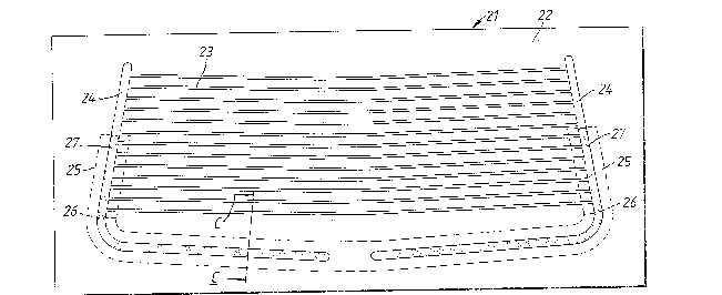
only as a heater, but also as an antenna for a radio. Figures 7
and 8 illustrate a silk screen in accordance with the invention for
printing a heated backlight of this kind. In these Figures, a silk
screen 21 carries a patterned layer of dried emulsion 22 defining
the pattern for two opposed L-shaped bus bars 24 and a plurality of
parallel heating conductors 23 extending between the bus bars.
When such L shaped bus bars are employed, it is desirable, to
- 13 -
87~7~
avoid excessive pcwer dissipation in the bus bars, to provlde
thickened bus bars, at least in the sections of the bus bars
extending from the adjacent ends thereof (where terminals are
attached for the supply of heating current and derivation of a
radio signal) to half-way up the array of heating conductors. To
achieve this increased thickness, the screen is initially coated
uniformly with a number of layers of emulsion which are
successively applied and dried, in known manner, over the whole
area of the screen. A further series of emulsion layers are then
applied and dried, using appropriate masks to contain the emulsion,
to the screen area 25, having the shape of an inverted channel
section and defined by the broken line 26 in Figure 7. It is
desirable to provide a gradual transition between the thinner and
thicker emulsion layers (see Figure 8~ and this may be achieved by,
for example, using a series of masks with progressively reduced
coating areas to apply the successive layers of emulsion to area
25, and dissolving away, for example with water, any resulting
sharp corners. The pattern in the emulsion is then prepared using
appropriate art work, using half tone transparencies (as described
above with reference to Figures 3a and 3b) in the parts of the bus
bars within area 25. Again, the half tone transparency employed is
typically such that about 90% of the area of each transparency in
solid black defines a regular array of spaced clear spots. The
spaced clear spots result in the production of a corresponding
array, designated 27, of solid spots or columns over the area of
the screen which is to be used to print the thicker areas of the
L-shaped bus bars.
- 14 -
~`` ~L~8P~7 Z
Using a screen as described above, a heated backlight suitable
for use as a radio antenna without unacceptable power dissipation,
can be printed in a sinale printing stage. This compares
favourably with the prior art process9 which required overprinting
of the thickened areas of the bus bars, involving a second pass
down the printing line.
The invention thus provides a versatile and precise solution
to the problem of printing a pattern of increased thickness in
selected local areas, without the need for overprinting with a
second layer of ink. Overprinting using the method of the
invention enables especially thick patterned layers to be achieved.
- 15