Note: Descriptions are shown in the official language in which they were submitted.
3~3~
MULTIPLE JUNCTI0N DEVICE
This Application claims the priority of Japanese
149,832/87, filed June 16, 1987 and Japanese 154,066/87,
filed June lg, 1987.
The present invention is directed to an improved
form of junction box, more specifically, a device ~or
making electrical contact within a circuit by means of an
integrated unit. The device of the present invention is
particularly adapted for use in the automotive field and
has the ability to provide multiple contacts in a small
volume.
THE PRIOR ART
In circuitry making use of electrical wires, the
connections are usually made by means of certain devices
which mate with one another and, if desired, are suitably
releasable as needed. Such devices have been in common
use in connection with automobiles but, as the complexity
of the wiring has increased, a need has arisen for a
connecting device which will be capable of handling a
large number of individual connections in a very limited
volume. Such devices provide a wiring board of one or
more layers with an insulating layer of plastic
therebetween. The necessary electrical terminals are, of
course, also provided, along with a plastic housing or
case.
~ 7 ~
Such devices frequently place the insulated
wiring on the underside o~ the insulation board with a
connection tab attached thereto. The lower tip oE the
connection tab grips the wire at a predetermined point and
- 5 the other ends of the tabs are aligned rather precisely in
order to be complementary to another mating connector.
The usual connection tab includes a relatively
wide throat portion at the end adjacent the wires and it
: . .,
is intended that the wire conductor be squeezed against
. . .
the throat so that its insulation is penetrated thereby
- and contact made therewith. It is, therefore, necessary
in the prior art devices to leave substantial space
between the connection tabs to provlde for the foregoing
contact and to leave sufficient room for the wires being
connected. As a result~ the prior art devices, especially
if they are to handle a substantial plurality of wires,
are excessively bulky.
SUMMARY OF T~-IE PRESENT INVENTION
It is an object of the present invention to
produce a junction device having multiple layers capable
of making connections between a large number of individual
~ires. It is also among the objects of the present
invention to provide a device of the foregoing capability
in a small volu~e. It IS further an object of the present
. ~ . .
78~3
invention to utilize a connection tab haviny a throat for
contact with the wire at one end and a matiny member for
use wi-th another electrical connector at the o-ther end.
In achleving the foregoing objects, there is pro-
vided a connection tab for making contact with an electric
wire at a wire contact and having a connecting end remote
from the wire contact, the connecting end being complementary
to and matable with an external connector and being offset
from the wire contact in a direction longitudinal of the
electric wire, perpendicular to the electric wire, or both.
The wire contact is made up of a pair of prongs
having a throat therebetween which preferably tapers away
from its opening. It is also preferable that at least one
edge of the throat constitute a cutting blade which is adapted
to penetrate insulation on the wire and make electrical con-
tact therewith.
The Invention also comprises a junction device
having a first wiring board with one or more connection areas
mounted thereon. There is at least one electrical wire be-
neath the first wiring board and a corresponding number ofthe aforesaid connection tabs. Usually, there i.s a plurali-ty
of such wires, each of which is to be connected. In a pre-
ferred form of the device, the wire contacts of the tabs
extend through the first board and are retained within grooves
in an outer casing.
~3
- ., , , :
, , ' ' ' : ' .
.
J3~B~7~
In a more complex form of the device, there is at
least a second wiring board beneath the first wiring board
and insulated therefrom. In addition to the wiring
beneath the first board, there is wiring beneath the
second board. Further connection tabs are provided which
extend into the connection areas and pass through ~he
first board and the second board to extend into the space
between the second board and the outer casing. In this
way, it is possible to compress a substantial number of
connectors in a small unit. Here, too, the casing is - -
preferably grooved to receive the ends of the tabs. ~ ;
The nature of the connection tabs also assists in
achieving this desired result. Such tabs preferably have
a generally flatened shape and the wire contact end is
offset from the connecting end. Such offset can be
longitudinally of the wire being held, perpendicular
thereto, or both. This permits adjusting the positions of
the members gripping the wire and the wires themselves to
avoid unwanted interference, while, at the same time,
maintaining the connecting ends of the tabs in appropriate
alignment for mating with another connector.
The nature of the wires used is not particularly
critical; e.g. they can be single conductor or twisted,
with or without insulation. However, the device is
particularly intended for use with insulated, single
conductor, hard copper wiring.
~ ~r~ 9~3
BRIEF DESCRIPTION OF THE DRAWINGS
In the accompanying drawings, constituting a part
hereof, and in which like reference characters indicate
like parts,
: 5 Figure 1 is an exploded view, partly schematic,
of a single-layered device according to
: the present invention;
Figure 2 is a view, similar to that of Figure 1,
of a form of the device hav.ing two
layers;
Figure 3 is an enlarged diagrammatical view of a
; tab according to the present invention
which is ofset in a direction
perpendicular to the wire;
Figure 4 is a view similar to that of Figure 3
wherein the connecting end is of~set in
a direction both longitudinal of and ~ :
perpéndicular to the wire; :
Figures ~:
5 to 7 are schematic views of fragments of
various wiring boards or panels
according to the presen-t invention;
~..2l~7~3~3
Figure 8 is a cross sec-tional view of an
assembled device according to the
present invention; and
Figure 9 is a view of the underside of the
wiring board of Figure 1.
DETAILED DESCRIPTION OF THE INVENTION
~'~
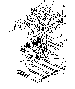
Referring specifically to Figure 1, first wiring
board 1 carries a plurality of connecting areas 7
thereon. A plurality of connection tabs 2 is also -
provided. Electrical wires 3 are located on the underside
of board 1 and contact is made therewith through tabs 2,
and bottom casing 4 with grooves 10 completes the device.
,''
A multi layered device is shown in Figure 2. In
addition to first wiring board 1, second wiring board 6 i5
located between casing 4 and first wiring board 1.
Additional wires 3 are held on the underside of board 6,
~n a manner similar to the embodiment of Figure 1~ Tabs 2
extend from wires 3 through boards 6 and 1 to project into
connec-ting areas 7. The opposite ends of tabs 2 project
partially into grooves 10 in casing 4.
37~
The nature of the tabs is shown more clearly in
Figures 3 and 4. Tabs 2 comprise connecting end 2a and a
pair of prongs 2b. Prongs 2b are spaced apart to form
;~` throat 2c through which wire 3 is inserted. Wire 3 is in
- 5 the usual form having center conductor 3a and insulating
layer 3b.
. ,
As is shown in Figure 3, connecting end 2a is
~- offset from prongs 2b and throat 2c in a direction
perpendicular to wire 3. In Figure 4, a similar device is
~" 10 shown with prong 2b and throat 2c offset in a direction
longitudinal of and perpendicular to wire 3. This is
accomplished by providing bend 2d in tab 2.
.,
In the device of Figures 5 to 7, the wire
contacts of tab 2 are staggered in their arrangement in
- 15 the device. However, the connecting ends, due to the
offsets of tabs 2, are fully aligned so that they are
adapted to mate with another connector (not shown~.
,
Referring more particularly to Figure 8, wire
contact 2b located in wiring board 6 is held on insulation
~ board 9 through slit 8. Wire contact 2b used for wiring
board 1 also passes through insulation board 9 and rests
on bottom casing 4.
,''
,
~ .
~ ~3~ ~ 9~.~
Figure 9 is a fragmentary, schematic bottom view
of wiring board 1. Wires 3 are aligned on one axis and
slits 8 are aligned on another axis in order to best
achieve the benefits of the present invention. Thus, by
the various offsets of the connection tabs, it is possible
to locate the wires more efficiently without giving up the
ability to have the connecting ends of the ~abs in an
appropriate simple alignment for engagement with another
connector.
Although only a limited number of specific
embodiments o~ the present invention have been expressly
. disclosed, it is, nonetheless, to be broadly construed and
not to be limited except by the character of the claims
appended hereto.