Note: Descriptions are shown in the official language in which they were submitted.
~ ~375~0~
.
LOSS OF OPTICAL INPUT CIRCUIT
CROSS^REFERENCE TO RELATED APPLICATIONS
The present application is related to the following co-
pending Canadian Patent Applications all having a common assignee:
Serial No. 552,253, titled, "OPTICAL DETECTOR CIRCUIT", now
abandoned;
Serial No. 552,251-0, titlèd, "LASER DRIVER CIRCUIT";
Serial No. 555,255-2, titled, "LASER DC BIAS CONTROLLER";
Serial No. 552,254-4, titled, ~LASER TEMPERATURE
CONTROLLER";
BACKGROUND OF T~IE INVENTION
This invention relates in general to fiber-optic
receiver/transmitter arrangements and more specifically to a novel loss
of optical input circuit for a fiber-optic receiver.
Fiber-optic receivers and transmitters or fiber-optic
interface units are used in modern telecommunications and data
transmission systems between an optical fiber transmission line and
electronic digital equipment. The fiber-optic transmitter receives
electrical signals from the electronic equipment representing the data
to be transmitted. The transmitter then converts the data to light
pulses which are coupled to an optical fiber transmission line. The
fiber-optic receiver receives light pulses representing the transmitted
data from an optical fiber transmlssion line and converts the light
pulses to electrical signals which are sent to and processed by the
electronic digital equipment. These systems work in very high
transmission rates from 145Mbs to 2400Mbs (Megabits per second).
Transmission of data or other signals along optical fibe~
transmission lines have advantage in the fact that light rays are almost
immune to electromagnetic interference such as sparks, lightening,
crosstalk and other interference which may be induced into the
transmission line.
It is advantageous in fiber-optic receivers of the type
discussed above to ascertain if a reliable optical input signal is
.
, I :, : ;,, . ;
. :
: . :..
. .
~ ~;;3~0~
.
being received. The fiber-optic recelver then can send warning
alarms to a system controller notifying that a problem exists on
the transmission line.
It therefore becomes an ob~ect of the present invention
to disclose a novel loss of optical input signal detector which
can detect the loss of the optical input signal and signal a
system controller of the problem.
SUMMARY OF THE INVENTION
In accomplishing the object of the present invention
there is provided a fiber-optic receiver which includes an optical
detector for receiving an optical signal, and a loss of signal
generating circuit for developing a signal voltage when the
optical input drops below a preset threshold.
The loss of optical input detector of the present
invention includes voltage follower means connected to the loss
signal generating circuit. The voltage follower passes to the
detector circuit the signal voltage from the loss signal
generating circuit.
Comparator means comprising first and second switching
devices has the first switching device connected to the voltage
follower means. The second switching dsvice is connected to a
reference voltage source. The second switching device produces a
positive voltage signal in responsa to the application of the
signal voltage to the first switching device from the voltage
~5 follower means, when the applied voltage signal is greater than
the reference voltage.
Alarm signal generating means connected to the second
switching device provides a visual alarm indication and an alarm
signal to a controller interface indicating the loss of the
optical input signal. The alarms are triggered by the applied
positive voltage signal from the comparator means second switching
device.
A BRIEF DESCRIPTION OF T~IE DRAWINGS
A better understanding of the invention may be had from
the consideration of the following detailed description ta~en in
conjunction with the accompanying drawings in which:
: , ;.. :-.. ;
. .
Fig. 1 is a block diagram of illustrating the
interconnections of a Fiber-Optic Interface Unit to Electrical
Signal Processing Equipment and to a System Controller;
Fig. 2 is block diagram detailing the structure of the
Fiber-Optic Unit and including the loss of optical input detector
circuit of the present invention;
Fig. 3 is detailed schematic of the present invention.
DESCRIPTION OF THE PREFERRED EMBODIMENT
Turning now to Fig. l of the included drawings a
representation of a system for converting light pulses to
electrical signals which uses the optical detector of the present
invention is shown. The system shown includes a Fiber Optic Unit
(FOU) 100, Electrical Signal Processing Equipment (ESP) 200 and a
System Controller (SC) 300.
In the receive path, (data flow away from the optical
fiber) a single mode optical fiber light guide is terminated in
the FOU 100. The FOU 100 detects the light pulses and converts
the received light pulses to electrical pulses. The electrical
pulses are amplified and then fed via the RCV DATA line to the ESP
200 equipment where the received data is recovered and used. The
ESP 200 equipment can be any digital and/or analog device which
can use the recovered data. For example, in telecommunication
equipment the ESP equipment can represent a switching system for
routing telephone calls from one subscriber to the other. Still
in another example the ESP equipment could represent a central
computer connected to peripheral terminals via a fiber-optic
network.
In the transmit path, (data flow toward the optical
fiber) electrical signals in the form of digital pulses are fed to
the FOU 100 from the ESP 200 via XMT DATA line. The digital
pulses are then passed to a laser driver circuit in the FOU 100
which intensity modulates a solid state laser. The optical energy
from the laser is coupled into a single mode optical fiber 102 and
transmitted as light pulses down the optical fiber to receiving
equipment (not shown). A system controller SC 300 receives and
37~4
sends control and status informa~ion from/to the FOU 100. For
example, the controller can monitor the FOU to determine if an
optical signal is being received in order to signal the ESP 200
that data from the FOU is available, or the SC 300 can receive
status information concerning the temperature of the transmitting
laser or if it has failed.
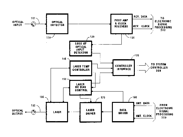
Turning now to Fig. 2 a description and explanation of
the operation of the FOU 100 of the above described system will
now be given. In the receive path, the Optical Fiber input 101 is
input to an Optical Detector 110. The Optical Detector converts
the optical energy into electrical signals and then amplifies the
received signals.
The amplified electrical signals are passed to a Post
Amp ~ Clock Recovery Circuit 120 where they are further amplified
and a clock signal is extracted from the input electrical signal.
The extracted clock is reclocked and the data and clock are passed
on to the ESP 200 via the RCV. DATA line and RCV. CLOCK line
respectively.
A Loss of Optical Input Detector 130 is connected to
the Post Amp ~ Cloc`k Recovery Circuit. The Loss of Optical input
Detector 130 is arranged to send an alarm signal to a Controller
Interface 190 whenever the optical input level drops below a
preset threshold. The Controller Interface 190 then outputs the
alarm to the SC 300.
In the transmit path, electrical signals in the form of
digital pulses and a clock signal are input to the Data Driver 180
from the ESP 200 on lines XMT. DATA and XMT. CLOCK respectively.
The Data Driver reclocks the data transmitted from ESP 200 using
the XMT. CLOCK signal. The output of the Data Driver 180 is sent
to the Laser Driver circuit 170 which in turn modulates Laser 160
converting the input electrical signals to an optical signal. The
Laser~s light output is coupled into a single mode fiber and
transmitted out on Optical Output 102.
The Transmit path further includes a Laser DC Bias
Control arranged to turn off the Laser 160 in case the data drive
fails. This prevents the Laser from being continuously turned on.
7~34
A Laser Temperature Controller 140 is also included and
used to control the lasers temperature and also the optical output
level. Both the Laser temperature controller 140 and Laser DC
Bias Control 150 send alarm signals to the Controller Inter~ace
190 in the event that the laser has failed~ its temperature is out
of limits, or the Data Drive circuit has failed.
Turning now to Fig. 3 a description of the loss of
optical input detector 130 of the present invention will be
explained in detail. When the optical input level detected by
optical detector 110 falls below a preset threshold indicating
either a loss of input or an unreliable input signal an AGC
control voltage generated within post amp & recovery circuit 120
goes high. This loss signal is input to the loss of optical input
detector via lead 10 to the base of transistor 12.
Transistor 12 is configured as a voltage follower,
which applies the loss signal via variable resistor 13 and fixed
resistor 15 to the base of transistor 20. Resistor 13 adjusts the
level of signal applied to transistor 20.
The differential pair shown as transistors 20 and 25
act as a voltage comparator. Transistor 25 receives a biasing
voltage from the voltage divider network comprising transistor 31
and resistors 30 and 32. The voltage applied to transistor 25
sets up a reference voltage which keeps the alarm network off.
When the input voltage to the differential pair exceeds
the reference voltage, that is, when the loss signal is applied to
the base of transistor 20, the voltage at the collector of
transistor 25 goes high. The high voltage at the colIector of
transistor 25 is coupled via resistor 33 to the base of transistor
40. This subsequently turns on transistor 40, causing light
emitting diode (LED) 42 to turn on and a negative logic signal to
be output via lead 44. The logic signal alarm is sent to the
controller interface 190 which signals the system controller that
a loss of optical input has occurred.
, . . .
~,
g ~37~04
~\
Although the preferred embodiment of the invention has
been illustrated, and that form described in detail, it will be
readily apparent to those skilled ln the art that various
modifications may be made therein without departing from the
spirit of the invention or from the scope of the appended claims.
; 6
:
.
:, ,. '.. ' ,''`' ::
: ~, ' '.' : ,