Note: Descriptions are shown in the official language in which they were submitted.
MONO~ITHIC LATTICE SAW FILTER
Backqround o~ Th~ Invention
The present invention genQrally rslates to
- 15 bandpass fllter~ a~d in particular to an improved SAW
bandpass filter with very low ins~rtioA los~.
SAW devices have ~raditionally been used in
transver~al typ~ ~ilter~. The key elemen~ ln SAW filter
design is th~ inte~digi~al tran~ducer (IDT); it con~erts
the electrical signal to the acoustic waveform and
thereby determines the filter impedanc~ and frequency
respon a. In thQ conv~ntional ~ er arrangement the
power is divided by the launching transducer. Half is
usually sent toward an absorber and half propagates
toward~ the output. At the output transducer, some of
the signal (at most half) is delivered to the load, some
pas3e~ the transducer and i~ absorbsd, and 30me i~
r~le~t~d. In instance~ where tha si~nal ra~lected by
th~ output IDT reach~ the in~u~ IDT part o~ it is
re~lected back to th~ output. Th~ doubly reflected
~ignal is detected at the output and cause~ passband
ripple.
-2 ~00144F
On~ solution ts this problem o~ having either
high insertion loss or significant ripple i9 ~0 use
unidirectional tran ducers to coupl~ all o~ the
electrical energy in~o a single acoustic wave.
Unidirectional transducers, however, ar~ mad~ wi~h phased
arrayR of electrode~, usually three or ~our ~lectrodes
per wavelength, which tends to complicate the ~abrication
proces~ by introducing ~ultiple layers o~ metalization.
Such an arrangs~ent may also limit filter bandwidth and
increas~ the component count.
SAW ~ilters in use today consist mainly o~ ~wo
ba~ic ~ype~: ~) Tran~versal ~ilter which includ~ a
~ending and a receiving transducer on a ingle ~ubstrate.
The selectivity characteristics are determined by th~
numb~r o~ ~inger pairs in ~he transducers and ~y the
~inger overlap g~ometry or "welghting". }n~ertion loss
~ends to b~ high b~cause simple transducers are
bidirectional i.e. one hal~ thQ input power i9
tran~mittsd in each o~ two opposit~ direG~ions. Various
method3 have been devi~ed to lower insertion loss such as
unidirectional transducers and multiple element
tran ducsr~ in parallel. However each o~ these ~ethods
ha~ ~evere d~ign rs~trictions and tend to be effective
only over a limited bandwidth and/or center frequency
range. ?) Coupled resonator filtQrs which include a
minimum of two acou~tically couplsd SAW resonators. They
ar~ ba~ically ~he equivalent o~ monolithic crystal
~llter~. The coupled bandwidth is controlled by ~he
indiv~dual re~onator geome~rie~ and t~Qir eparation.
Bandwidths ax~ limited to relatively narrow values and
d~sisn optimization will appear to require several
itera~ions.
-3- CM00144F
Summarv of The Invention
It is the ob~ect o~ thi~ invention to provide an
improved bandpa~s ~ilter which utilize~ SAW type devices
in a Pull la~tice circuit arranyement.
It is al~o an ob~ect o~ this in~en~ion to
provide a monolithic bandpas3 ~lltQr with all o~ the
dsvic2~ and interconnscts on a ~ingl~ substrate without
having electrical crossovers on the su~strate.
In accordanc~ with one aspect o~ this invention,
there is provided a bandpa~s filter that comprises a
~onolithic piezoelectric ~ubstrate and first and second
dual port SAW deYices di~posed on tha substrate and
coupled in a full lattlc~ c~rcuit con~lgura~ion. The
first lead of tho input of th~ filter is coupled to the
s~cond input~ of the f irst and second SAW d2vices and the
second lead o~ tho input of tha ~$1ter i~ coupled to the
first inputs o~ the fir~t and second SAW devices. Tha
Pir3t input oP ~he first SAW d~vic~ i5 coupled to the
seco~d output of ths c~cond SAW device to form the first
lead o~ ths filtar output. The ~ir~t output of the
second SAW d~vice i9 coupled ~o the second output o~ the
Pirst SA~ device to for~ the second filter output.
In accordance with another aspect o~ ~his
inv~ntion, there i~ provided a ban~pas~ fil~er comprising
a ~onolith~c pi~zoelsctric sub~tra~e and a f ir~t and
~econd ~et of elem~nts disposed on ~he substrate and
coupl~d in a cascad~d cir ui~ configuration. Each of the
set o~ element~ i~ com~rised of ~ir3t ~nd second dual
por~ SAW dovice electrically coupled to on~ another. The
fir~t ~et o~ elemen~ iY coupl~d to the input of ~he
f ilter and is coupled to the second s~t of elem~nts. The
second ~et o~ element~ i5 coupled to tha output of the
filter.
~8~
-4- CM00144F
Brief DescriPtiOn o~ The Drawinqs
Fig. 1 illustrates a latt~c~ circuit u~ing
element~ Za ~nd Zb.
Fig. 2 illu trat~s a dual port SAW transducer,
Fig. 3 illustrates a latti~e circult diagram
with two dual port SAW dQvics~ d~lqned according to the
~eachings o~ th~ presQn~ ln~ention.
Fig. 4 illustratss a ~our pol~ cascaded filter
utilizing dual port device~ according to the teachings of
this invention.
Flg. S illustrates the ~reguency re~pon~ for a
two pole lattic~ filter according to th~ teaching~ o~ the
present invention.
Detailed DescriPtion of The Preferr~d Embodiment
Fox a better understanding o~ the present
invention tog~thar with othsr and ~uxther a~vantages and
capabilitiQs thareof, re~erQnc~ i9 made to ~he following
dis lo~ure and appended claim~ in csnnection with the
abov~ described drawings.
SAW re~;orlators ars known to ~xhibit a certain
, l~v~l of re~onance ~h~t may be u~ful in cer~ain ~ilters.
How~v~r, les~ i known abou~ o~her SAW dsvice~ used in
f~lter~. With respact to SAW transdu er~, thQ equivalent
alectrical circuit of an unw2ighted ~AW tran~duc~r is, in
e~sence, the sam~ as that o~ a quartz cry~tal. A two
pola ~ilt~r may also be designed in a manner tha~ is
~i~ilar ~o a cry~tal ~ilter.
f,3~3~
-5- CM00144F
In the proposed filter, SAW devices are used as
individual resonators in a full lattice circuit. Fig, 1
represents a full lattice circuit having two Za elements
and two Zb elements. In a two pols filter, such a ~ull
lattice circuit arrange~ent would b~ rath~r inefficient
since four resonator~ would be required. However, due to
th~ fact that two identical Za and two identical Zb arms
axist in the circuit it is possible t9 use on~ resonator
in two ~laces. This could be accomplishsd by providing
~wo port~ ~or each resonator or dev~ce.
Referring to Fig. 2, ~h~r~ i~ illustrated a dual
port SAW ~ran~duce~ Or th~ typ~ that can be used as a
r~onator element in a lattice con~iguration, as in Fig.
3, or in a cascaded con~iguration, as in Fig. 4.
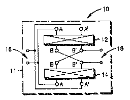
Raferrlng not to Fig. 3, thara ls illustrated a
bandpass ~ilter 10 that is di~poR~d on a 3ub~ra~e 11,
which i3 a ~onolithlc piezoelectric substrate. Filter 10
include~ two dual port SAW device~ 12 and 14 which are
dispo~ed on substratQ 11 and are couplQd in a full
lattice circuit configuration. The ~irst lead of input
16 o~ rilter 10 is coupled to kh~ second input3~
ds~ignated as A', o~ device 12 and device 14, The second
lead o~ input 16 of filter 10 is coupled to the first
input, des~gnated A, of devices 12 and 14. The first
; output of device 12, designated ~, i3 coupled to the
second output of davic~ 14, designated B', to form the
~rst lead of filter output 18. The ~irst output of
devic~ 14, d~signated 3, is coupled to th~ sscond output
o~ devic~ 12, which i~ designat~d B', to ~orm the second
lead o~ ~ilter output 18.
As illu~trated in Fig. 3, a lattic~
conriguration u~ilizing dual port SAW d~vices as elements
in thQ circuit reduceR tAe number of element~ required in
-6- CM00144F
a filter and reduces the overall sizD of ~he ~ilter. For
instance, a dual port device for device 12 sub~titutes
or ~he two Za elem~nt~ illustrated in Fig. 1. For a one
pole filter, device 12 would ~2 a two port SAW device and
device 14 would be comprised of two capacitors. In a two
pol~ ~ilter, devices 12 and 1~ would comprise dual port
SAW transducers or dual port SAW re~onatoxs. It is
possible to lncrsa e the number of poles ln this filter
by connec~ing a plur~lity o~ SAW devicss in parallel for
either device 12 or 14 or both. For example, a four pole
bandpa~s filter could be designed which is comprised of
two dual port SAW tran~ducer coupled in parallel for
davice 12 and two dual port SAW transducers coupled ln
parallel for devic~ 14. To hava filter 10 in~erface with
other component~, input 16 and output 18 may ~e coupled
to ex~rnal push-pull circuits or to an external
tr~n~ormer circuit.
In furtheranc~ o~ ~he teachings of the present
invention, ther~ i~ provided a monolithic SAW Xilter
d~vic2 with no el~ctrical crossovers on the substrate.
Thi~ feature o~ no electrical cro~sovers becomes
increaalng important at highQr freguencie~ and is
provided in a four pole ~ilter (illustra~ed in Fig. 4).
In Fig. 4 a bandpas~ filter 30 is ~llustra~ed which is
formed on a substrata 31, tha~ is comprised of a
monolithic piezoslectric substrate. Filter 30 i9 further
co~pri Qd o~ a fir~t and second sat of ele~ents disposed
~ on substrat~ 31 and coupled in a ca~caded circuit
configura~ion. ~arh o~ tha set o~ element~ is comprised
of two dual port SAW devices which ar2 electrically
csupled to one anothar. The first set of elements, which
i8 comprised o~ two dual SAW devices 32 and 34, is
coupled to ~he input 40 o~ filter 30 and is coupled to
th~ sQcond set og elements. The second set of alements,
which i~ comprised o~ two dual port SAW devices 3~ and
38, ar~ coupled to the output 42 of filter 30.
-7- CM00144F
Filteir 30 may include a plurality o~ se~s o~
dual port SAW devices dispos~id on substrate 31 and
coupled in a cascaded circui~ con~iguration if filter~
with a greater number o~ pole~ are required for higher
frequencies. For filters at le~s than a maximum
bandwidth, 90m8 capacitance, such ao capacitor 44, would
b~ reguired at the c nter junction. This could be
supplied by additional electrodas on the substrate. The
input and output termination~ o~ ~ilter 30 can not have a
common ground, ~here~ore coupling transformers would be
required for at least one port.
Refarring further to Fig. 4, ths output of
d~vicQ~ 32 and 34 ara coupled to one another and the
output~ o~ device~ 36 and 38 are also coupled to on2
another. The two ~et3 of eilements are electrically
coupled to each other by coupling one input o~ deivice 34
and one input o~ davica 38 ~o on~ another and coupling
th~ output3 of device~ 32, 34, 36 and 38 as illustrated
in Fig. 4. For a ~our pole filter th~ SAW devices in
Fig. 4 may comprisQ either dual por~ SAW ~ransducers or
dual port SAW re~onators. For higher order filter
de~gn~ the dual port SAW device~ may comprisc a
plurality of dual port S~W ~ran~duc~r~ couplsd in
parall~l-
; Th0 u~a o~ unweighted SA~ transducers doe~pres~nt some problem3. The reactancQ o~ ~h~i transducer
increa~es r~la~ively lineaxly with ~requency. However,
the Qquivalent re~istance cycle~ betwean zero and an
upper limit a~ a function of frequency. This
characteris~i~ cau ~ ripple~ in the fil~er fr~quency
respons~. To illustra~e thi problem a zero (O)dB or
Butt~rworth design was ussd so all of the passband ripple
can be attributed to the transducer variation. By
shi~tlng the relative fr~quency of two transducQrs
slightly, ~t has been found that passband ripple can be
reduced. This rasponsa is
-8- CM00144F
~hown in Fig. 4 ~or a two pole lattice ~ilter uslng 500
ringer pair SAW tran~ducers~ In a filter u~ing 1000
finger pair transducers the passband ripple i~
substantially reduced. In a four pole cascaded lattic~
filter using 1000 ~inger pair tran~ducers on lithiu~
tantalum oxide (LiTaO3) the passband ripple was
reduced. In su~h a ~our pole filter design two identical
sections are cascaded and by slightly ~tag~ering the
frequencies o~ the two sections the passband ripple can
be minimized.
In one embodiment o~ the ln~ention, ~he
monolithic SAW ~ilter wa~ deslgned with the following
parameters: a two ~2) pole 3utt~rworth ~ilter having a
center frequency o~ about 100 MHz and a 3 dB bandwidth of
abou~ 2 ~Hz. ~ual port SAW ~ransducers, of ~ type
illuskrated in Fig. 2, were used ~hat were fabricated on
LiTaO3 substrates having a 36 rotated Y cut~ Five
hundred (500) fing~r pairs par transducer were used, with
each transducer having an aperatur~ o~ about ~40
micrometers. The synchroni~m ~requency of th~ Za
transduc~r (or dQvice 12) was about 98.98 MHz and the
synchronism ~requency o~ the Zb transducer (or device 14)
was about 100.28 ~Hz. The terminating re~istance was
about ten (10) ohm~. The transducer~ are charac~erized
by uslng ~h~ "crossed-~ield" model as proposed by Smith
et. al. in: Analysi~ of In~erdigital Surface Wave
Tra~sduc r5 by U8~ of an E~uivalent Cir~uit Model, IEEE
Trans. on Mlcrowav~ Theory ~ Techniques, Vol. MTT-17, No.
11, No~. 1969.
Thus, th~rQ has been shown and described an
improved monolithic SA~ bandpass filter with very low
insQrtion 105~. Wi~h such a deRign, multipleopole
~ilters can be built acros~ a wide bandwidth range. Such
a desi~n also minimize~ the number of alemsnts necessary
-9- CMOal44F
in a filter and provides for a monolithic devicQ with no
electrical cro~sovers on the substrate, a fea~uro ~dhich
can beoome increa~ing important at higher ~requencie3.
The ~impllcity and compactness o~ this particular design
5 i9 n~w to filters for cellular telephone3 and ~runked
radios,
While there have been ~hown and described what
are at present considered the preferred embodlment~ of
~h2 invention, it will be obviou~ to tho~e sXilled in the
art ~hat variou~ changes and modific~tisns may bo made
therein without departing ~rom ~h~ scope o~ the invention
as de~ined by tha appended claim~.