Note: Descriptions are shown in the official language in which they were submitted.
i;~8~50
OVERSAMPLING A/D CONVERTER COMPRISING AN ADDITIONAL CAPACITOR
SWITCHED IN SYNCHRONISM WITH SWITCHING OF ~ INPUT CAPACITOR
BACKGROUND OF THE INVENTION:
This invention relates to an oversampling analog-to-dig~tal
(A/D or A-to-D) converter for sampling an input analog signal
at an oversampling frequency into an output digital signal.
An oversampling analog-to-digital converter is ordinarily
manufactured by using a very large scale integration technology
and is promissing in digital communication. By an oversampling
analog-to-digital converter, an input analog signal of an input
signal frequency bandwidth is sampled into an output digital
signal at an oversampling frequency which is much higher than
the input signal frequency bandwidth, for example, higher than
one hundred times the input signal frequency bandwidth.
An oversampling analog-to-digital converter is disclosed
in a report contributed jointly by Akira Yukawa, Rikio Maruta,
Yuulchi Kawakami, an~ Kyuichi Hareyama as Report No. 563 in Japanese
and with a title in English to "Sy8wa 59-nendo Densi Tîsin Gakkai
T~sin Bumon Zenkoku Taikai ~onbunsy~" (Reports for 1984 General
Meeting of Communication Branch of the Institute of Electronics
and Communication Englneers of Japan), under the title of "An
Oversampling A/D Converter Circuit Configuration for Digital
Codec IC." A similar and other oversampling analog-to-digital
converters are discussed in a paper contributed jointly by Akira
Yukawa, Rikio Maruta, and Kenji Nakayama to Proceedings of I~
International Conference on Acoustics, Speech, and Signal Processing
~1
5~)
held March 1985, pages 1400 to 1403, under the title of "An Oversam-
pling A-to-D ~onverter Structure for VLSI Digital CODEC's."
According to the Yukawa et al report and the Yukawa
et al paper, an oversampling analog-to-digital converter has
a converter input terminal supplied with an input analog signal,
An input switched capacitor is connected to the input terminal
and is for sampling the analog signal into output electric charges.
An integrator is for integrating input electric charges into
an integrated signal, which is quantized by a quantizer into
an output digital signal, A control logic is used in producing
a predetermined number of control signals in response to the
digital signal. A capacitor array is connected to a reference
voltage source and controlled by the control signals to produce
controlled electric charges. A connection is used in combining
the input switched capacitor and the capacitor array to the integrator
to combine the output electric charges and the controlled electric
charges into the input electric charges.
The oversampling analog-to-digital converter of the
Yukawa et al report 'or the Yukawa et al paper is excellently
operable to deal with the analog signal of an input signal dynamic
range which is approximately as wids as a power source voltage
used in putt~ng the converter into operation, It should, however,
be pointed out in the manner which will later be described more
in detail that the integrator is not operable at a high speed
in the converter of Yukawa et al, This lmposes an undesirable
restriction on the oversampling frequency, If the integrator
i8 somehow adapted to a high-speed operation, analog-to-digital
conversion becomes imprecise, Furthermore, the converter becomes
,.
,50
to require an unduly increased power consumption.
SUMMARY OF THE INV~NTION:
It is therefore an object of the present invention
to provide an oversampling analog-to-digital converter which
is operable at a high oversampling frequency,
It is another object of this invention to provide an
oversampling analog-to-digital converter of the type described,
which comprises an integrator operable at a high speed.
It is still another object of this invention to provide
an oversampling analog-to-digital converter of the type described,
by which analog-to-digital conversion can precisely be carried
out,
It is yet another object of this invention to provide
an oversampling analog-to-digital converter of the type described,
for which an undeslredly increased po~er consumption is unnecessary.
Other objeçts of this invention will become clear as
the description proceeds,
~ or describing the gist of this invention it is possible
to understand that an oversampling analog-to-digital converter
has a converter input terminal supplied with an input analog
signal and comprises an input switched capacitor connected to
the input terminal for sampling the analog signal into output
electric charges, an integrator for integrating input electric
charges into an integrated signal, a quantizer for quantizing
the integrated signal into an output digital signal, a control
logic responsi~e to the digital signal for producing a predetermined
number of control signals, a reference voltage source, a capacitor
array coupled to the reference voltage source and responsive to
so
the control signals for producing controlled electric charges,
and combining means connected to the input switched capacitor,
the capacitor array, and the integrator for combining the output
electric charges and the controlled electric charges into the
input electric charges.
According to this invention, the above-understood oversam-
pling analog-to-digital converter is characterized in that the
combining means comprises: (A) an additional switched capacitor
connected to the capacitor array for sampling in cooperation
with the capacitor array the controlled electric charges into
additional electric charges in synchronism with sampling of the
analog signal and (B) summing means connnected to the input switched
capacitor, the additional switched capacitor, and the integrator
for summing the output electric charges and the additional ~lectric
charges into the input electric charges
In the aboye-understood oversampling analog-to-digital
converter, the input switched capacitor comprises an input capacitor
connected to the converter input terminal, having a first capacitance,
and switched to produce the output electric charges, The integrator
comprises an operational amplifier having a positive input terminal
grounded, a negative input terminal, and an amplifier output
terminal for the integrated signal, The capacitor array com?rises
a common signal line, a reference capacitor having a reference
capacitance, and weighted capacitors having weighted capacitances
which are equal to 2k times the reference capacitance, respectively,
where k represents natural numbers starting at unity and ending
at the predetermined number less one. The reference capacitor
and the weighted capacitors are connected to the common signal
~8~25C)
line and coupled to the reference voltage source to be controlled
by the respective control signals and to collectively produce
the controlled electric charees.
In an example of the oversampling analog-to-digital
converter according to this invention, the integrator comprises
an integrating capacitor connected between the negative input
terminal and the output terminal and having a second capacitance,
The additional switched capacitor comprises an additional capacitor
connected to the common signal line, having a third capacitance,
and switched in synchronism with switching of the input capacitor
to produce the additional electric charges in cooperation with
the reference and the weighted capacitors. The summing means
is for connecting a combination of the input capacitor and the
additional capacitor to the negative lnput terminal. Under the
circumstances, each of the first through the third capacitances
is substantially equal to the reference capacitance-,
BRIEF DESCRIPTION OF THE DRAWING:
Fig, 1 is a block diagram of a conventional oversampling
analog-to-digital converter~
Fig, 2 is a block diagram of a basic oversampling analog-to-
digital converter;
Fig, 3 showst in blocks, an oversampling analog-to-digltal
converter according to an embodiment of the instant invention;
Fig, 4 is a block diagram of a control logic for use
in the oversampling analog-to-digital converter illustrated in
Fig,-~; and
Fig. 5, drawn below Fig, 2, is a block diagram of a
basic control loglc for use in describing the control logic sho~n
. .
9;~50
in Fig, 2
DES~XIPrION OF THE PREFE~RED EMBODIMENT:
Re~errin~ to Fig, 1, a conventional oversampling analog-to-
digital (A/D or A-to-D) converter will be described at first
in order to facilitate an understanding of the present invention.
The conventional oversampling analog-to-digital converter is
illustrated in Fig, 1 with a slight modification effected on
the oversampling analog-to-digital converter revealed in the
Yukawa et al report and the Yukawa et al paper, both referred
to hereinabo~e,
The oversampling analog-to-digital converter has converter
input and output terminals 11 and 12, The conYerter input terminal
11 is supplied with an input analog signal which hàs an input
signal frequency bandwidth t an input amplitude, and an input
dynamic range and should be ovsrsampled at an oversampling frequency,
The converter output terminal 12 is for an output digital signal
into which the analog signal is oversampled, Typically, the
input signal frequency bandwidth is 4 kHz wide, The oversampling
frequency is defined'by an oversampling clock sequence and is
much higher than the input signal frequency bandwidth, for example,
higher than one hur.dred times the input signal frequency bandwidth,
The oversampling clock sequence has alternatingly a binary zero
value and a binary one value in each oversampling period,
An input switch 13 is for connecting an input capacitor
14 alternatingly to the converter input terminal 11 and ground
when the oversampling clock sequence has the binary one and the
binary zero values, respectively, The input capacitor 14 has
a first capacitance Cl, A combination of the input switch 13
~,q,,
250
and the input capacitor 14 therefore serves as an input switched
capacitor which is connected to the input terminal 11 and is
for sampling the input analog signal at the oversampling frequency
to produce output electric charges dependent on the analog signal
and the first capacitance, It should be noted in connection
with the drawing figures that such switches are depicted as mechanical-
ly operable switches merely for convenience of illustration,
~ n~integrator 15 comprises an operational amplifier
16 having a positive or non-inverting input terminal grounded,
a negative or inverting input terminal, and an amplifier output
terminal. An integrating capacitor 17 has a second capacitance
~2 and is connected to the negative input terminal directly and
to the amplifier output terminal through a closing switch 1&.
An opening switch 19 is connected between the negative input
terminal and the amplifier output terminal, m e closing and
the opening switches 18 and 19 are operable in syr.chronism with
the input switch 1~ in the manner which will presently become
clear, The integrator 15 integrates input electric charges supplied
to the negative input terminal and produces an integrated signal
20 ; from the amplifier output terminal,
A quantizer 21 is for quantizing the integ~ated si~nal
into a quantized signal, Each bit of the quantized sign21 has
one of a preselected number of quantization levels, In the manner
known in the art, such a quantized signal ls unavoidably accompanied
by quantization noise, It is, however, possible to understand
insofar as an oversampling analog-to-digital converter is concerned
that the quantized signal is not much different from the output
digital signal.
~' .
89~50
In the example being illustrated, the quantizer 21
is implemented by a comparator whlch has a flrst comparison input
terminal supplied ~ith the integrated signal and a second comparison
input terminal grounded. m e quantizer 21 therefore produces
the quantized si~nal with each bit made to have one of a positive
and a negative level in each oversampling period as one of two
quanti~ation levels. In other words, the quantized signal represents
positive and negative signs.
Responsive to the output digital signal, a control
logic 22 produces a predetermined number of control signals.
When the predetermined number is denoted by a capital letter
K, the control signals can be identified as first through K-th
control signals, It will become clear later in the following
that each of such control signals has one of the binary one and
zero values in each oversampling period depending on a plurality
of digital signal bits which are equal in number to 2K and precedes
the oversampling period under consideration as preceding bits
in the digital signal. In the illustrated example, the predetermined
number is equal to f~ive,
A reference voltage source 23 is depicted to produce
a positive reference voltage (I Vr) and a negative reference
voltage (- Vr). A capacitor array 24 comprises a common signal
line, a reference capacitor having a reference capacitance C,
and a plurallty of weighted capacitorst (K - 1) in number, The
reference capacitor will alternatively be called a first capacitor,
Under the circumstances, the weighted capacitors are a second
through a K-th capacitor and have weighted capacitances which
are equal to 2, 22, 23, ..,, and 2K 1 times the reference capacitance,
~,'
; ' .
250
respectively. That is, the weighted capacitances are equal to
2 times the reference capacitance where the minuscule k represents
natural numbers starting at unity and ending at the predetermined
number less one, In the case under-~consideration where the predeter-
mined number is equal to five, the weighted capacitances areequal to 2C, 4C, 8C, and 16C,
A binary number of a plurality of binary bits, K in
number, is represented by the first through the K-th control
signals. The binary number is equal to a variable decimal number
L which is given by:
K (b 2k-l
k-l k (1)
where the coeffi`cients bk in the summation represent unity and
zero depsnding on the above-mentioned preceding bits of the output
digital signal, The variable decimal number becomes to have
a minimum value of zero and a maximum value of (2K 1 _ 1) only
when each coefficient specifically reperesents zero and unity,
respectively, Otherwise, the variable declmal number is between
the minimum and the maximum values, both exclusive,
In the capacitor array 24, the reference capacitor
and the weighted capacitors have their one ends connected to
the common signal line, Other ends of the reference and the
weighted capacitors are connected to the reference voltage source
- 23 individually through first through K-th switches which are
25 controlled by the first through the K-th control signals, respective-
ly, In this manner, each of the first through the K-th switches
correspond to one of the first through the K-th capacitors and
to one of the first through the K-th control signals, Through
250
each of the first through the K-th switches, a corresponding
one of the first through the K-th capacitors is supplied with
the positive reference ~oltage when a corresponding one of the
first through the K-th control signals has the binary zero value.
The corresponding one of the capacitors is supplied with the
negative reference voltage when the corresponding control signal
has the binary one value, In this manner, a combination of the
first through the K-th switches serves as a switch array 25 for
controllably connecting the capacitor array 24 to the reference
voltage source 23,
Controlled by the respectiYe control signals, the reference
capactior and the weighted capacitors collectively produce controlled
electric charges Qc which depend on the above-mentioned variable
decimal number L and are e~ual to 2Vr C L, The controlled electric
charges reach a maximum when the variable decimal number has .
the maximum value, namely, when each coefficient represents unity
in Equation (1),
It is now ~nderstood that the capacitor array 24 is
coupled to the reference voltage source 23 and is controlled
by the control : signals to produce the controlled electric
charges. More particularly, the re~erence and the weighted capacitors
are connected directly to the common signal line and coupled
to the control logic 22 through the switch array 25 to be controlled
by the respective control signals and to collectively produce
25, the controlled electric charges,
Turning to Fig. 2 during a short ~hile, a basic oversampling
analog-to-digital converter has converter input and output terminals
and comprises an integrator and a ~uantizer which correspond to
. .
11
similar parts described in conjunction with Fig, 1 and are designated
b~ like reference numerals 11, 12, 15, and 21. ~upplied with
the quantized signal from the quantizer 21, a digital-to-analog
(D/A) converter 2~ produces a local analog signal. An adder
27 is for subtracting the local analog signal from the input
analog signal to produce a difference analog signal, Responsive
to the difference analog signal, the integrator 15 delivers the
integrated signal to the quantizer 21,
A feedback loop is formed in this manner by the adder
27, the integrator 15, the quantizer 21, and the digital-to-analog
converter 26, A combination of the digital-to-analog converter
26 and the adder 27 is implemented in Fig, 1 by the input switched
capacitor, the control logic 22, the capacitor array 24 controlled
by the control signals, and the closing and the opening switches
18 and 19, The feedbàck loop is therefore put in operation at
the oversampling frequency, In this event, the quantiza~ior.
noise is localized to a high frequency band of the quantized
signal, A digital filter 28 is used to remove the quantization
noise from the quantized signal to deliver the output digital
signal to the converter output terminal 12 with high precision.
Inasmuch as the quantization noise is localized to the high frequency
band, the quantized signal is substantially identical with the
digital signal,
Turning back to Fig, 1, each of the first capacitance
Cl of the input capacitor 1~ and the second capacitance C2 of
the integrating capacitor 17 is equal to thirty-two times the
reference capacity C~ namely, equal to 32C, At each sampling
instant when the input capacitor 14 is connected to the converter
3\25C)
12
input terminal 11 through the input switch 13 while the opening
switch 19 is kept closed, the input capacitor 14 has electric
charges which are equal to 32C~Vi where Vi represents an instantaneous
voltage which the input analog signal has at the sampling instant
under consideration.
Outwardly of the capacitor array 24, the common signal
line is extended to the input capacitor 14 and to a point of
connection between the integrating capacitor 17 and the negative
input terminal of the operational amplifier 16. When the input
capacitor 14 is grounded through the input switch 13 concurrently
with closure of the closing switch 18, the electric charges of
the input capacitor 14 are moved to the integrating capacitor
17 as the output electric charges through the common sigpal line.
At the same time, the controlled electric charges are moved from
the common signal line to the integrating capacitor 17. It is
therefore ur.derstood in connection with the example being illustrated
that the common signal line of the capacitor array 24 serves
as a combining arrangement connected to the input switched capacitor,
the capacitor array 24, and the integrator 15 for combining the
output electric charges and the controlled electric charges into
the input electric charges,
As a consequence, the integrating capacitor 17 is given
moved electric charges Qm ~hich result from the controlled electric
charges and the output electric charges and are equal to (2Vr~C~L
- 32C-Vi), The integrator 15 produces the integrated signal
with an integrated voltage Vo which corresponds to a difference
calculated by the adder 27 described in conjunction with Fig.
2 between the ~oltage Vi of the input analog signal and a voltage
~;
... . , ~ ` .
' ,
of the local analog signal produced by the digital-to-analog
converter 26 depicted in Fig. 2. The integrated voltage Yo is
given by:
Vo - Qm/(32C) = 2Vr~L/32 - Vi (2)
It should be noted in ~ig, 1 that the integrator 15
is operable at a speed which is limited by the second capacitance
C2 of the integrating capacitor 17, To be more specific, the
integrating capacitor 1~ is nonnected to the amplifier output
terminal of the operational amplifier 16. The second capacitance
is as large as 32C. The operational amplifier 16 inevitably
has an output resistance R, The speed of operation of the integrator
15 is subjected to a limitation by a time constant which is equal
to 32C,R, As a consequence, the integrator 15 can not be operable
at a hlgh speed. This imposes an undesirable restriction on
the oversampling frequency.
It is seemingly possible to raise the speed of ~o~è~ation
of the integrator 15 by reduclng the second capacitance C2,
It is, however, difficult in practice to make a capacitor have
a small capacitance accurately, It becomes impossible to make
the oversampling analog-to-digital converter precisely carry
out the analog-to-digital conversion.
The speed of operation of the integrator 15 can alternative-
ly be raised by reducing the output resistance of the operational
amplifier 16. It is in fact possible to reduce the output resistance.
This, however, results in an intricate output circuit and accordingly
in an unduly lncreased power consumption,
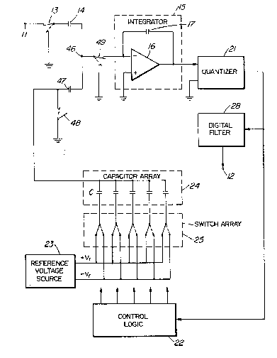
Referring now to Fig, 3, the description will proceed
to an oversampling analog-to-digital converter according to a
~''';`P'
:~
" ' ~''' ' ,
- '
'': ' ., . , `
~ .
250
preferred embodiment of this invention. The converter has converter
input and output terminals and comprises similar parts which
are designated by like reference numerals 11 through 17, 21 through
25, and 28.
It should be noted as regar~s this converter that the
first capacitance Cl of the input capacitor 14 and the second
capacitance C2 of the integrating capacitor 17 are rendered astonish-
ingly smaller than the first and the second capacitances described
in connection with Fig. 1. The first and the second capacitances
Cl and C2 will later be exemplified. Incidentally, a cantrolled
voltage is developed by the controlled electric charges Qc on
the common signal line of the capacitor array 24.
Turning temporarily to Fig. 4, the control logic 22
will be described a little more in detail, It will be presumed
that the predetermined number X is equal to five as before,
A delay circuit 31 gives a delay of one oversampling
period to the quantized signal which is supplied from the quantiæer
21 depicted in ~'igs. 1 through 3 and may be called the output
digit~l signal in thé manner pointed out above. The delay circuit
31 thereby produces a delayed digital signal, which is inverted
by an inverter 32 into an inverted digital signal. When the
input analog signal is higher than the controlled signal, the
integrated voltage Yo becomes negative acco-ding to Equation
(2), In this event, the inverted signal has a positive level,
When the analog signal is lower than the controlled signal, the
inverted signal has a negative level,
In the manner known in the art, a polarity counter
33 is supplied with the inverted signal to produce a count signal
'_
.
:
A and a polarity signal B. The count signal A is used in counting
up ~nd down an up-down count in an up-down counter 34. Inasmuch
as the predetermined number K is equal to five, the up-down counter
34 has first through fifth stages 2 to 2 to supply a digital
adder 35 with first through ~i`fth binary signals collectively
representative of the up-down count. When the up-down count
reaches 00000 and should be further counted down, the up-down
counter 34 delivers a switching signal C (designated by the reference
lette~ for the reference capacitance merely for convenience)
to the polarity counter 33.
It will be assumed that the converter input terminal
11 (Figs, 1 to 3) is supplied with the input analog signal which
is positive and increasing. In the mean~hile, the polarity signal
~ has the binary zero value. When the inverted signal has the
positive level, the count signal A has the binary one value to
count up the up-down count in the up-down counter 34. ~hen the
inverted signal has the negative level, the count signal A has
the binary zero value to count down the up-down count.
It will be'assumed that the input analog signal is
negative and has an increasing amplitude. In this event, the
polarity signal 3 has the binary one value. ~hen the inverted
signal has the positive level, the count signal A has the binary
zero value to count down the up-down count. When the inverted
signal has the negative level, the count signal A has the binary
one value to count up the up-down count.
` As a result, the first through the fifth binary signals
are produced by the up-down counter 34 so that the up-down count
follows a change in the input analog signal, Adding as a summand
16
- the binary one or zero value of the count signal A supplied from
the polarity counter 33, the digital adder 35 produces first
through fifth digital signals Dl to D5.
A clock input terminal 36 is supplied with the oversampling
clock sequence, It should be noted that the oversampling clock
sequence is delivered through connections (not depicted merely
for simplicity of illustration) to the input switch 13 (Eig, 3)
and to two other switches which will shortly be described,
In the example being illustrated, a sampling gate circuit
37 consisits of first through fifth AND gates supplied with the
first through the fifth digital signals Dl to D5, respectively,
and with the oversampling clock sequence in common, A polarity
gate circuit 38 consists of first through fifth Exclusive OR
gates which are coupled to the first through the fifth AND gates,
respectively, and are supplied with the polarity signal B in
common. At each sampling instant where the oYersampling clock
sequence has the binary one value, the first through the fifth
digital signals Dl to D5 are delivered through the sampling gate
circuit 37 to the poiarity gate circuit 38 as they are, At each
lntegrating instant where the oversampling clock sequence has
the binary ~ero value, the sa,~pling gate circuit 37 delivers
the binary zero value to the polarity gate circuit 38,
In the polarity gate circuit 38, the first through
the fifth Excluslve OR gates produce first through fi`fth unit
signals El to E5, respectively. It will be surmised that the
polarity signal B has the binary zero value, In this case, the
unit signals El through E5 have the binary one and/or zero values
which are identical in each sampling instant with those had by
?~
- .
39~5~)
digital signals Dl through D5, respectively, The unlt signals
El through E5 simultaneously have the binary zero value in each
integrating instant. When the polarity signal B has the binary
one value, the unit signals El through E5 are inverses of the
respective digital signals Dl to V5 in each sampling instant.
The unit signals El through B5 concurrently have the binary one
value in each integrating instant,
Further turning to Fig, 5, a basic co~trol logic will
be described for a better understanding of the control logic
22 illustrated with reference to Fig, 4, Fig, 5 is a reproduction
of one of eight figures which are shown in the Yukawa et al paper
referenced heretobefore,
The basic control logic comprises a first delay circuit
and an inverter which correspond-to the delay circuit 31 and
the inverter 32 described in conjunction with Fig, 4 and are
therefore designated by the reference numerals 31 and 32, The
inverted signal is delivered to an input adder 41 which produces
a first sum signal in the manner which will very soon beco~e
clear, A second delay circuit 42 gives a delay of one oversampling
period to the first sum signal to produce a delayed sum signal,
which is delivered to the input adder 41 to result in the first
sum signal, L~ output adder 43 produces a second sum signal
representative of a sum of the inverted sigr.al and the first
sum signal,
It will be understood that a combination of the input
; adder 41 and the second delay circuit 42 serves as a digitalintegrator for integrating the inverted signal and is implemented
in Fig. 4 by the up-down counter 34, The output adder 43 corresponds
.~ . . ~ `
.
~8~SO
18
in Fig. 4 to the digital adder 35.
Referring back to Fig. 3, the first through the fifth
control signals are the first through the fifth unit signals
El to E5 described in connection with Fig. 4. In the switch
array 25, a first switch supplies the reference capacitor of
the reference capacitance C with the negative reference voltage
(- Vr) and the positive reference voltage (~ Vr) when the first
control signal has the binary zero and the binary one values,
respectively. In this manner, the capacitor array 24 produces
the controlled signal described above,
It may be mentioned here that the predetermined number
K is determined as follows, In the manner taught in the Yukawa
et al report referred to hereinabove, the oversamplingyfrequency
is given by:
Fc = 27l~foA/S,
whe~e Fc represents the oversampling frequency, f represents
the input signal frequency bandwidth, A (designated by the reference
letter for the count signal merely for convenience) represents
a half of the afore-described input signal dynamic range, and
; S represents a unit step voltage of the controlled signal, namely,
is equal to the absolute value of the positive and the negative
reference Yoltage over the maximum value of the variable decimal
number L described before. In consideration of the input signal
dynamic range, the predetermined number K is determined in compliance
with~
K ~ log2(2A/S) - log2(Fc/[ ~'f~)
If 1,024 kHz is used as the oversampling frequency for an input
analog signal having an input signal frequency bandwidth of 4
so
19
kHz, the predetermined number K should be 6.3 or greater, namely,
should preferably be equal to seven,
Referring more particularly to Fig, 3, the input capacitor
14 has an input end connected to the input switch 13 and an output
end led to a point 46. An additional capacitor 47 is interposed
between the point 46 and the common signal line of the capacitor
array 24 and has a third capacitance C3 which is of the order
of the first or the second capacitance Cl or C2. More specifically,
the additional capacitor 47 has a first end connected to the
common signal line and a second end connected to the point 46.
An additional switch 48 is for disconnecting and connecting the
common signal line to ground and consequently the first end of
the additional capacitor 47 to ground.
The integrator 15 comprises only the operational amplifier
16 and the integratlng capacitor 17 and does not comprise the
clo$ing and the opening switchis 18 and 19 (Fig. 1). Instead,
a connecting switch 49 connects the point 46 of connection between
the input and the additional capacitors 14 and 47 to the negative
input terminal of the operational amplifier 16 and to ground.
Speaking of the switches 13, 48, and 49 more in detail,
the input switch 13 connects the input capacitor 14 to the converter
input terminal 11 ~nd to ground when the oversampling clock sequence
has the binary one and the binary zero Yalues in each oversampling
period, respectively, The àdditional switch 48 disconnects and
connects the common signal line and hence the first end of the
additional capacitor 47 to ground when the input switch 13 connects
the input capacitor 14 to the converter input terminal 11 and
to ground, respectively, The connecting switch 49 connects the
~''"
'
point 46 of connection to the negative input terminal and to
ground when the input switch 13 connects the input capacitor
14 to the converter input terminal 11 and to ground, respectively.
When concurrently grounded through the input switch
13, the additional switch ~8, and the connecting switch 49, the
input capacitor 14, the additional capacitor 47, and the reference
capacitor and the weighted capacitors of the capacitor array
24 have no electric charges, At each sampling instant when the
oversampling clock sequence has the binary one value, the input
capacitor 14 is switched by the input switch 13 to the converter
input terminal 11 to sample the input analog signal into the
output electric charges in the manner described before. ~eing
simultaneously disconnected from ground, the additional capacitor
47 is supplied from the capacitor array 24 with the above-mentioned
controlled electric charaes Qc which is equal to 2Vr C-L. The
additional capacitor 4~ therefore produces additional electric
charges in cooperation ~ith the reference and the weighed capacitors,
equal in number to the predetermined number K less one. The
reference voltages (~ Vr) and (- Yr) need not be different from
those used in the conventional oversampling analog-to-digital
cor.verter illustrated with reference to Fig, 1,
At this instant, the connecting switch 49 is discor~ected
from ground to deliver the output electric charges and the additional
electric charges to the integrator 15 as the afore-mentioned
input electric charges. When calculated by using the conservation
law of electric charge, the integrated voltage Vo becomes:
Vo = (C3/C2)~2VrCL/(31C + C3) - (Cl/C2)-Vi (3)
which equation is identical with Equation (2) when each of the
~r~
.
21
~irst through the third capacitances Cl to C3 is equal to the
reference capacitance C.
Each of the first through the third capacitancec Cl
to C3 need not be equal to the reference capacitance C. In this
event, Equation (3) is not identical with Equation (2). It is,
however, obvious; that the oversampling analog-to-digital converter
is operable like the conventional one and that each of the first
through the third capacitances Cl to C3 should preferably be
either substantially equal to the reference capacitance C or
be of the order of the reference capacitance C,
Reviewing Fig, 3 in consideration of the foregoing,
it is mderstood that a combination of the additional capacitor
47 and the additional switch 48 serves as an additinoal switched
capacitor connected to the capacitor array 24 to sample the controlled
electric charges into the additional electric charges in synchronism
with.sampling of the input analog signal by the input switched
: capacitor and ir. cooperation with the capacitor array 24 having
a total capacitance which is equal to a sum of the reference
capacitance C and the weighted capacitances, equal in number
to the predetermined number K less one, m e total capacitance
is equal to 31C when the preaetermined number is equal to Iive,
The afore-mentioned combining arrangement comprises the sdditional
switched capacltor and a summing circuit which is connected to
the input switched oapacitor, the addltinoal switched-c~apacitor
and the integrator 15 to sum the output electric charges and
the àdditional electric charges into the input electric charges,
More in detail, the additional switched capacitor comprises
the additional capacitor 47 switched in synchronism with switching
!,
,
~'
' ' ' ' ' '' " ' ' ' ' ~
.
''''
~.~8~1250
22
of the input capacitor 14 to produce the additional electric
charges in cooperation with the reference capacitor and the weighted
capacitors, equal in number to the predetermined number less
one, The summing circuit comprises the connecting switch 49
for connecting a combination of the input capacitor 14 and the
additional capacitor 47 to the negative input terminal of the
operational amplifier 16 in synchronism with switching of the
input:capacitor 14, As the case may be, the quantizer 21 should
be understood to include the digital filter 28 so as to deliver
the output digital signal directly to the converter output terminal
~2 ln response to the integrated signal,
Furthermore, it is appreciated that the integrator
15 is operable at a high speed insofar as the second capacitance
C2 i8 of the order of the reference capacitance C, ~ore particularly,
the above-mentioned time constant becomes equal to C2-R and is
unexpectedly smaller than the time constant which is equal to
32C,R in the conventional oversampling analog-to-digital converter,
This makes it uncesessary that the input capacitor 14, the integrating
capacitor 17, and the reference and the weighted capacitors of
the capacitor array 24 should have small capacitances which are
difficult to realize with precision, mis moreover makes it
unnecessary to use an intricate output circuit, As a resultt
the oversamplin~ analog--to-digital converter can produce the
output digital signal at a hlgh oversampling frequency, with
: :25 precision, and without an unduly increased power consumption,
:~
, ~ '
:
.:
:-