Note: Descriptions are shown in the official language in which they were submitted.
ISDN INTERFAC~ TRUNK CIRCUIT
CROSS REFERENCE TO RELATED APPLICATIONS
The present application is related to copending Canadian
patent applications serial numbers 565,366-5 and 365,364^9 which
have the same inventive entity and are assigned to the same assignee
as the present U.S. patent application.
BACKGROUND OF THE INVENTION
The present invention pertains to Integrated Services
for Digital Networks (ISDN) and more particularly to trunk circuitry
for interfacing between an ISDN system and T-carrier facilities.
In general, an Integrated Services Digital Network is a
system which provides end to end digital connectivity to a wide
variety of services by users having multi purpose user network
interfaces. ISDN systems provide voice switching, packet data
switching, signalling networking and wideband networking
capabilities.
ISDN systems typically provide for data transmission and
reception employing a particular format. Usually, this format is
incompatible with T-carrier data formats. The data transmission
rates of ISDN systems and T-carrier facilities are typically in the
megabit per second range. Conversion of data from the ISDN format
to the T-carrier format and vice versa must be done rapidly. In
addition, circuitry must operate both for receiving and transmitting
data simultaneously.
25 / Further, due to the flexibilities of the ISDN system,
large strings of logic O data is produced. In contrast, T-carrier
facilities cannot tolerate more than 15 consecutive logic zeroes in
a string of transmitted data bits. Therefore, interfaces between T-
carrier facilities and ISDN systems require high-speed conversion of
strings of zero data into non-zero data strings and high-speed
recovery of the zero data strings at the distant end of the T-
carrier facility.
Therefore, it is an ob~ect of the present invention to
provide a high-speed receiver/transmitter interface between T-
carrier facilities and an ISDN system.
1~39~5Z
It is another obiect of the present invention to
provide a high-speed zero data bit conversion and recov~ry
arrangement.
SUMMARY OF THE INVENTION
In accomplishing the objects of the present invention,
there is provided a novel interface trunk circuit connected
between T-carrier facilities and an ISDN system.
The interface trunk circuit is used for receiving and
transmitting data between T-carrier facilities and ISDN systems.
The interface trunk circuit is connected between the T-carrier
facilities and the ISDN systems. The interface trunk circuit
includes a first receiver which is connected to the ISDN system.
The first receiver operates in response to a first serial input
data stream, a clock signal and a framing signal to produce a
first parallel data stream. A memory is connected to the first
receiver and operates to store the first parallel data stream.
A processor is connected to the memory. The processor
operates in response to the first parallel data stream to convert
predetermined lengths of logic zeroes in this data stream to logic
non-zero data streams of the same length.
A first transmitter is connected to the memory. The
first transmitter operates in response to the previously stored
logic non-zero data stream to convert this data stream to a first
serial output tata stream and to transmit this converted data
stream via the T-carrier facilities.
A secont receiver is connected to the T-carrier
facilities. The second receiver operates in response to a second
serial input data stream from the T-carrier facilities to convert
the received second serial input data stream to a second parallel
input data ~tream. The memory is connected to the second
receiver. The memory is operated in response to a timing signal
to store the second parallel data stream simultaneously with the
storage of the first parallel data stream and simultaneously with
the transmission of the logic non-zero data stream. The processor
~; 35 al80 operates in response to the second parallel data stream to
~ -
~28925~
convert logic non-zero data streams to logic zero data streams for
storage in the memory.
A second transmitter is connected to the memory and to
the ISDN systems. The second transmitter operates to convert the
second parallel data stream, which contains logic zero data
streams, to a second serial output data stream. The second
transmitter then transmits this second serial output data stream
to the ISDN systems via a data output lead.
A BRIEF DESCRIPTION OF THE DRAWINGS
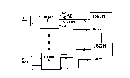
Figure 1 is a block diagram of the primary trunk
interface between T1 digital spans and an ISDN switching system.
Figure 2A is a frame layout of T1 data format.
Figure 2B is a frame layout of the extended framing
format.
Figure 3 is a frame format of data sent between the
ISDN copy and the trunk.
Figure 4 is a block diagram of the trunk shown in
Figure 1.
Figure S is a memory layout of the dual port random
access memory (RAM).
Figure 6 is a state machine circuit for controlling
access to RAN nemory.
Figure 7 is a memory address control circuit for RAN
memory.
DESCRIPTION OP THE PREFERRED EMBODIMENT
Figure 1 depicts the interconnection of the primary
trunk circuit between a digital Tl span and duplex copies of an
ISDN (Integrated Services Digital Network) system. ISDN copy 0 is
connected via four leads to each of the trunk circuits. Copy 1 of
the ISDN system is also connected via four similar leads to each
trunk. Trunk circuits are shown in this system, however, line
circuits for connecting the ISDN system to subscribers may be used
in addition to trunk circuits or in place of the trunk circuits.
The four leads connecting each ISDN copy to a trunk or
line include a clock signal CLK, a framing signal ESP, a serial
8~252
data in signal DIN and a serial data out signal DOUT. The CL~
signal is a 1~.352 MHz signal which is sent from the ISDN syste~
to the trunk. The 12.352 MHæ signal is divided by four (4) to
derive a 3.088 MHz signal for ISDN data. The 12.352 MHz signal
supplied by the ISDN system is also div~ded by eight (8) to
produce a 1.544 MHz signal for clocking data out via the T1 span.
ESP is a framing signal for the data transmitted from the ISDN
system to the trunk. The data DIN and data DOUT leads
respec~ively transmit data to and from the trunk circuit. ISDN
copy O and copy 1 are interconnected to provide for synchronous
redundant operation.
Each trunk circuit is also connected to a Tl span. The
T1 spans transmit data between the trunk and other distant trunks
or switching systems.
The framing format of the tata transmitted between the
trunk circuit and distant trunks or switching systems tnot shown)
via the Tl lines is shown in Figure 2A. This is a T1 line format
based upon a standard 1.544M bits per second DS1 digital
signalling format. The DS1 frame contains a 193 bits of
information. This informat~on is composed of a single
synchronization or framing bit plus 192 bits of data. The 192
bits of data are organized into 24 channels of 8 bits each. Each
8 bit quantity may be referred to as a channel or an octet.
Each channel or octet consists of 8 bits, PCMO - PCM7.
PCMO is a sign bit. PCM1 - PCN7 inticate the magnitude of the
voice sample. By a strapping option on the trunk printed wiring
card, the T1 data format shown in Figure 2 may be provided.
However, a preferred arrangement includes an "extended super
framing format" which includes a CRC bit and data along with the
framing bit distributed over a 24 frame sequence.
Twenty-four channels are organized together with an
S-bit to form a frame. Each sample in the frame is associated
with one channel of voice or data. The channels are numbered O
through 23. The S-bit carries a periodic pattern which, when
detected, is used to identified th. beginning of each frame of
`;
:
z~z
data. Twent~-four (24) frames of data are organi2ed to for~ a
superframe. This extended framing format is shown ~n Figure ~s.
The periodic pattern of data carried by the S-bit also makes it
possible to identify the individual frames within a superframe.
For the extended super framing format (ESF), the S-bits of frames
1, 5, 9, 13, 17 and 21 follow the bit pattern shown in Figure 2A.
These TS-bits and FS-bits provide for framing and frame number
identification.
In the ESF format, the S-bits of frames 3, 7, 11, 15,
19 and 23 provide the cyclic redundancy check (CRC) function. The
remaining S-bits provide a 4 KB/sec channel. At present 2 KB/sec
of this channel are used for Zero Byte Time Slot Interchange
(ZBTSI) encoding and flags.
Figure 3 depicts the format of data transmitted between
each ISDN copy and the trunk. One frame of data comprises 32
channels of information plus a F-bit and a U-bit. At present, the
F bit is unused. The U bit is used for the transmission of
information between the ISDN copy and a processor contained on ~he
trunk circuitry.
Each channel includes 12 bits of information. The
first 8 bits of each channel are the data bits ~similar to the
PCMO - PCM7 bits of the DSl format). The informa~ion contained in
these bits may be either data or voice information. ~ext, 3 bits
are designated as SIG or signalling bits. Last, a parity bit
follows the signalling bits. The parity bit carries odd parity
over the other ll-bits of each channel.
Data shown in the format of Figure 3 is transmitted
from the ISDN copy O to demultiplexer 12 shown in Figure 4. The
12 megahertz clock signal CLK and the framing signal ESPO are both
transmitted from ISDN copy O to timing and control circuit 10.
Timing and control circuit lO operates demultiplexer 12 to remove
~, the F and U bits from the tata stream. Since the F-bit is
presently unused, it is tiscarded. Demultiplexer 12 transmits the
U-bit to latch 14 where it is stored. Demultiplexer 12 then
transmits the serial PCMR bit stream to 2 to 1 multiplexer 16 and
to parity check circuit 22.
.. .. ` .
'~
9252
Parity check circuit 22 calculates the parity o~er each
channel, tha~ is, the 8 data bits and 3 signalling bits. The
parity check circuit 22 then compares the calculated parity with
the parity bit found in each channel to determine that each
channel has properly been received. If a miscomparison is
detected, ehe parity check circuit 22 generates an interrupt to
the microprocessor 100.
Two-to-one multiplexer 16 selects the serial PCMR data
input from either copy 0 or copy 1 to be transmitted to the dual
port RAM 20. Serial to parallel converter 18 converts the 8 data
bits of each channel from serial to parallel and stores these
8-bits in dual port RAM 20 via the right port. The right port of
RAM 20 is setup to alternately store bytes transmitted from
converter 18 first in an even numbered byte and then in the next
sequential odd numbered byte. This process is then repeated for
each channel transmitted from the ISDN copy. A memory layout of
the dual port RAM is shown in Figure 5.
Similarly, ISDN copy 1 transmits data via the DINl lead
to demultiplexer 32. Twelve megahertz clock CLRl and framing
signal ESPl are transmitted to timing and control circuit 30.
Demultiplexer 32 removes the F-bit and the U-bit. The F-bit is
discarded since it i9 unused. U-bit is transmitted from
demultiplexer 32 to laech 34 where it is stored.
The serial PCMR data received from ISDN copy I is
~5 transmitted from demultiplexer 32 to parity check circuit 42 and
to multiplexer 16. Parity check circuit 42 calculates the par~ty
over the 8 to data bit~ and 3 signalling bits of each channel and
compares it with the parity bit transmitted in each channel. If a
miscomparison iB detected, parity check circuit 42 interrupts
microprocessor 100 to set an alarm for this condition.
The signalling bits are removed from each channel of
data transmitted from copy 1 and stored in config latches 33. The
signalliDg bits from ISDN copy 0 are removed and stored in config
latches 13. Each of the config latches 13 and 33 transmits two of
the signalling bits to the copy select circuitry 15. Nith these
~:~8~25:!
bits the copy select circuitry deter~ines which copy of the data
transmitted from the ISDN system is to be output by the trunk on
the Tl span. The copy select circuit controls multiplexer 16 in
order to select the data stream from either copy 0 or copy 1 of
the ISDN system.
After data has been stored in the dual port RAM 20 for
transmission via the T1 span, digital signal processor 90 formats
the data for transmission on the Tl span. This data ~s formatted
according to the structure shown in Figure 2B. Because the T1
system is capable of providing a 64 KBS (clear channel)
transmission, the digital signal processor 90 performs a Zero Byte
Time Slot Interchange (ZBTSI) scheme. This scheme insures that no
more then 15 consecutive logic zeroes are transmitted on the Tl
span. There are many techniques for Zero Byte Time Slot
Interchange. The digital signal processor 90 may be programmed
for any such scheme.
Digital signal processor 90 accesses dual port RAM 20
via a 16 bit wide bus. The data is then read out of RAM 20 one
byte (8-bits) at a time. The data is transmitted from dual port
RAM 20 to parallel to serial converter 24. The serial bit stream
is then transmitted from converter 24 to frame generator and the
Cyclic Redundancy Check (CRC) generator 26. Frame generator and
CRC generator 26 adds the framing and CRC check bits to the data
stream and places the resultlng data on the Tl span for
transmission to a distant system.
Data received from a distant system via the T1 span is
transmitted to frame check, CRC check and received clock
generation circuit 28. Circuit 28 removes and checks the framing
and CRC bits with one which it has calculated. Circuit 28
generates an alarm if a miscomparison is detected. In addition,
circuit 28 also recovers the data received clock signal which is
1.544 MB per second. The serial data is then transmitted from
circuit 28 to serial to parallel converter 50. Converter 50
converts the data into 8-bit bytes and stores each byte in aua
port RAM 20. Four frames of data must collected before it is
:`
' '
.
.
'
~f~
deter~ined whether a Zero ~yte Time Slot Interchange scheme has
altered any data bytes. If data bytes have been altered, the
digital signal processor 90 reads and recovers the origlnal data
transmitted by the distant office. The recovered data is stored
in memory 20.
~ hen all the data has been recovered, the data is then
transmltted 8-bits at a time from RAM 20 through parallel to
serial converter 52. Parity generator circuit 54 generates the
parity for each byte of information and inserts the parity bit
into the serial bit stream PCMX. This serial bit stream is then
transmitted to ~ultiplexers 56 and 66. Ti~ing and control circuit
10 enables multiplexer 56 to transmit the data via the DOUTO lead
to ISDN copy 0. Timing and control circuit 30 enables multiplexer
66 to transmit the serial PCMX data via the DOUTl lead to ISDN
copy 1. Each of the ISDN copies receive the same data, since one
is the redundant backup unit for the other.
A Rockwell integrated circuit part number 8070 may be
employed to achieve such functions in the circuitry shown as
serial to parallel conversion, parallel to serial conversion,
framing generation and checking and CRC generation and checking.
Microprocessor 100 may be implemented with a microprocessor
integrated circuit part number 8744. Digital signal processor 90
may be implemented with a Texas Instruments integrated circuit
part number 32020. The digital signal processor 90 is a 16-bit
wide processor which has an approximate instruction cycle time of
100 nanoseconds.
Referring to Pigure 6, the circuitry for controlling
data transfer between the dual port RAM 20, the T1 span and the
ISDN system is shown. For this portion of the explanation, it
wlll be assumed that one byte of data has been transferred through
multiplexer 16 from an ISDN switch into serial to parallel
circuitry 18, as shown in Figure 4.
Tha serial to parallel circuitry 18, as shown in Figure
6, comprises serial to parallel shift register 130; data latch
132, which is connected between the data bus and serial to
~,
z
parallel shift register 130; address counter 134 and address latch
136, which is connected between address counter 134 and the
address bus. Latches 132 and 136 and register 130 are each 8-bits
wide.
Since serial data has been transmitted to reg~ster 130
from the ISDN syste~, a byte of information has been collected in
register 130. At this point, the ATIME signal ~s generated by
ti~ing and control circuit 10 or 30. This causes the transfer of
data from register 130 to latch 132 and the transfer of the
corresponding address from address counter 134 to address latch
136. The ATIME signal also sets flip-flop 112 which in turn
generates the RQSTA signal. In addition, the ATIME signal clocks
latches 132 and 136. The generation of the RQSTA signal causes
programmable read only memory (PROM) 101 to be read at the address
indicated by the value of the RQSTA-RQSTD signals. As a result,
the binary value 0001 is output to PROM 101 via the four output
leads which connect PROM 101 to binary counter 105. Also, PRON
101 generates a load signal which causes binary counter 105 to be
enabled via OR gate 103 and the ENB1 lead.
At the next cycle of the clock (not shown), the CLK
signal causes binary counter 105 to be loaded with the four
outputs of PROM 101. Binary counter 105 begins counting a
sequence from the initial value input from PROM 101. This value
is 1, so the counter begins counting from binary 1. In sequence,
binary counter 105 produces signals on each of the leads SQ1, SQ2,
SQ3 and SQ4 in response to further successive clock signals.
Each of the generated signals, SQ1 through SQ3, are
transmitted from decoder 110 to OR gate 138 via the corresponding
,leads. For the duration of each of the signals SQ1 through SQ3,
OR gate 138 enables data latch 132 to place the stored data byte
on the data bus for transmission to RAM 20. OR gate 138 also
enables address latch 136 to place the stored address onto the
address bus for transmission to RAN 20.
Given the data byte and address from latch 132 and
latch 136 respectively, RAM 20 stores the data byte at the
''' ' ' :
:''.
'12~9~S~
indicated address. This occurs during the SQ2 signal, which
enables OR gate 118 to produce the wTite (WR) signal. The SQ2
signal is also transmitted to flip-flop 112 and causes flip-flop
112 to reset the RQSTA signal.
Prior to the time the SQ4 signal is produced, the data
write operation to RAM 20 is complete. When the signal SQ4 is
produced by decoder 110, OR gate 107 is enabled and binary counter
105 is reset and stops counting. This terminates the data
transfer operation for the particular byte of data which is
received from the ISDN system.
Serial to parallel circuit 50 of Figure 4 is shown in
Figure 6 in detail. Similar to circuit 18, circuit 50 includes a
serial to parallel shift register 150; data latch 152, whlch is
connected between the data bus and register 150; address counter
154; and address latch 156, which is connected between the address
bus and address counter 154.
Similar to operation of circuit 18 above, when data is
transmitted from the T1 span, a byte of information is collected
by serial to parallel shift register 150. At the same time, the
framing circuitry 28 generates the RQSTB signal. The RQSTB signal
is also input to latches 152 and 156. This signal produces the
binary value 0010 which is input to PROM 101. As a result, the
PROM 101 outputs the binary value 0101 to counter 105. Counter
105 begins counting at 5.
In response, decoder 110 produces signals SQ5, SQ6,
etc. on each successive clock cycle. Signals SQ5, SQ6 and SQ7 are
transmitted from decoder 110 to OR gate 158 via the corresponding
leads. During each of these signals. data latch 152 and address
latch 156 are enabled. The data contained in data latch 152 is
written at the address contained in address latch 156, during the
SQ6 signal. The SQ6 signal will enable OR gate 118 to produce the
write signal WR for writing the data byte into RAN 20. Also, the
SQ6 signal clears the latch (not shown) which produces the RQSTB
signal. When the counter 105 protuces the SQ8 signal, OR gate 107
is enabled and binary counter is reset and stops counting. As a
'
i'~8~25Z
result, the data byte from the Tl span in stored in RAM 20 and no
further SQ signals are produced. The operation for a trangfer of
a byte of data from the T-1 span to the memory is complete.
When data is to be transmitted to the ISDN system, the
RQSTC signal i9 generated by timing and control circuit 10 or 30
via a latch (not shown). Parallel to serial circuit 52 controls
this data transfer. The RQSTC signal is input to latch 166 and
clocks latch 166 to transmit the stored address to RAM 20. PROM
101 outputs a binary code which causes counter 105 to begin
counting at the number ~. As a result, decoder 110 sequentially
outputs signals on the SQ9 through SQ11 leads.
Decoder 110 is connected to OR gate 168 via the SQg
through SQ11 leads. When the SQ9 signal is output by decoder 110,
address latch 166 is enabled onto the address bus and transmits
the address of the address counter 164 to RAM 20. Also, during
the signals SQ9 through SQ11, RAM 20 has its output enable (OE)
input enabled by signals SQ9 through SQ11 via OR gate 119.
During signal SQ10 data latch 162 is enabled to latch
the data byte transmitted from RAM 20 via the data bus. Also, the
SQ10 signal resets the latch (not shown) which produces the RQSTC
signal. Data latch 162 then transmits this data byte to parallel
to serial shift register 160 for transmission to the ISDN system.
When decoder 110 produces the SQ12 signal, the data has been read
out of RAM 20 and OR gate 107 resets counter 105. Counter 105
stops counting. The transfer of a byte of data to the ISDN system
ls complete.
For the case in which data is to be transmitted from
RAM 20 to the T1 span, parallel to serial circuit 24 of Figure 4
operates as shown in detail in Figure 6. The RQSTD signal is
generated by frame generation circuit 26 which causes PROM 101 to
produce a binary value, which in turn causes counter 105 to begin
counting at the binary value of 13. The RQSTD signal is
-, ~ transmitted to latch 176 and clocks latch 176. This results in
latch 176 transmitting the stored address to RAM 20. Decoder 110
is connected to OR gate 178 via the SQ13 through SQ15 leads.
11
'
'
- .
~89~52
Dec~der 110 produces signals on the SQ1~ through SQ15 leads
sequentially. The SQ13 through SQ15 leads are also connected via
OR gate 119 to the output enable OE input of RAM 20.
During the signals SQ13 through SQ15, the data output
of RAM 20 is enabled. Address latch 176 outputs the latched
address via the address bus to RAM 20. This address is contained
in address counter 174. During the SQ14 signal, data latch 172
stores the value output from RAM 20 on the data bus. The SQ14
signal also resets a latch (not shown) which produces the RQSTD
signal. Data latch 172, then, transfers the data byte to parallel
to serial converter 170. Converter 170 then transmits the data
serially to the T1 span. At the end of signal SQ15, binary
counter 105 produces the value 0, since it has cycled through all
16 counts. Next, the signal SQ0 is produced. This signal removes
the enable from PROM 101 and counter 105 via OR gate 103. This
completes the transfer of a data byte from RAM 20 to the Tl span.
If ZBTSI encoding has occurred, dlgital signal
processor 90 sets a flag by writing to the high order address of
RAM 20. The lowest order address bit of PROM 101 is the RESET
FLAG signal. This signal is transmitted to RAM 20 and OR gate
119. As a result, the FLAG SIGNAL is produced. This signal is
applied to the inputs of flip-flop 115. Flip-flop 115 sets and
generates the RSTFLG signal input to PROM 101. Since no other
read or write operation is in progress, PR0M 101 transmits the
RESET FLAG output signal, which in turn activates RAM 20. All
address lines at this time are at logic 1. A read operation is
generated which clears the flag signal and resets flip-flop 115.
The ADDR CONFLICT signal is generated by RAN 20, if the
attresses input to RAM via the left and right ports are itentical.
For this occurrence, counter 105 is preventet from atvancing to
the next count, until the access of the tigital signal processor
90 to left port is completed.
Figure 7 depicts the circuitry for transferring
information to and from RAM memory 20. Counter 200 is connected
to the timing and control circuits 10 and 30 shown in Figure 4 via
12
::
,
~.,,,,.,~
39~52
the LOAD lead and the ONCE/CHANNEL lead. The other five inputs to
counter 200 are set to logic 1. These inputs load the counter
with the binary value of 31. The LOAD signal occurs for each
channel of a frame of information transmitted from the ISDN
system. The ONCE/CHANNEL signal occurs once every 12 bits
transmitted from the ISDN system. The timing and control circuit
produces this signal by counting the bits. The LOAD signal is
both derived from the ESP signal and transmitted from the ISDN
system to the trunk circuit.
Referring to Figure 3, it is to be remembered that the
data format for data transmitted from the ISDN system to the trunk
comprises 32 channels (0 through 31). Only 24 channels of
information are required to be transmitted via the Tl span. As a
result, channels 24 through 31 of the ISDN system data are at
lS present unused and their contents may be discarded.
In Figure 7, OR gate 205 is connected to the two high
order outputs of counter 200. AND gate 206 is connected to OR
gate 205 and to the timing and control circuits 10 and 30 via the
ONCE/CHANNEL LEAD. Gate 205 detects channel counts in the range
of 24 through 31 and inhibits gate 206 from operating to clock
counter 210 during these channels. As a result, the data
contained in channels 24 through 31 are discarded and not stored
in RAM memory 20.
Counter 210 is connected to AND gate 206 and to divide
by four clrcuit 203 via the CLEAR lead. Divide by four circuit
203 is connected to timin8 and control circuitry via the LOAD
lead. The CLEAR signal resets counter 210 once every four frames
of data transmitted from the ISDN system. Counter 210 is also
connected to RAM memory 20 and provides the address at which to
write the particular data byte. Counter 210 functionally
corresponds to address counters A and B, counters 134 and 154, as
shown in Figure 6. Each of the address counter circuits 134 and
154 may comprise the circuitry shown in Figure 7.
The least significant bit of the address, provided to
RAM 20 by counter 210, is the ODD/EVEN BYTE SELECT signal. It is
~:~
13
52
to be noted that since RAM memory 20 is implemented with at least
two memory chips, the ODD/EVEN BYTE SELECT signal determines which
one of the two memory chips is written or read. The six next most
significant bits of the address comprise the outputs of counter
210. The values of these six bits range from 0 through 95. The
four most significant bits of the address are hard wired to the
binary values of logic 0, logic 0, logic 1, and logic 0,
respectively. As a result, each time gate 206 clocks counter 210,
a sequential address is produced. This address causes each of the
data bytes of the lnput ISDN system data stream to be stored at
consecutive memory locations within RAM memory 20.
The outpùt of divide by four circuit 203 is also
transmitted to the LOAD input of counter 220. The LOAD signal
causes counter 220 to be loaded in its most significant bits with
the binary value 11001. This circuitry produces storage and
retrieve addresses simultaneously. Data transmitted from the ISDN
system must be stored in 96 contiguous locations, which do not
overlap the address range from which data is being retrieved and
transmitted to the T1 span. Loading counter 22~ with the above
mentioned binary value produces a suitable offset in the memory to
avoid any overlap of data by the storage counter and the retrieval
counter.
Although counter 220 is a single counter, it may be
thought of as being a bit counter and a channel counter. The
three lower order bits, output by counter 220 via NAND gate 227,
protuce the INITIATE BYTE RETRIEVAL signal. This signal is used
to reat RAM memory. The next most significant bit produces the
ODD/EVEN BYTE SELECT signal which selects one of the two memory
;chips, as mentioned above.
The next two most significant bits of the output of
counter 220 form the two lower order bits of the RAM retrieval
address. The two most signiflcant bits of the five bits output by
the channel counter portion of counter 220 are tra~smitted to AND
gate 225. The output of AND gate 225 indicates that a count of 23
channels has been achieved. The output of gate 225 is connected
:
14
5~
to AND gate 250 along with a clock signal CLK. When the clock
signal clocks AND gate 250, the FRAME SYNC signal is produced
which causes the framing circuitry (not shown) to generate the
framing pulse for that frame of T1 data.
Gate 225 is also connected to the frame counter 230 and
to the clear input CLR of counter 220. Each time counter 220
counts 23, frame counter 230 is clocked. The two most significant
output bits of counter 220 are also connected to adder 240 via the
A0 and A1 inputs respectively.
Frame counter 230 counts from 0 to 23. When decoder
232 detects a count of 23, an output is generated and transmitted
to the clear input (CLR) of frame counter 230 and to AND gate 255.
On the next clock cycle, AND gate 255 produces the SUPER FRAME
SYNC signal which causes the framing circuitry, not shown, to
produce the super frame bit.
Frame counter 230 is forced loaded with binary logic 11
in the two low order bit positions when the LOAD signal is input
to it. The LOAD signal is the output of gate 225. The five
outputs of frame counter 230 are connected to decoder 232. The
two least significant bits output by frame counter 230 are
connected to OR gate 235. OR gate 235 is connected to both the B2
and B3 inputs of adder 240. The second least signiflcant bit
output by frame counter 230 is connected to the A3 input of adder
240 and to an input of EXCLUSIVE-OR gate 245. The least
significant bit output by frame counter 230 is transmitted to
exclusive OR gate 245, to the A2 input of adder 240 and to the B0
input of adder 240. The output of exclusive OR gate 245 is
connected to the Bl input of adder 240. The CRYIN input of adder
~ ;240 i8 hard wired to logic 0. This is the carry input.
; 30 Two bits from the channel counter 220 along with the
four outputs of adder 240 (bits SUM0 through SUM3) and 4 bits hard
wired to logic 0010, respectively. These bits comprise the RAM
retrieval address. This is the address from which data is read
and sent to the Tl span for transmission. In order to retrieve
the data previously stored in RAM memory 20, sequential addresses
:
~ 15
. ` ' ' -
.
-.
52
are provided to RA~I memory to retrieve the 24 data byt~s
comprising each frame of Tl information. Since channel counter
220 produces channel counts from 0 to 31, corresponding to the
ISDN system data, these channel counts must be altered to range
from 0 to 23 for each frame in order to read each byte of the
frame from RAM memory 20.
The five most significant bits of counter 220 along
with the two least significant bits of frame counter 230 are input
to adder 240 via gates 235 and 245 to achieve this function.
Because the channel and frame counters 220 and 230 count modulo
32, adder 240 and its associated circuitry must produce a
corresponding count modulo 24. The inputs and outputs of adder
240 are shown in table 1.
TABLE 1
Input to adder 240Output from adder 240
Range: 1) 0- 23 Range: 1) 0-23
2) 32- 55 2) 24-47
3) 64- 87 3) 48-71
4) 96-119 4) 72-95
When the inputs to adders 240 are in the range of 0 to
23 channel counts, the outputs of adder 240 correspond exactly to
the inputs. However, since eight channels of information of each
ISDN frame have been discarded from the data transmitted to the
~; trunk circuit, the 24th channel of the retrieval address
corresponds to the 32nd channel of input from the ISDN system.
Adder 240 mu~t disregard the counts between 24 and 31.
In the second range, for input addresses 32 through 55,
atter 240 produces output addresses corresponding to contiguous
memory locations 24 through 47. Between the second and third
ranges, adder 240 must ignore counts 56 through 63. Far input
channel addresses 64 through 87, adder 240 produces contiguous
output adtresses 48 through 71. Lastly, adder 240 must ignore
input adtresses 88 through 95. For input addresses 96 through
119, adder 240 protuces contiguous output addresses 72 through 95.
, ~ ~
~ 16
,....,,.::,~.
:
~;~8~ 2
Again, the reerieval addresses are offset by a
sufficient amount of ~emory location to prevent over writing by
the storage address generation process. Therefore, for a ~odulo
32 count input, adder 240 and gates 235 and 245 produce a modulo
5 24 output on the SUMO through SUM3 leads.
TABLE 2
BIT NO.
3 2 1 0
1) A-INPUTS O O X X
B-INPUTS O O O O
SUM-OUTPUTS O O X X
2) A-INPUTS O 1 X X
B-INPUTS
SUM-OUTPUTS O O X X
3) A-INPUTS 1 0 X X
B-INPUTS 1 1 1 0
SUM-O~'TPUTS O 1 X
4) A-INPUTS 1 1 0 0
B-INPUTS 1 1 0
SUM-OUTPUTS 1 0 0
Table 2 depicts the A inputs and B inputs to adder 240.
Also shown is the SUM output bits (SUMO - SUM3), resultant from
the A and B input bits. An X indlcates a don't care bit position.
; : The four ranges correspond to the four ranges of numbers produced
in Table 1. For each successive range of channel numbers, the B
inputs add a pretetermined number to the A inputs. For the first
30 ~ range, the B lnputs add nothing since the ranges correspond
:
exactly. For the second range, the B inputs are 1111 or
hexadecimal F. This is equivalent to subtracting one. For the
third range, the B inputs are 1110 or hexadecimal E. This is
equival-nt to subtracting two. Finally, for the fourth range of
~numbers, the B inputs are 1101 which is an hesadecimal D. This is
equivalent to subtracting three.
17
;, ~
. ~ ,
, ;; ~,
.
,: ,
1'~89;252
Although the preferred embodiment of the invention has
been illustrated, and that form described in detail, it will be
readily apparent to those skilled in the art that various
modifications may be made therein without departing from the
spirit of the invention or from the scope of the appended claims.
:
~ ~ 18
~ :
'~ '
,
,, ,,.,., :