Note: Descriptions are shown in the official language in which they were submitted.
~289Z67
\
01 This invention relates to a latchup and
02 electrostatic discharge (ESD) protection structure for
03 a silicon integrated circuit CMOS inverter.
04 Integrated circuit CMOS inverter
05 structures which utilize reverse biased diodes at
06 their inputs for ESD input protection typically
07 contain parasitic bipolar transistors. Especially in
08 CMOS circuits which use small line widths, e.g. under
09 3 micron, the bipolar transistors will often form
silicon controlled rectifiers (SCRs) which latch into
11 an on state and which "freezes" the CMOS circuit into
12 an inoperative state. The transistors or resulting
13 SCR can connect the inverter power rails together,
14 discharging excessive current through the device which
can overheat and destroy it. Thus protection from
16 latchup and ESD is a major concern.
17 Prior art structures for protection of the
18 CMOS circuits either reasonably protect them from
19 latchup, or reasonably protect them from ESD, but not
both simultaneously. The present invention is a
21 structure which reasonably protects an integrated
22 circuit CMOS inverter structure simultaneously from
23 both latchup and ESD.
24 An understanding of the present invention
will be obtained by reading the description below in
26 conjunction with the following drawings, in which:
27 Figure 1 is a schematic diagram of a CMOS
28 ; inverter showing typical diodes at the input for
29 typical ESD protection,
Figure 2 is a cross-section of the input
31 of a CMOS integrated circuit inverter used to
32 illustrate the parasitic bipolar transistors formed
33 associated with one of the ESD protection diodes of
34 Figure 1,
Figure 3 is a cross-section of the input
36 of a CMOS integrated circuit inverter used to
37 illustrate the parasitic bipolar transistors formed
38 - 1 -
.
:
1289267
01 associated with a second one of the ESD protection
02 diodes of Figure 1,
03 Figure 4 is a schematic diagram of an SCR
04 formed by a pair of bipolar ~ransistors,
05 Figure 5 is a cross-section of the input
06 of a CMOS integrated circuit inverter according to the
07 prior art, and
08 Figure 6 is a cross-section of the input
09 of a CMOS integrated circuit inverter according to the
present invention.
11 Figure 1 is a schematic diagram of a CMOS
12 inverter of well known form, comprised of a P- channel
13 field effect transistor 1 having its source and drain
14 connected in series with the drain and source
respectively of an N- channel field effect transistor
16 2. The source of transistor 1 is connected to a
17 positive voltage supply Vdd and the source of field
18 effect transistor 2 is connected to ground (a negative
19 voltage supply Vss). The gates of the transistors are
connected together as the input to the inverter, and
21 the drains of the transistors are connected together
22 forming the output of the inverter.
23 In order to protect the input from
24 excessive positive and negative voltages (ESD), a pair
of diodes is typically used between the input and Vdd
26 and the input and Vss respectively. Diode 3 has its
27 anode connected to the input and its cathode to Vdd,
28 and diode 4 has its anode connected to Vss and its
29 cathode to the input. Under normal circumstances
diodes 3 and 4 are thereby reverse biased. However if
31 an excessively positive voltage appears at the input
32 terminal, diode 3 becomes forward biased, bypassing
33 the input current to the supply, Vdd. If an
34 excessively negative voltage appears at the input,
diode 4 becomes forward biased, creating a conduction
36 path to the input from the supply Vss.
37 Diode 3 is typically formed in the
38 - 2 -
-
`` ,`
.
.
- . ,
,
1289267
01 integrated circuit as a distributed diode 3---3a, and
02 a series resistor 5 is used in series with the input,
03 to aid in protection against excessive current
04 entering the inverter, but also provides some latchup
05 protection.
06 However when diode 3-3A is fabricated in
07 close proximity to an N- channel transistor, or when
08 diode 4 is located close to a P- channel transistor an
09 SCR structure results. Figures 2 and 3 are cross
sections of the integrated circuit illustrating the
11 bipolar transistors formed due to the structures
12 described above which create the circuit shown in
13 Figure 4.
14 Turning first to Figure 4, two transistors
Ql and Q2, forming an SCR are shown with the base of
16 PNP transistor Ql connected to the collector of P~P
17 transistor Q2, the collector of transistor Ql being
18 connected to the base of transistor Q2, their junction
19 forming the gate of the SCR. The emitter of
transistor Ql forms the anode of the SCR and the
21 emitter of transistor Q2 forms the cathode of the
22 SCR. When there is sufficient current injected into
23 the base of transistor Q2 to turn it on, transistor Q2
24 begins to draw collector current via the base-emitter
junction of transistor Ql. As a result Ql also turns
26 on, injecting additional current into the base of
27 transistor Q2. This in turn causes transistor Q2 to
28 turn on harder, supplying more base current to
29 transistor Ql. The positive feedback arrangement
sustains conduction, even if the gate current is
31 interrupted. The SCR is thus latched on.
32 The formation of the above-described SCR
33 will now be described with reference to Figures 2 and
34 3.
For the description below, conventional
36 semiconductor terminology will be used. For example
37 the designation P+ means that the region so designated
38 - 3 -
~2892~i7
01 has been doped to a higher impurity concentration than
02 that of a P- doped region, which is lightly doped. An
03 N+ region is doped with a higher impurity
04 concentration than an ~- doped region, the latter of
05 which is lightly doped.
06 With respect to Figure 2, P+ source and
07 drain diffused regions 6 and 7 of the conventional
08 P channel MOSFET 1 form the emitters of a parasitic
09 lateral PNP transistor 8. The N- doped substrate 9 of
the integrated circuit acts as the base of the
11 transistor.
12 Diode 4 is formed by a P- well 10 within
13 the substrate in which an N+ region extending to the
14 surface of the substrate is contained. At a position
not shown, Vss contacts the P- well 10. The input
16 terminal contacts the N+ region 11, resulting in a
17 diode having its cathode (N+) connected to the input
18 and its anode (P-) connected to Vss. However this
19 diode forms a parasitic vertical NPN transistor 12,
its emitter being formed of N+ region 11, its base
21 P- region 10 and its collector N- substrate 9.
22 The two transistors 8 and 12 are connected
23 together due to the collector of transistor 8 being in
24 the commonly diffused area as the base of transistor
12 and due to the base of transistor 8 being within
26 the N- doped substrate 9 with the collector of
27 transistor 12. This forms an SCR similar to that of
28 Figure 4 with transistor 8 corresponding to transistor
29 Ql and transistor 12 corresponding to transistor Q2.
If an applied input voltage is below Vss
31 by more than the SCR latchup voltage, then the
32 gate-cathode junction of the SCR will become forward
33 biased and turn the SCR on. This condition will
34 continue as long as the input condition persists or if
the input circuitry can supply the mimimum holding
36 current.
37 If an N- channel MOSFET such as transistor
38 - 4 -
128926~
01 2 is located nearby, a potentially more hazardous
02 situation can develop. Such a transistor is shown
03 having P- well 13 contained within the N- doped
04 substrate 9, and N+ doped source and drain regions 14
05 and 15 extending from the surface of the substrate
06 into the P- well region 13. The P- well region 13
07 serves as a second collector of transistor 8. In
08 addition, a parasitic NPN bipolar transistor 16 is
09 formed in which the P- region 13 forms the base, the
N+ regions 14 and 15 form emitters, and the N-
11 substrate 9 forms a collector. Thus the base of
12 transistor 16 and the collector of transistor 8 are
13 connected together via the P- well region 13 and the
14 base of transistor 8 and collector of transistor 16
are connected together via the substrate 9. A second
16 SCR is thus formed.
17 When the input voltage goes negative, the
18 gate of the first SCR formed of transistors 8 and 12
19 turns on as described. However the second collector
of transistor 8 now injects current into the P- well
21 13, causing the second SCR formed of transistors 8 and
22 16 to latch on. It may be seen that this structure is
23 connected across the power supply from Vdd to Vss, and
24 therefore excessive destructive current can flow.
In Figure 3 the structure forming diode 3
26 is shown, comprised of the P+ doped region 17 within
27 substrate 9 which interfaces the N- doped substrate
28 9. Thus the P+ region 17 forms the anode of diode 3,
29 interfacing the input, and the N- doped substrate 9
forms the cathode of diode 3 (connected to Vdd
31 externally).
32 A nearby N channel MOSFET such as
33 transistor 2 is located nearby, and is comprised of
34 N+ diffused areas 14 and 15 within a P- well 13 which
is contained within the substrate 9. P- well 13 forms
36 the base of a parasitic NPN bipolar transistor 18 with
37 the N+ diffused areas 14 and 15 forming emitters and
38 - 5 -
~289267
01 the N- substrate 9 forming the collector.
02 P- well 13 forms the collector of
03 parasitic PNP bipolar transistor 19, N- region 9
04 forming the base and P+ region 17 forming an emitter.
05 A nearby P- channel MOSFET such as transistor 1 has
06 P+ diffused regions 20 and 21 forming its source and
07 drain respectively, P+ doped region 20 forming a
08 second emitter of PNP transistor 19.
09 With the base of transistor 18 connected
to the collector of transistor 19 by being a commonly
11 formed element in P- well 13, and similarly with the
12 collector of transistor 18 being connected to the base
13 of transistor 19 by being formed out of the common
14 substrate element 9, an SCR similar to that described
with reference to Figure 4 is formed, transistor 18
16 corresponding to transistor Q2 and transistor 19
17 corresponding to transistor Ql. The latchup mechanism
18 is similar to that described earlier. In addition the
19 power supply Vdd and Vss terminals can be connected
together via the SCR due to the second emitter of
21 transistor 19 being connected to the source 20 which
22 is connected to Vdd and an emitter of transistor 18
23 being connected via source 15 to Vss.
24 Thus it may be seen that with the attempt
to avoid ESD damage to the structure by formation of
26 diodes 3 and 4, parasitic bipolar transistors are
27 formed which can cause latchup of the circuit.
28 In an attempt to avoid latchup a structure
29 such as is shown in Figure 5 was formed. Within the
P- well 13, another N+ doped region 22 is formed,
31 spaced from region 11 by insulator 22A, forming a
32 so-called N field structure. A field plate llA
33 extends over insulator 22A, connected to the input.
34 N+ region 22 forms the emitter of a parasitic
transistor 12A (e.g. transistor 12 of Figure 2) with
36 P- region 13 forming the base of transistor 12A and N-
37 region forming the collector. Alternatively N+ region
38 - 6 -
. .. ~
- i28926t7
01 22 can be considered as forming a second emitter to
02 transistor 12.
03 Either adjoining N+ region 22 or spaced
04 from it is a doped P+ region 23, contained within P-
05 region 13 from the upper surface of the substrate
06 terminal. Voltage Vss is connected to a conductor 23A
07 which contacts both P+ region 23 and N+ region 22.
08 The field plate llA improves the
09 characteristics of the bipolar transistor 12 or
transistors 12 and 12A, lowering its turn on voltage.
11 With voltage Vss connected to the anode of the emitter
12 base junction formed by N+ region 22 and P- region 13,
13 the emitter-base junction will be reverse biased.
14 However the connection of Vss via the P+ region 23 to
the P- region 13 brings the base of transistor 12 (or
16 12A~ to the same potential Vss. This effectively
17 short circuits the second emitter-base junction of
18 transistor 12A, eliminating that transistor as an
19 active parasitic element.
Therefore, where the structure of Figure 5
21 is used with the structure of Figure 2, the
22 transistors 8 and 12 will not form an SCR and latchup
23 caused by those transistors will not occur.
24 For the case of negatively poled ESD
applied to the input, the emitter-base junction of
26 transistor 12 will become forward biased, and will
27 result in a very low impedance conduction path between
28 the input and the supply rail Vss, thus protecting
29 the input of the CMOS circuit. For a positively poled
electrostatic discharage at the input, however, the
31 N+ region 11 becomes the collector of the two bipolar
32 transistors; operation is complicated by the poor
33 emitter characteristics of the lightly doped substrate
34 region. Characteristics of the latchup or ESD failure
mode will depend on what other structures are
36 present. However latchup can clearly be initiated in
37 the negative sense due to the N+ region 11 to P- well
38 - 7 -
1289267
01 13 junction.
02 Thus the structure of Figure 5 provides a
03 low voltage shunt for negative ESD and eliminates one
04 SCR (transistors 8 and 12 in Figure 2) but does not
05 protect against latchup due to transistors 8 and 16.
06 Thus in general it was in the past
07 necessary to choose between reduced latchup protection
08 and reduced ESD protection.
09 The present invention provides better ESD
protection than the above-described structures, while
11 also maintaining latchup immunity. A cross-section of
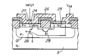
12 a CMOS inverter chip illustrating the invention is
13 shown in Figure 6. According to the invention an
14 N field device is created formed of N+ region 24 and
N+ region 25 as its source and drain, spaced apart and
16 contained from the surface of the substrate in P- well
17 13, which is contained in substrate 9. The input
18 contact to N+ region 24 overlies the insulation in the
19 intermediate region between ~+ regions 24 and 25
forming a field plate 26, and should be metallized to
21 form the field plate of the N field drive.
22 According to the present invention a
23 P+ doped region is contained within P- well 13 from
24 the surface of the substrate, either spaced from or
adjacent N+ region 24. The input is connected to the
26 P+ region 27 at the surface. Also in accordance with
27 the invention N+ region 25 is connected to voltage
28 source Vdd-
29 By the above-described structure, the
input through P+ region 27, is short-circuited to the
31 P- region 13. Therefore the vertical NP~ transistor
32 28, which corresponds to transistor 12 in Figures 2
33 and 5 and has its emitter formed of N+ region 24, its
34 base formed by P- well 13 and its collector formed by
N- substrate 9, has its base and emitter junction
36 short-circuited.
37 The lateral NPN transistor 29 having its
38 - 8 -
..'~
1289Z67
01 emitter formed by N+ region 24, it5 collector by N+
02 region 25 and its base by P- well 13 also has its
03 base-emitter junction short-circuited by means of the
04 P+ doped region 27. The ~+ region 25 also forms in
05 effect a second collector for transistor 28.
06 Since the base and emitter of both
07 transistors 28 and 29 have been effectively
08 short-circuited, no SCR can be formed together with an
09 adjacent PNP transistor such as transistor 8 (Figure
2).
11 However in the case of negative
12 electrostatic discharges into the input, eventually the
13 P+ region 27 becomes debased, due to its inability to
14 supply suf~icient charge carriers. The structure at
this point thus appears as if the P+ region is not
16 present. Once the BVCEO of the lateral bipolar
17 transistor 29 has been reached the structure breaks
18 over, causing conduction between the input, region 25
19 and the power supply Vdd. This has been found to occur
as long as the base resistance of transistor 29 is
21 high, e.g. in excess of about 15,000 ohms per square.
22 This has been found in an experimental device to occur
23 at about 15 volts at the input terminal.
24 For ESD voltages in the positive
direction, the P- well 13 acts as a diode with the
26 N- substrate 9, which is forward biased. However if
27 sufficient voltage is reached again the P+ region 27
28 will be unable to supply sufficient charge carriers,
29 and secondary breakdown occurs.
Since the bases of both of parasitic
31 transistors 28 and 29 are short-circuited to the
32 emitter, latchup in the negative direction is not
33 possible since the possibility of a forward biased
34 junction with each transistor is eliminated, until a
bias of 15 volts or more is placed on the input.
36 Latchup in the positive direction is not possible
37 since the parasitic transistors would be biased in the
38 _ 9 _
:
12~9267
01 reverse direction.
02 While the present invention has been
03 described with reference to an ~- doped substrate
04 using an N field device, it will be recognized by
05 persons understanding this invention that opposite
06 type doping can be used, with a P field device (i.e.
07 an P channel field device).
08 It has been found that the present
09 invention is very effectively utilized where the
substrate is an epitaxial region grown onto a low
11 resistance substrate such as a low resistance antimony
12 doped silicon substrate. The epitaxial layer in a
13 successful prototype was 12 micron, N- type, having
14 10-15 ohm centimetre resistivity. Successful
prototypes were realized using minimum feature widths
16 of 2 and 3 microns in silicon substrate. Conventional
17 processing was used, and the invention can be realized
18 using conventional dopant diffusion steps, oxide
19 isolation and insulation and definition of
metalization conductors.
21 It should be also noted that the present
22 invention reduces the contact injection mechanism
23 referred to in the publication "A CMOS VLSI INPUT
24 PROTECTION DIFIDEW", by C.M. Lin, EOS/ESD SYMPOSIUM
PROCEEDINGS, vol. EOS-6, pp. 202-209, September 1984.
26 In summary, the preferred embodiment of
27 the present invention is protection apparatus for a
28 silicon integrated circuit CMOS inverter comprising a
29 substrate of one polarity type, an opposite polarity
type well within the substrate bounded on a surface of
31 the substrate, a first region within the well of first
32 polarity type bounded on the surface, a region within
33 the well of the opposite polarity type, of greater
34 conductivity than the well, abutting the first
polarity type region and bounded on the surface, a
36 second region within the well of the first polarity
37 type bounded on the surface and spaced from the first
38 - 10 -
-
1289267
01 region and the opposite polarity type region, fir~t
02 conductive apparatus contacting the first region and
03 the opposite polarity region at the surface for
04 connection to an input to the CMOS structure, and
05 second conductive apparatus contacting the second
06 region at the surface for connection to a voltage
07 source of similar polarity as the polarity type as the
08 second region, the first conductve apparatus extending
09 over, but is insulated from, the surface above the
second region, to form a field plate.
11 -- 11 --