Note: Descriptions are shown in the official language in which they were submitted.
1'~89270
PLASMA AMPLIFIED PHOTOELECTRON PROCESS
ENDPOINT DETECTION APPARATUS
sackground of the Invention
~he present invention relates generally to the
field of material processing, and more particularly to
a plasma apparatus and a method for detecting a process
endpoint.
It is desirable to have a non-intrusive, sensitive
etch endpoint apparatus and method to detect the
exposure of a desired sublayer in an item being etched.
Several techniques have been demonstrated for etch
endpoint detection, including optical emission
spectroscopy, plasma impedance monitoring, and laser
interferometry. However, all of these techniques fail
to provide sufficient sensitivity when there is a very
low pattern etch factor, i.e., a low percentage of the
item's surface is exposed to the etching medium.
Additionally, some of these techniques require
considerable signal averaging to improve the
signal-to-noise ratio. The use of these methods thus
results in a slower response to etch plasma
compositional changes and a slower response to endpoint
indicia in the plasma.
The failure of the prior art techniques for
detecting endpoint in the presence of very low pattern
~actors provide a significant impediment to the
semiconductor industry drive for faster circuit
~ devices. Such faster circuit devices require smaller
; component dimensions which often result in very low
wafer pattern densities. At the same time, faster etch
processes result in the need for more precise endpoint
control with a fast endpoint detection response.
Alternatively, it is desirable to be able to
detect with precision the coverage of a low pattern
factor area in a deposition process. Similar detection
problems to those noted above are encountered in this
FI9-87-039 -1- ~ ; - .
,. `,~,.
.. ~ .. ..
~2892~0
type of processing.
The invention as claimed is intended to remedy the
above-described etch endpoint and deposition endpoint
detection problems and limitations that arise when low
pattern factors are present.
The advantages offered by the present invention
are that extremely low pattern factor endpoints can be
detected with high resolution and a very fast response.
This endpoint detection can be utilized when etching,
for example, a top layer through to another layer
therebelow, when those two layers have different work
functions. Likewise, this invention can be used when
depositing a top layer on to another layer, where those
two layers have different work functions. Accordingly,
this invention can be used to detect endpoint when
etching or depositing a top layer of metal,
semiconductor, or insulator material through or on to
another layer therebelow of metal, semiconductor or
insulator material which layer has a different work
function. This invention is particularly advantageous
in that it is essentially independent of the plasma
composition, it has a high detection signal-noise
ratio, and it is not highly wavelength sensitive.
Summarv of the Invention
Briefly, one aspect of the invention comprises a
plasma processing apparatus including
a plasma chamber for processing an item that
includes a first portion of a first material and a
second portion of a second material, with the
~ 30 first and second materials having different work
functions;
means for generating a plasma in the plasma ~-~
chamber, the plasma generating means including an
RF-powered electrode excited by an RF excitation
frequency;
means for generating and ejecting electrons
only when the second material is exposed to the
FI9-87-039 -2-
. ~i~.~..
- " .
r:: ~
12~39270
plasma;
means for increasing the energies of the
generated electrons and accelerating the electrons
into the plasma, with sufficient energy to thereby
generate a secondary electrons in the plasma;
means for receiving a plasma RF discharge
voltage signal;
means for filtering the plasma RF discharge
voltage signal to remove the RF excitation
frequency therefrom; and
means for amplifying the natural frequencies
of the plasma discharge in response to the
electron perturbation in the plasma discharge
voltage signal to thereby detect the processing
endpoint or a surface condition.
In a preferred embodiment, the electron energy
increasing and accelerating means comprises means for
generating an electrode voltage sheath, and means for
generating the electrons within this voltage sheath to
thereby accelerate the electrons into the plasma.
In a further aspect of this embodiment, the
electron generating means may comprise means for
directing a beam of photons in a selected energy range
onto the item, which energy range is not sufficient to
eject photoelectrons from the first material, but is
high enough to generate photoelectrons from areas of
exposed second material. This photon beam directing
means may comprise means for generating laser pulses.
In a further embodiment of the present invention,
the filtering means may comprise a capacitor for
blocking out any DC signal components, and notch filter
means for removing the harmonics of the RF excitation
signal.
The present apparatus may further comprise means
for integrating the filtered signal. In one
embodiment, this integrating means may include means
for detecting the filtered signal a predetermined time
period after the occurrence of each laser pulse and
FI9-87-039 -3_
` i~t~
. .
'~ ~
~289270
integrating a plurality of the detected filtered
signals.
In a further aspect of the present invention, a
method is disclosed and claimed for detecting the
endpoint in a plasma etching or deposition process.
This method~comprises the steps of
disposing an item to be processed in a plasma
chamber, th-e item including a first portion of a first
material and a second portion of a second material,
with the first and second materials having different
work functions;
generating by means of an RF electrode
excited by an RF excitation frequency a plasma in
the plasma chamber to process the item;
generating and ejecting electrons from the
material only when the second material is exposed
to the plasma;
accelerating the generated electrons into the
plasma with a sufficient energy to thereby
generate secondary electrons in the plasma;
receiving a plasma discharge voltage signal;
and
filtering and amplifying the plasma discharge
voltage signal to monitor the natural frequencies
of excitation and decay of the discharge plasma,
to thereby determine the process endpoint or
surface condition.
Brief Description of the Drawinqs
Fig. l is a schematic block diagram of one0 embodiment of the present invention.
Fig. 2 is a schematic circuit diagram of a filter
and amplifier network which may be utilized to
implement the filter and amplifier block~ of Fig. 1.
Fig. 3 is a graphical representatiOn of an
integrated signal response obtained by utilizing the
apparatus and method of the present invention.
FI9-87-039 -4-
. ., j ,. ..
1289270
Detailed Description of the Preferred Embodiment
The present invention is based on the use of the
photoelectric effect, i.e., the fact that when an
energy beam is directed at a material surface where the
energy per quantum which is greater than the work
function for that material, then electrons will be
ejected from that surface. It was recognized that in
an etching process for etching, for example, a top
layer of a first material through to a second layer
therebelow of a second material, the work functions of
those two materials will differ in almost every case.
Likewise, in a deposition process, it was recognized
that in the deposition of a top layer of a first
material on to a second layer of a second material, the
work functions of these two materials will differ in
almost every case. The present invention utilizes the
electron-ejection effect in combination with this
realization of the differing work functions for these
two layers of material on the item being processed to
form an operable endpoint detection apparatus and
method. Additionally, the invention resides in the use
of means to increase the energy of electrons ei`ected
when a given material is exposed and to accelerate
those electrons into the plasma with sufficient energy
to generate detectable secondary electrons. Finally,
the present invention resides in the discovery that the
response to these secondary electronc in the etching
plasma may be de~ected at the natural frequencies of
excitation and decay of the plasma discharge.
Accordingly, the RF plasma excitation frequency and its
harmonics, and the DC components in the excitation
signal may be removed by appropriate filtering, while
the band of frequencies containing the natural
frequencies of excitation and decay of the plasma
3s discharge is amplified to obtain a highly enhanced
signal/noise ratio.
The present invention will first be described in
the context of an etching system. However, the
FI9-87-039 -5-
i2~39270
invention applies equally to deposition and other
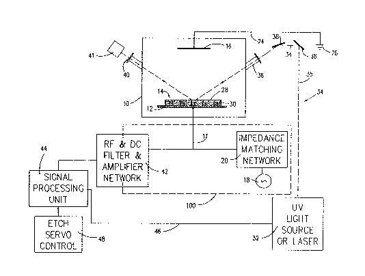
processing systems. Referring now to Fig. 1, there is
shown a standard dry etching chamber 10 with an
electrode 12 upon which an item 14 to be etched is
disposed. This item 14 being etched may comprise, by
way of example, a top or a first layer 28 of a first
material disposed over a second layer 30 of a second
material, with the first and second materials having
different work functions. (In Fig. 1, the second layer
comprises the studs 30.) In the example shown in Fig.
1, this item to be etched may be a wafer 14. By way of
example, and not by way of limitation, a typical dry
etching chamber that may be utilized to perform
reactive ion etching is described in the reference L.
M. Ephrath, "Dry Etching for VLSI - A Review", in
Semiconductor Silicon 1981, (eds. H. R. Huff, Y.
Takeishi and R. J. Kriegler), The Electronchemical
Society, Pennington, NJ, Vol. 81-5, pp. 627 (1981).
Such a chamber would have gas inlets in order to
provide an appropriate etching gas mixture for the
chamber 10.
The RF electrode 12 in the chamber 10 is connected
by means of an electrical line 17 to a standard RF
source of energy 18. The RF energy source 18 provides
an excitation frequency to excite the gases in the
chamber to form an etching plasma therein. The RF
excitation frequency from the RF excitation signal
source 18 is provided to the electrode 12 by means of
an impedance matching network 20. By way of example,
and not by way of limitation, this impedance matching
network 20 may be implemented by a standard LC or Pi
circuit of the type shown in the reference A. J.
Diefenderfer, Principles of Electronic Instrumentation,
W. B. Saunders Co, Philadelphia, PA (1979). A second
electrode 16 is disposed on the opposite side of the
chamber from the electrode 12 and is connected by means
of a line 24 to a reference potential 26. The RIE
etching plasma is generated in the volume between the
.
FI9-87-039 -6-
lZ89270
electrodes 12 and 16.
The invention further comprises means for
generating and ejecting electrons only when a selected
material is exposed to the etching plasma. In one
embodiment, the means for generating electrons
comprises means for directing a beam of energy of
either photons or particles in a selected energy range
onto the surface of the item 14 being etched. This
energy range is not sufficient to eject electrons from
one of the first material layer 28 or the second
material layer 30 on the item 14 being etched, but is
high enough to eject electrons from the other of the
first material layer 28 or the second material layer
30, to thereby eject electrons when the other material
is exposed.
In the embodiment shown in Fig. 1, the energy beam
directing means comprises an energy beam source 32, an
energy beam 34 following a path 35, and a window 36
into the chamber 10 to permit application of the energy
beam onto the surface of the item 14 being etched. In
this embodiment, the energy beam source may be
comprised simply of a laser or a UV light source. An
ultraviolet wavelength laser such as an excimer laser,
or a frequency-quadrupled Nd:VAG laser, or a
frequency-doubled tunable dye laser may also be
utilized, for example. Conveniently, the energy beam
source should be a pulsed source or a continuous wave
source that is appropriately chopped. The energy beam
path 34 may include one or more mirrors 38, as
required, in order to direct the energy beam through
the window 36 and into the chamber 10. This energy
beam may be focussed or unfocused, depending on the
amount of area that is to be impinged on the item 14
being etched. It may be desirable to also include a
window 40 in the chamber 10 and an energy beam stop 41
to receive the energy beam after it is reflected off of
the surface of the item 14 to prevent the beam from
making uncontrolled reflections within the chamber 10.
FI9-87-039 -7-
~289270
It should be noted that the energy beam may be directed
normal to the item 14 being etched, or it may be
directed at an oblique angle to the item 14 being
etched. It should also be noted that the more oblique
the angle of incidence of the energy beam onto the
surface of the item 14, the more generalized will be
the measurement for the endpoint.
In the example of Fig. l, when the energy beam 34
strikes a metal, semiconductor, or insulator surface,
it will eject photoelectrons if the photon energy
exceeds the work function, U, of the material. The
ejected photoelectrons will have an energy, KEel, equal
to: KEel = hv-U, where hv is the energy of the
incident light. However, if the photon energy in the
energy beam is less than the work function for the
material, then no photoelectrons will be ejected,
regardless of the intensity of the energy beam.
Accordingly, the energy of the energy beam is chosen so
that it does not eject electrons from one of the first
or second materials on the item 14, but does eject
electrons from the other of the first or second
materials. By way of example, assume that the first
layer 28 of first material comprises a layer of an
insulator such as glass, polyimide, or silicon dioxide,
while the second layer 30 of second material comprises
a metal. The use of a laser which generates a UV light
in the range of 230 - 250 nm results in a photon energy
of between 5.4 to 4.9 eV, respectively. A typical
metal work function is 4.3 to 4.5 eV, while a typical
work function for an insulator such as silicon dioxide
is on the order of 9-10 eV. Thus the direction of an
ultraviolet energy beam to strike the first layer 28 of
silicon dioxide will not eject photoelectrons.
However, when small areas of metal become exposed
during the etching process, these exposed metal areas
will eject photoelectrons with an energy of between 0.6
to 0.8 eV, depending on the wavelength of the light and
the exact value of the work function for the material.
FI9-87-039 -8-
12~39270
These photoelectrons thus are characterized by a low
kinetic energy and insufficient energy to produce
secondary ions by collisional processes.
However, the present invention further includes
means for increasing the energies of these low kinetic
energy photoelectrons and accelerating them with a
sufficient energy into the etching plasma to generate
secondary electrons in the plasma. In a preferred
embodiment, this photoelectron energy increasing and
accelerating means comprises means for generating an
electrode voltage sheath, and means for generating
these low kinetic energy photoelectrons within this
voltage sheath to thereby accelerate the photoelectrons
into the plasma. In the embodiment shown in Fig. l,
the photoelectron energy increasing and accelerating
means is implemented by disposing the item 14 being
etched on the RF cathode electrode l2 or the RF anode
electrode l6 during the etching operation. The sheath
voltage for these electrodes is determined by the input
electrode power density and the gas composition and
pressure in the etching chamber lO. For example, the
RF cathode electrode 12 will typically generate`a
sheath voltage of lO0 eV to l KeV either in a batch RIE
tool using a 0.25 W/cm 2 electrode power density at a
pressure of 50 mTorr, or in a single wafer etch tool
using a l-2W/cm2 electrode power density and at a
pressure of 0.5-4 Torr. The anode electrode 16 will
typically have a sheath voltage of on the order of
30-500 volts for those excitation levels. Thus, in the
example shown in Fig. l with the item 14 disposed on
the cathode electrode l2, any low kinetic
photoelectrons produced are ejected within the cathode
sheath voltage disposed around the cathode electrode
12. Accordingly, these low kinetic energy ejected
photoelectrons are accelerated by the strong potential
field in the cathode sheath. The photoelectrons are
accelerated across the sheath, gaining considerable
kinetic energy from the electrostatic interaction of
FI9-87-039 -9-
~ ,
" ' 1289270 ``)
the electrons with the sheath field so that the
photoelectrons are accelerated close to the sheath
potential, which, as noted previously, ranges from 100
eV to 1 KeV. Accordingly, these low kinetic
photoelectrons are converted to high energy electrons
which are accelerated into the plasma between the
electrodes 12 and 16. In the plasma, these high energy
electrons have sufficient energy to induce secondary
electrons from collisions with gas phase species.
Additionally, these high energy photoelectrons can
strike the opposite electrode 16 and produce secondary
electrons from that surface. The net result of this
generation of secondary electrons is the ampliication
of the photoelectron ejection phenomena.
If laser pulses are utilized as the energy beam
source 32 to produce the primary photoelectrons, a
repetitious perturbation of the plasma discharge
impedance in the chamber results from the pulsed influx
of high energy electrons following each laser shot
(assuming an appropriate work function material has
been exposed). This amplified repetitious perturbation
of the plasma discharge impedance and voltage is caused
by the sudden change in the current at the RF electrode
as the high energy electrons are ejected into and
amplified (by an increase in secondary ejections) by
the plasma. Since the RF electrode 12 and the plasma
are electrically coupled, this perturbation results in
an oscillation which dampens out in time. It has been
discovered that this amplified repetitious perturbation
of the plasma discharge voltage may be monitored
~ electronically with a high signal/noise ratio, by
filtering out the RF excitation frequency (usually
13.56 MHz) along with any RF excitation frequency
harmonics and DC components of the signal detected at
the RF powered electrode 12, while amplifying the
frequencies of excitation and decay of the plasma
discharge perturbation.
In order to detect and measure this plasma
FI9-87-039 -10-
i289270
perturbation, the RF electrode 12 may be connected to a
filter and amplifier network 42 to remove unwanted
frequencies and to amplify desired frequencies. In
this regard, applicants have discovered that the major
S response from this plasma perturbation is in the
natural frequencies of excitation and decay of the
plasma discharge (the inverse of the decay time
constant). Accordingly, a series of bandpass and
blocking filters may be utilized to remove the RF
fundamental excitation frequency, associated RF
excitation frequency harmonics, and the DC self-biased
voltage of the cathode 12. Note that in some
applications, a set of LC networks may be combined with
a low pass filter and a DC blocking capacitor in order
to accomplish the desired filtering function. In other
applications with high RF power, commercially available
blocking networks may be required. Means are also
provided for amplifying the natural frequencies of the
excitation and decay of the plasma discharge in the
plasma discharge voltage signal,i.e., amplifying the
photoelectric signal by tuning the amplification
response of the filter to match the excitation and
decay frequencies.
After the removal of the undesirable DC and RF
components from the electrode signal and the
amplification of the natural frequencies of decay of
the plasma discharge voltage perturbation, tnis
filtered and amplified cignal is applied to a signal
processing unit 44. In one embodiment, this signal
processing unit may simply comprise an oscilloscope.
- For a quantitative measurement, this signal processing
unit 44 may comprise means for integrating the filtered
and amplified signal in synchronization with the laser
pulses from the energy beam source 32. This
synchronization can be obtained by means of a
synchronization signal via the line 46. In essence,
the signal processing unit operates in accordance with
the synchronization signal on line 46 to detect the
FI9-87-039 -11-
. , ~
~ '
~289;~70
filtered signal at a series of predetermined times
after the occurrence of each laser pulse, and then to
integrate these detected filtered signals over a
plurality of laser pulses. A typical signal processing
unit which may be utilized to integrate the signal
comprises a boxcar integrator circuit. Such a boxcar
integrator could be set, for example, to detect the
filtered an-d amplified signal over a series of selected
time-windows occurring at a series of different
selected times after a given laser pulse, and then to
integrate each of these different time-window signals
over a series of laser pulses. A standard time-window
period might be, for example, l microsecond and the
number of laser shots that may be integrated might be
in the range of 5 - lO0. Alternatively, the signal
processing unit 44 may be implemented by means of a
transient digitizer. In essence, in this preferred
embodiment the sudden appearance of lO0 KHz to 3MHz
damped oscillations in phase with the laser shots at
the output of the signal processing unit 44 indicates
that the endpoint has been reached and/or signals the
appearance of the low work function material.
The output from the signal processing unit 44
could be applied to an etch servo control unit 48 for
controlling an etching parameter (RF power, gas flow)
in the chamber 10, or for stopping the etching process
when a predetermined signal level is detected by the
signal processing unit 44. Some form of threshold
detection unit might be included in the control block
48 to facilitate this operation. A similar servo
control unit could be used to control a deposition
parameter. Alternatively, the block 48 could simply
comprise a chart recorder unit. -~
Referring now to Fig. 3, there is shown a typical
integrated plasma perturbation response as seen at the
output of the signal processing unit 44 when low
kinetic energy photoelectron pulses have been amplified
by an etching plasma. It can be seen that in this
FI9-87-039 -12-
` :,h`~,.;;
1289270
graph, the time axis is in microseconds and the voltage
axis is in millivolts. The points in the graph
represent a series of integrated time-windows occurring
after a series of laser pulses. 40 laser shots were
integrated in order to form each point in the time
graph.
Referring now to Fig. 2, there is shown one
example of a filter and amplifier network for removing
various undesirable frequencies from the plasma
discharge perturbation signal and for amplifying the
frequencies of excitation and decay of the plasma
discharge which may be utilized to implement the filter
and amplifier network 40. In this embodiment, the
electrode 12 is connected via line 16 to an optional
capacitive divider network 50 for reducing the plasma
discharge signal voltage to a desired voltage range.
In the embodiment shown in Fig. 2, this divider network
simply comprises the capacitors 52 and 54 connected in
electrical series between the line 16 and a reference
potential such as ground potential. A reduced voltage
in the desired voltage range is taken from a node 56
disposed at the connecting point between the capacitors
52 and 54.
The circuit further includes means for blocking
any DC components in the plasma discharge signal. This
DC blocking function is accomplished in Fig. 2 simply
by connecting a DC blocking capacitor 58 to the node 56
at one end thereof.
The circuit further includes means for removing
the fundamental RF excitation signal from the plasma
~ disc~arge impe~ance signal. In the embodiment shown in
Fig. 2, this means is implemented simply by a notch
filter 60 connected to the other end of the DC blocking
capacitor 58 at node 59. The notch filter 60 comprises
an inductor 62 connected in parallel to a capacitor 64,
with the resulting notch filter designed to be in
resonance with the RF drive frequency of approximately
13.56 M~z. In the embodiment of the present invention
FI9-87-039 -13-
'```:'
, ~
. :
i289270
shown in Figs. 1 and 2, the notch filter 60, the DC
blocking capacitor 58, the capacitive voltage divider
network S0, the impedance matching network 20, and the
RF signal source 18 are all disposed within a ground
shield 100. Because of the potential for high RF
voltages at- the notch filter 60, a wire wound inductor -
62 is utilized in this filter.
The circuit further includes means for amplifying
the range of frequencies including the frequencies of
decay of the plasma discharge perturbation. A variety
of different amplifiers may be utilized to perform this
amplification function. In the embodiment shown in
Fig. 2, this amplification function is accomplished by
connecting node 66, at the other end of the notch
filter 60, to the reference potential via a capacitor
68. For frequency components in the filtered plasma
discharge signal which are below the resonance
frequency for the notch filter 60, the notch filter
acts as an inductor. Accordingly, the notch filter 60
in combination with the capacitor 68 is designed to be
in resonance for a band of these lower frequencies to
thereby increase or peak the amplitude of the signa} in
this frequency range. By way of example, the notch
filter 60-capacitor 68 combination could be designed to
amplify signal frequencies in the range of 0.3-7 MHz,
and preferably 1-5 MHz.
In the alternative, if the drive frequency is
below the perturbation frequencies to be amplified, then
inductor elements could be substituted for the
capacitors 68 and 78 in Fig. 2 to effect signal
- amplification.
The circuit may further include a second
lower-voltage notch filter 70 disposed outside of the
ground shield 100 for removing any pick-up of the RF
excitation frequency fundamental in the low RF
environment. This notch filter is connected at one end
to the node 66, and again may comprise a
parallel-connected inductor 72 and capacitor 74
FI9-87-039 -14-
* . ~ ~ .
.. . .
.... i .
1289270
designed to be in resonance at approximately 13.56 MHz.
Again, the node 76 at the other end of the second notch
filter 70 may be connected to the reference voltage via
a capacitor 78 to form a second amplifier. The
inductive notch filter 70 in combination with capacitor
78 again is designed to be in resonance for a band of
frequencies below the 13.56 MHz notch of the filter 70
to thereby increase or peak the amplitude of the signal
in this frequency range.
The circuit further includes means 80 connected to
node 76 for filtering out any harmonics of the RF
excitation frequency fundamental. In the example
embodiment shown in Fig. 2, the harmonic filtering
means comprises a resistor 82 connected between node 76
and a node 84, and a capacitor 86 connected between the
node 84 and the reference potential.
Finally, the circuit may include an optional fuse
circuit 88.
Photoelectrons will be ejected from a given
substrate material if the incident light energy exceeds
the work function of the substrate material.
Accordingly, a laser beam energy may be tailore`d to a
wide variety o~ first and second materials on the item
being etched. The only requirement is that the two
materials have different work functions. Typical
examples in which this process may be utilized comprise
the etching of an insulator material such as glass,
quartz, or polyimide with typically high work functions
of on the order of 9 - 10 eV, with a second layer
therebelow of a lower work function material such as a
metal (with a work function in the range of 4.3 - 4.5
eV), or a semiconductor (with a work function in the
range of 4.2). When an energy beam with a selected
energy which is less than the work function for the
insulator material, but greater than the work function
energy for the material layer therebelow is incident on
the insulators, then the energy beam will not eject
photoelectrons at the outset of the etching process.
FI9-87-039 -15-
.~
. .. ~.
.:
.
1289270
However, when the energy beam is incident on exposed
metal, (e.g., AlCu, Au, or W) or incident on a silicon
surface, then photoelectrons will be ejected from the
surface and accelerated by the sheath field to produce
a plasma perturbation.
In-th~ alternative, the low energy work function
material may be disposed as the top layer over the
second laye-r of a higher work function material. In
this instance, a plasma perturbation signal would be
received until the lower work function material has
been etched away. This plasma perturbation would then
significantly decrease and this change in the plasma
perturbation could be monitored and used to determine
endpoint.
Additionally, the present apparatus ana technique
is sensitive to silicon and may be used for the
endpoint detection of heavily doped silicon regions
over or under materials such a polysilicon. In this
regard, N+ silicon disposed below polysilicon is
generally very difficult to detect by other diagnostic
techniques, especially where low pattern factors of the
type found with advanced transistors are present.
However, since the Fermi levels are much different
between N+ silicon and polysilicon, the work functions
for these materials also differ, with the work function
of the N+ silicon being lower. Accordingly, the use of
a frequency-doubled tunable dye laser may be used to
emit photoelectrons from the N+ silicon but not from
the polysilicon, thereby providing an endpoint
detection facility.
~ As a further point, it has been determined that
the present apparatus and method is highly sensitive to
the surface composition of silicon during plasma ;~
etching. In particular, the present apparatus and
technique can detect in-situ, during plasma processing,
the presence of surface contaminants or extremely thin
deposited layers disposed over silicon. Such layers
form an effective barrier to photoelectron penetration,
FI9-87-039 -16-
~289270
and thus result in a change in the observed
photoelectric signal. Since other in situ techniques,
such as laser interferometry, require much greater film
thicknesses before detection is possible, the present
apparatus and method offer considerable advantage in
sensitivity for use in an in-situ surface analysis
technique. Conventional surface monitoring techniques,
such as X-ray photoelectron spectroscopy, or auger
spectroscopy are highly surface sensitive, but the use
of these techniques requires the transfer of the wafer
to an ultra-high vacuum environment and so may only be
employed for post-process analysis after the etching
process is complete. Accordingly, the present
apparatus and method is advantageous for the
measurement and detection of surface contaminants or
sputter deposited films during the actual plasma
exposure period.
Note that the present structure can be used
generally to detect the ur.iform deposition of a layer
over an electron emitting layer. In this case, there
would be an initial signal generated by the generation
of secondary electrons in the plasma. This signal
would disappear when a uniform layer was deposited over
the electron emitting material.
The present etching apparatus has been discussed
in the context of an item with a first layer of a first
material disposed in a vertical relationship with a
,se~ond layer of a second material. However, the
invention is not limited for use in etching items with
this configuration. In this regard, a first portion of
" a first material and a second portion of a second
material may be disposed in different lateral locations
on the item to be etched, and not directly over each
other. This first and second material relationship
could be used to determine endpoint.
The present invention is based on the appropriate
tuning of the,photoelectric effect to the work
functions of the materials being etched to thereby
FI9-87-039 -17-
....
~289270
generate low kinetic energy photoelectrons, in
combination with an accelerating apparatus which will
accelerate these low kinetic photoelectrons and convert
them into high energy photoelectrons which will
generate secondary electron emission in the plasma. In
the present-embodiment qf the invention, the foregoing
concepts are implemented by generating the
photoelectrons within the sheath field for one of the
RF electrodes. The sheath field amplifies the energy
of the photoelectrons in an amount sufficient to induce
secondary ionization in the plasma. It is this large
number of secondary electrons combined with the primary
photoelectrons which ultimately produces a detectable
plasma perturbation. A further important aspect of
the present invention is the recognition that the
plasma perturbation signal primarily resides in the
natural frequencies of excitation and decay of the
plasma discharge (the inverse of the excitation and
decay time constant of the perturbation). The present
invention includes appropriate filtering and detecting
apparatus in order to implement this aspect of the
invention.
The present endpoint detection apparatus and
method is direct, relatively low cost, and can be
installed on existing equipment with minimal
modifications. In this regard, only a single window
port is required in the chamber in order to permit a
laser beam to be directed onto the it:em being etched.
Alternatively, an optical fiber or waveguide can be
f 30 used in order to transmit the laser beam into the
~ etching chamber. Detection of the resulting plasma
perturbation may be accomplished simply by attaching
electrical filters to the RF match box circuit and
feeding the filtered output to an analog detector. It
should be noted that a single laser can be utilized to
provide power to operate multiple reactors, since only
approximately one mJ/pulse is necessary (a typical
excimer laser produces lO0-lO00 mJ/pulse). This
FI9-87-039 -18-
~ ` `,;'. ~'f'~`'``^
1289270
technique can provide endpoint detection for future and
existing process steps in which all other prior art
techniques fail, and thus may play a critical role in
future semiconductor technology processing.
The present technique and apparatus was
succ~ssfully demonstrated on low pattern factor product
wafers comprising a first layer of an insulating
material disposed over Al/Cu vias. The signal/noise
ratio of the measured optogalvanic signal was
determined to be greater than 20:1, indicating a very
high sensitivity. In this demonstration, the
semiconductor wafer being etched had a 5% via hole
pattern, with the balance being SiO2. No measurable
photoelectric signal was derived from the blanket SiO2
wafers.
It should be noted that the present apparatus and
method is not highly wavelength sensitive as compared
to other techniques, such as, for example,
laser-induced fluorescence. Accordingly, a chopped
incoherent UV light source may be used in place of the
laser. Examples of other alternative light sources
include mercury arc lamps, and hydrogen or Xenon
discharge lamps.
Additionally, it should be noted that the present
apparatus and technique is only weakly dependent on the
composition of the plasma, and SG has an extremely
broad base, or window, of operat.on.
While the present invention has been particularly
shown and described with reference to preferred
embodiments therefore, it will be understood by those
skilled in the art that the foregoing and other changes
inform and detail may be made therein without departing
from the scope and the spirit of the present invention.
FI9-87-039 -19-
r .