Language selection

Search

Patent 1289273 Summary

Third-party information liability

Some of the information on this Web page has been provided by external sources. The Government of Canada is not responsible for the accuracy, reliability or currency of the information supplied by external sources. Users wishing to rely upon this information should consult directly with the source of the information. Content provided by external sources is not subject to official languages, privacy and accessibility requirements.

Claims and Abstract availability

Any discrepancies in the text and image of the Claims and Abstract are due to differing posting times. Text of the Claims and Abstract are posted:

  • At the time the application is open to public inspection;
  • At the time of issue of the patent (grant).
(12) Patent: (11) CA 1289273
(21) Application Number: 1289273
(54) English Title: RADIATION DETECTOR
(54) French Title: DETECTEUR DE RAYONNEMENT
Status: Term Expired - Post Grant
Bibliographic Data
(51) International Patent Classification (IPC):
  • G1T 1/20 (2006.01)
  • G1T 1/02 (2006.01)
  • G1T 1/24 (2006.01)
(72) Inventors :
  • BURGESS, PETER HAMILTON (United Kingdom)
(73) Owners :
  • HEALTH PROTECTION AGENCY
(71) Applicants :
  • HEALTH PROTECTION AGENCY (United Kingdom)
(74) Agent: GOWLING WLG (CANADA) LLP
(74) Associate agent:
(45) Issued: 1991-09-17
(22) Filed Date: 1987-11-04
Availability of licence: N/A
Dedicated to the Public: N/A
(25) Language of filing: English

Patent Cooperation Treaty (PCT): No

(30) Application Priority Data:
Application No. Country/Territory Date
8605394 (United Kingdom) 1986-03-05

Abstracts

English Abstract


ABSTRACT
RADIATION DETECTOR
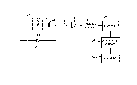
A radiation meter comprises two p-i-n photo-
diodes (1,3) each disposed to operate in a self-
biasing mode. The larger diode has an attenuating
shield (33) and the outputs of the diodes are
combined. The invention is intended for active
personal dose meters for the same general purpose as
Geiger-Muller tubes.


Claims

Note: Claims are shown in the official language in which they were submitted.


- 6 - 27975-3
THE EMBODIMENTS OF THE INVENTION IN WHICH AN EXCLUSIVE
PROPERTY OR PRIVILEGE IS CLAIMED ARE DEFINED AS FOLLOWS:
1. A radiation detector for generating pulses in response
to incident radiation, comprising: first and second photo diodes,
said first photo diode having a substantially larger effective
sensitive area than that of the second diode; means for
attenuating radiation incident on said first diode; and means for
combining the output of said first and second diodes.
2. A radiation detector according to claim 1, wherein the
said means for attenuating comprises a thin metallic member.
3. A radiation detector according to claim 1, further
comprising means for reducing the amplitude of pulses produced by
the said first diode.
4. A radiation detector according to claim 3 in which the
said means for reducing comprises a capacitor electrically in
series with the said first diode.
5. A radiation detector according to claim 1, further
comprising means for counting pulses which exceed a threshold in
the said output.
6. A radiation detector according to claim 1 wherein each
of said photo diodes is a PIN diode.

- 7 - 27975-3
7. A radiation detector according to claim 6 wherein said
diodes operate in a self biassing mode.

Description

Note: Descriptions are shown in the official language in which they were submitted.


1~89;:73
- 1 - 27975-3
"RADIATION DETECTOR"
BACKGROUND OF THE INVENTION
The present invention relates to a radiation detector
which is particularly though not exclusively intended for use in
dosemeters, for example small, active personal dosemeters for the
same general purposes as Geiger Muller tubes.
The object of the present invention is to provide novel,
and at least in some respects, improved detection of radiation.
SUMMARY OF THE INVENTION
According to a broad aspect of the invention there is
provlded a radiation detector for generating pulses in response to
incldent radiation, comprising: first and second photo diodes,
said first photo dlode having a substantially larger effective
sensitive area than that of the second diode; means for
attenuating radiation incident on said first diode; and means for
combining the output of said first and second diodes.
Preferably the diodes are selected such that the
variation of output with incident radiation is compensated by the
output from the other. There may be provided means for reducing
the amplitude of pulses produced by the larger diode; this means
may comprise a capacitor in series with that diode.
The aforementioned means for attenuating may comprise a
metallic screen, preferably in the form of a brass cap or shield.

C~ ~289~273
- 2 -
BRI~F DESCRIPTION OF T~E DRAWINGS
Figure 1 illustrstes schematically a
raaiation meter incorporating a detector according to
the invention; and
Figure 2 illustrates one possible physical
configuration of the components in the meter
according to Figure 1.
l)TAIL~D I~ESCR IPT ION
Figure 1 illustrates by way of example a
circuit comprisin~ a detector, constituted in this
embodiment by two silicon PIN photodiodes 1 and 3,
together with other circuit elements forming a
complete meter. In this particular embodiment of
the invention the other elements comprise a capacitor
4 in series with the diode 1, a preamplifier 5 which
is arranged to receive the combined output of the
diodes l and 3, an amplifier 6, a threshold detector
7, ana a counter and timer 8, the elements 5 to 8
constituting, in this embodiment, a means for
indicating the rate of pulses which exceea a
threshold. The counter may be coupled to a
processing circuit 9, whicn in known manner may
produce denoting the dose rate and the total dose and
provide an alarm signal if either the dose rate or
the dose exceeds a threshold. TAese signals may
control respective sections of a display device 10
(such as a liquid crystal display).
Considering first the diode l, which is
preferably a silicon photodiode having an intrinsic
layer between appropriately doped P and N regions, it
will be understood that photon radiation incident on
the diode can ~enerate energetic electrons from
photoelectric and Compton interactions with the
silicon crystal lattice. Sucn electrons then lose
energy by interaction with tAe crystal lattice and
can generate electron-hole pairs within the intrinsic
- '

~289273
layer. The electrons thus generated are separated
by the inherent field within the device to form a
charge pulse which can be amplified by the
preamplifier 5 and the amplifier 6. In this
embodiment of the invention, if the charge pulse is
in excess of said threshold as determined by the
threshold detector 7, the pulse may be counted.
Although a device employing only a single
PIN diode in a self-~iassing moae has some utility,
it exhibits a response which is substantially
non-uniform with variation in radiation energy and it
is preferable to provide compensation by means of at
least one further diode in order to obtain a combined
output which is substantially uniform with variation
of radiation energy. For this purpose the diode 1,
which may be a BPX61 PIN diode, is provided with
means for attenuating incident radiation, preferably
constituted by a brass cap, typically of the order of
2.5 millimeters thick. The cap is schematically
illustrated in Figure 1 by the dashed line 2. The
provision of such a cap would normally result in a
large underestimate for radiations of energy less
than, for example, 150 keV. To compensate for this
the output from a smaller diode 3 is added to that
from the larger diode 1. The diode 3, which may be
a ~PX65 PIN diode of which the glass lens is removed
to improve the low energy response, may have, for
example, approximately 14~ of the effectively
sensitive area of the diode 1. In addition, a
capacitor 4 may be disposed electrically in series
with the-diode 1 so as to reduce the~signal amplitude
; ~ from the diode 1. In this manner the falling
output, from the larger diode, combined with the
rising output, from the smaller diode, produces a
response which is substantially uniform with respect
to radiation energy. For the particular examples of
,

~;~89273
diode as stated above, the capacitor may be a 180pF
capacitor.
Figure 2 illustrates by way of example the
physical arrangement of a meter 11 which is
electrically arranged according to Pigure 1. The
diodes 1 ana 3 may be incorporated into an integrated
circuit 12, which contains all the detection,
amplifying and processing stages of the device.
The iarger of the two diodes is covered by
the brass shield 2. The two diodes should be
mounted at least 6mm apart to reduce shadowing by the
brass shield 2 of the unshielded diode 3 from low
energy radiation. The surface of the integrated
circuit in which the diodes are incorporated faces
away from the body of the wearer. Tne shield may
comprise a disc which is mounted centrally over the
aiode 1 and is of significantly larger area than the
active area of the diode 1. This configuration has
in essence the same properties 8S the shield
described with reference to Figure 1. The display
10, is preferably mounted in the top face of tne
meter for the sake of good visibility. If desired
an audible alarm device 13 (driven by the circuit 9
which is incorporated in the integrated circuit 12
may be disposed adjacent the display 10 and may be
triggered by the alarm signal. A battery 14,
preferably of sufficient capacity to last at least
one year, may be disposed in a recess at the bottom
of the meter.
A ~etector as described may readily be
arranged to provide a pulse output which at a
- ~ suitable threshold is substantially independent of
photon energy and angle of incidence for photqns of
energy greater than approximately 40 keV. Such a
device has a sensitivity suitable for employment of
the device in an active personal dosemeter.
,
: ~ .
'' ' ,: ` ' ` .
: ' '
,

89273
A detector as described is capable of
providing improved energy response and polar response
with respect to known energy compensated Geiger
Muller tubes and offer further the advantages of
robustness, consistency, cheapness of ease of
manufacture and a more accurate background response,
in addition to avoiding any need for high volta~e
electrical supplies.
-
: 25
. ., ~, . . . . . .. . ... .. .. .. ... . . .. .. .. .
'

Representative Drawing
A single figure which represents the drawing illustrating the invention.
Administrative Status

2024-08-01:As part of the Next Generation Patents (NGP) transition, the Canadian Patents Database (CPD) now contains a more detailed Event History, which replicates the Event Log of our new back-office solution.

Please note that "Inactive:" events refers to events no longer in use in our new back-office solution.

For a clearer understanding of the status of the application/patent presented on this page, the site Disclaimer , as well as the definitions for Patent , Event History , Maintenance Fee  and Payment History  should be consulted.

Event History

Description Date
Inactive: Expired (old Act Patent) latest possible expiry date 2008-09-17
Inactive: IPC from MCD 2006-03-11
Letter Sent 2005-09-23
Revocation of Agent Requirements Determined Compliant 2005-05-30
Appointment of Agent Requirements Determined Compliant 2005-05-30
Inactive: Office letter 2005-05-30
Inactive: Late MF processed 2004-10-04
Letter Sent 2004-09-17
Inactive: Late MF processed 2004-02-10
Letter Sent 2003-09-17
Grant by Issuance 1991-09-17

Abandonment History

There is no abandonment history.

Owners on Record

Note: Records showing the ownership history in alphabetical order.

Current Owners on Record
HEALTH PROTECTION AGENCY
Past Owners on Record
PETER HAMILTON BURGESS
Past Owners that do not appear in the "Owners on Record" listing will appear in other documentation within the application.
Documents

To view selected files, please enter reCAPTCHA code :


To view images, click a link in the Document Description column (Temporarily unavailable). To download the documents, select one or more checkboxes in the first column and then click the "Download Selected in PDF format (Zip Archive)" or the "Download Selected as Single PDF" button.

List of published and non-published patent-specific documents on the CPD .

If you have any difficulty accessing content, you can call the Client Service Centre at 1-866-997-1936 or send them an e-mail at CIPO Client Service Centre.

({010=All Documents, 020=As Filed, 030=As Open to Public Inspection, 040=At Issuance, 050=Examination, 060=Incoming Correspondence, 070=Miscellaneous, 080=Outgoing Correspondence, 090=Payment})


Document
Description 
Date
(yyyy-mm-dd) 
Number of pages   Size of Image (KB) 
Abstract 1993-10-21 1 12
Claims 1993-10-21 2 29
Drawings 1993-10-21 1 11
Descriptions 1993-10-21 5 148
Representative drawing 2002-03-26 1 5
Maintenance Fee Notice 2003-11-11 1 173
Late Payment Acknowledgement 2004-02-29 1 168
Maintenance Fee Notice 2004-10-25 1 173
Late Payment Acknowledgement 2004-10-25 1 166
Courtesy - Certificate of registration (related document(s)) 2005-09-22 1 104
Fees 1999-08-23 1 38
Fees 2004-02-09 2 64
Fees 2004-10-03 2 63
Correspondence 2005-04-11 3 66
Correspondence 2005-05-29 1 13
Correspondence 2005-05-29 1 16
Correspondence 2005-05-29 1 18
Fees 2005-08-29 1 32
Fees 2006-09-10 1 34
Fees 2007-08-27 1 33
Fees 1996-08-28 1 44
Fees 1995-08-23 1 44
Fees 1994-08-25 1 46
Fees 1993-08-26 1 30