Note: Descriptions are shown in the official language in which they were submitted.
~39~3~3
1 PHOTORESIS~ CO~IPOSITIO,`~ AND PRINTED CIRCUIT BGARDS AND
2 PACKAG.-c.S MADE TIIEREWITH
6 BACKGROUN~ OF T~E INVENTION
7 Field of the Invention
9 This invention relates generally to photoresist
compositions and more specifically to photoresist
11 compositions for use in the manufacture of printed
12 circuit boards and packages of printed circuit boards.
13
14 ~rior Art
16 Printed circuit boards and their manufacture using
17 photoresists as negative masks during conductive metal
18 plating processes are not new.
19
Printed circuit board designs using a "permanent"
21 resist are also known. A permanent resist is a
22 negative plating mask which is not removed from the
23 printed circuit board substrate after plating, but
24 rather becomes a part of the printed circuit board
structure. Permanent resist printed circuit boards
26 are described, for exam21e, in U.S. 3,982,045 issued
27 Sept. 21, 1976 to Kukanskis.
2~
29 Attempts to manufacture useful permanent resists and
printed circuit boards and packages using such a
31 resist have uncovered a number of difficulties. One
32 such difficulty is that there has not heretofore been
33 available a W-sensitive photoresist material which
34 can be coated onto a substrate at cross-sectional
heights of at least about 0.0015 inch and which will
36 resist delamination in response to temperature
37 cycling.
38
39
EN985050 1
~9~
1 One reason for the desirability of printed circuit
2 boards of the permanent resist design is that they
3 will present a relative smooth surface if the pattern
4 of conductive material and the pattern of photoresist
material have substantially the same cross-sectional
6 height. However, in the past there has not been
7 available a photoresist material capable of being
8 coated onto a substrate to a cross-sectional height of
9 at least about 0.0015 inch and of maintaining that
height without delamination during processing and use.
11
12 It has also been a problem that permanent resist
13 materials which were previously available tended to
14 delaminate from subatrates after temperature cycling.
There has been a need in the printed circuit board
16 industry for a permanent resist material which will
17 not delaminate after temperature cycling.
18
19 The delamination problems have also tended to
frustrate commercialization of packages containing
21 permanent resist printed circuit boards. There is a
22 need for a permanent resist material which will enable
23 the manufacture of packages containing two or more
24 permanent resist printed circuit boards which will not
delaminate in response to temperature cycling.
26
27 SUMMARY OF THE INVENTION
28
29 It is, therefor, an object of the present invention to
overcome the disadvantages of the prior art.
31
32 It is another object of the present invention to
33 provide a composition which is curable to a resinous
34 material and which, prior to curing, can be coated
onto a substrate to a thickness of at least about
36 0.0015 inch in a layex which is non-brittle and
37 non-distortable. -
38
39
EN985050 2
1~9~3 ` ``
l It is a further object of the present invention to
2 present a composition which is useful as a permanent
3 resist on printed circuit boards.
It is still another ob]ect of the present invention to
6 achieve a resist material which will not easily
7 delaminate from an epoxy resin-containing substrate in
8 response to temperature cycling.
It is also an object of the present invention to
11 achieve a material which is c~pable of iMagewise
12 curing in response to imagewise exposure and of
13 subsequent development with a chlorinated solvent.
14
It is yet another object of the present invention to
16 enable to manufacture of packages of at least two
17 permanent resist printed circuit boards, which
18 packages will resist delamination.
19
These and other objects are accomplished by the
21 present invention which, in one aspect, is a
22 photocurable composition comprising:
23
24 (a) an epoxyfunctional resin which is capable of
being cured by the action of a
26 cation-producing photoinitiator:
27
28 (b) a reactive diluent for (a) which is soluble
29 in developing solvents for photoresists;
31 (c) a cationic photoinitiator ; ~
32
33 (d) optionally, an indicator which changes color
34 in response to radiation and which can
crosslink with (a) during curing;
36
37 (e) optionally, a coating aid; and ~
38 ~-
39 (f) optionally, a photosensitizer;
EN985050 3
~. . .
39~3
1 wherein ~a) comprises a~ least about 65 wt. ~ of the
2 resin solids and is dissolved in a suitable solvent,
3 (b) comprises from about 10 to about 35 wt. % of the
4 resin solids, (c) is present in an amount of from
about 2 to about 6 parts per 100 parts by wt. of resin
6 and is dissolved in a suitable solvent, (d) is present
7 in an amount of from 0 to about 5 wt. ~ resin solids,
8 (e) is present in an amount of from 0 to about 0.5
9 parts per 100 parts resin and (f) is present in an
amount of from 0 to about 1 wt. % based on the weight
ll cf the resin solids.
12
13 In another aspect, the invention relates to a printed
14 circuit board which comprises an epoxy
resin-containing substrate on which is disposed an
16 imagewise pattern of the cured composition described
17 above. A package of at least two such printed circuit
18 boards cured in layered configuration is also
19 contemplated by the present invention.
21 In yet another aspect~ the invention relates to a
22 method of making the composition described above which
23 comprises the steps of:
24
(1) dissolving (a1 in a solvent which will
26 dissolve substantially all of ~a) which is
27 not partially crosslinked in an amount which
28 will comprise at least about 65 wt. % of the
29 resin solids in the composition;
31 (2) filtering the solute from step (1) to remove
32 any partially crosslinked (a);
33
34 (3) adding from about 10 to about 35 wt. % resin
solids of (b) and from about 2 to about 6
36 parts per 100 parts resin of (c) with
37 stirring; and, optionally,
38
39
EN985050 4
'
1289~3
1 (4) adding a suitable solvent to adjust the
2 viscosity of the composition to from about
3 600 to about 2,000 centipoise.
In still another aspect, the present invention relates
6 to an improvement in a method of making a printed
7 circuit board which comprises the steps of;
9 (A) coating a photocurable resin composition onto
a substrate;
11
12 (B) exposing the coating on the substrate to an
13 imagewise pattern of radiation to which the
14 composition is responsive in an amount
sufficient to at least partially cure the
16 composition, which imagewise pattern is the
17 negative image of a desired printed circuit
18 pattern;
19
(C) developing the exposed composition with a
21 solvent which will dissolve the non-exposed
22 areas of the coating;
23
24 (D) advancing the cure of the developed imagewise
coating; and
26
27 (E) depositing a conductive material on the
28 portions of the substrate which are not
29 covered by the developed imagewise coating in
order to form a partially cured printed
31 circuit board construction;
32
33 wherein the improvement comprises, in step (A), the
34 coating of the composition of Claim 1 onto an
epoxy-containing substrate to a thickness of at least
36 about O.OOlS inch and the additional step of:
37
38 ~F) further curing the construction of step (E)
39 to a point at which the coe~ficient of
EN985050 5
~39~303
1 thermal expansion in the z axis of the fully
2 cured imagewise coating and the epoxy
3 resin-containing substrate are substantially
4 the same.
6 BRIEF DESCRIPTION OF THE DRAWINGS
8 The invention will be described with reference to the
9 accompanying drawings in which:
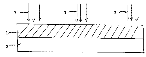
ll FIG. 1 shows the composition of the present
12 invention coated onto a substrate and subjected to
13 imagewise radiation.
14
FIG. 2 shows a substrate supporting an imagewise
16 pattern of permanent resist material.
17
18 FIG. 3 shows the construction of FIG. 2 with
19 conductive material deposited on the substrate.
21 FIG. 4 shows a package of two constructions of
22 FIG. 3 in layered configuration to form a package.
23
24 DETAILED DESCRIPTION OF THE INVENTION
26 It has been discovered that the composition of the
27 present invention, described above, which is curable
28 in response to imagewise radiation, can be coated onto
29 a substrate at thicknesses of at least about 0.0015
inch in a non-brittle, non-distortable layer, thus
31 overcoming one problem of the prior art as described
32 above.
33
34 It has also been discovered that the composition can
be fully cured such that when curing takes place in
36 contact with an epoxy resin-containing substrate the
37 coefficient of thermal expansion of the substrate and
38 the cured composition will be substantially the same
39 in the z axis, thus overcoming the delamination
problem of the prior art described above.
EN985050 6
`` ~2~39~)3
1 It has also been discovered that printed circuit
2 boards comprising the permanent resist composition of
3 the present invention can be fully cured in layered
4 configuration to form a package which resists
delamination.
7 The composition of the present invention requires as
8 component (a), an epoxyfunctional resin which is
9 capable of being partially cured to a resinous state
by the action of a cation-producing photoinitiator.
11 Curing is by a ring opening addition reaction of epoxy
12 moieties which is initiated by cations produced when
13 the photoinitiator is struck by activating radiation.
14 Such reactions are already well known in the resin
technologY-
16
17 Any useful such epoxyfunctional resin may be employed
18 in the present invention. However, in order to
19 function satisfactorily, the resin should have at
least two epoxy groups, and preferably more.
21
22 Good results have been obtained using an
23 octafunctional epoxidized novalac as (a), and such a
24 resin is preferred. The octafunctional epoxidized
novalac is commercially available from Celanese Resins
26 under the tradename SU-8. It will be readily apparent
27 to one of ordinary skill in the resin technology that
28 other such multifunctional epoxy containing resins
29 will be useful in the present invention. Such other
useful resins are within the intended scope of the
31 appended claims.
32
33 Component (a) should be present in an amount of at
34 least about 65 wt. ~ resin solids. The solvent in
which (a) is provided, such as a ketone, is not taken
36 into account when determining the concentration of
37 (a). Concentrations of (a) of less than about 65 wt.
38 %~ when coated on substrates, form coatings which are
39 too soft to be useful. It is preferred that (a) be
present in an amount of from about 78 wt. % resin
* Trademark
EN985050 7
A."
.
~891~3
t solids to about 83 wt. % resin solids. Concentrations
2 of (a) of less than about 78 wt. % begin to form
3 coatings which, when cured, are softer than is
4 preferred, Concentrations of (a) greater than about
83 wt. % have been found to result in cured coatings
6 which are undesirably brittle,
8 Component (b) may be any reactive diluent which is
9 effective as a plasticiser for (a). Reactive diluent,
~ as used herein, is understood to mean a diluent which
'1 will react or crosslink with (a) during curing.
12 Suitabls materials are, for example cycloalaphatic
13 epoxides, although other suitable reactive dilueIlts
14 will readily come to mind to those of ordinary skill
in resin technologies. Such other materials are
16 within the intended scope of the appended claims.
17
18 Good results have been obtained using cycloalaphatic
19 epoxides such as 3,4 epoxycyclohexylmethyl-3,4
epoxycyclohexyl carboxylate and
21 7-oxabicyclo(4.1.0)heptane-3-carboxylicacid,
22 7-oxabicyclo(4.1.0)hept-3-ylmethyleaster. Such
23 materials are commercially available from Ciba Geigy
24 under the tradename CY 179 and from Union Carbide
under the tradename ER 4221.
26
27 Component (b) should be present in a concentration
28 which will constitute from about lO to about 35 wt. %
29 of the resin solids in the composition. It has been
found from experimentation that if less than about 10
31 wt. % of (b) is present the resulting cured
32 composition will be undesirably brittle and that if
33 more than about 35 wt. % is present the resulting
34 cured composition will be undesirably soft.
36 ~ preferred range of (b) is from about 12 to about 17
37 wt. % of the resin solids, depending on the relative
38 softness or brittleness which is desired in the final
39 composition.
ENg85050 8
39~333
1 Component (c) may be any photoinitiator which produces
2 cations acids upon exposure to radiation. The cations
must be produced in amounts sufficient to cause curing
4 Of (a).
6 One group of cationic photoinitiators which are useful
7 in the present invention as component (c) are
8 triarylsulphonium salts. The use of such salts as
9 photoinitiators is known from, for example, U.S.
Patent 4,245,029, issued January 13, 1981, to
11 crivello.
12
13 One suitahle such pho~;oinitiator is a product
14 available from General Electric Company under the
tradename UVE 1014, which comprises a mixture of
16 triarylsulphonium hexafluoro antimonate and thio
17 phenoxy triaryl sulphonium hexafluoro antimonate in a
18 propylene carbonate solvent. It will be readily
19 apparent to those of ordinary skill in the resin
curing technology that other such cationic
21 photoinitiators will be useful in the present
22 invention and are within the intended scope of the
23 appended claims.
24
Component (c) should be present in the composition of
26 the present invention in an amount of from about 2 to
27 about 6 parts (not counting the solvent) per 100 parts
28 Of resin. It has been found from experimentation that
29 concentrations of (c) less than about 2 parts per 100
parts of resin will result in a composition which
31 takes undesirably long to cure upon exposure to
32 radiation.
33
34 It has been observed that concentrations of (c)
greater than about 6 parts per 100 parts resin results
36 in a composition which is not developable ~y
37 chlorinated solvents. When the composition of the
38 present invention is to be used as a photoresist in
39 the manufacture of printed circuit boards it is
important that portions of the composition which are
EN985050 9
~2~39~3
1 not struck by radiation be dissolvable in chlorinated
2 solvents in order to develop the pattern of the cured,
3 radiation struck portions.
Optionally, the composition of the present invention
6 may include an indicator (d) to help determine which
7 portions of the composition, have been struck by
8 radiation. Any useful such indicator which will
9 crosslink with (a) during curing can be incorporated.
One suitable indicator which has been used is
11 epoxidized trishydroxyphenylmethane, which is
12 commercially available from Dow Chemical under the
13 tradename XD 7342. It will be readily apparent to
14 those of ordinary skill in the resin curing technology
that any such indicator may be used and that all
16 useful such indicators are intended to be within the
17 scope of the appended claims.
18
19 Component (d), may be present in amounts of from 0 to
about 5 wt. ~ of resin solids. The
21 trishydroxyphenylmethane indicator described above
22 changes color when it has been struck by radiation of
23 the wavelength which will cause the composition to
24 cure. Thus, technicians working with the composition
can tell which portions of the composition should be
26 cured. It has been observed that amounts of (d)
27 greater than about 5 wt. ~ cause the cured image to
28 lose resolution and increase the photoexposure time
29 undesirablY
31 A second optional component (e) is a surfactant
32 coating aid. The purpose of the coating aid is to
33 produce an even thickness of film across a surface and
34 to prevent defects in the an end product, such as a
printed circuit board which might be caused by
36 non-wetting of the surface- Any useful such coating
37 aid my be employed- One suitable coating aid is a
38 non-ionic surfactant (a fluorinated hydrocarbon)
39 available from the 3M Company under the tradename FC
430. It will be readily apparent to those of ordinary
* Trademark
EN985050 10
-
1 skill in the coating technolo~y that any suitable such
2 coating aid may be used and will be within the
3 intended scope of the appended claims.
Component (e) may be present in amounts up to about
6 0.5 parts per 100 parts resin. It has been observed -
7 that higher concentrations of the surfactant coating
8 aids results in a coated composition which is
9 undesirably slippery.
11 ~ photosensitizer (f) is also an optional component.
12 Any photosensitizer whlch is useful to cause the
13 photoinitiator to absorb more light is suitable. Good
14 results have been obtained using anthracene, perylene
and mixtures thereof, although other useful
16 photocatalysts may come to mind to those of ordinary
17 skill in the resin curing technology.
18
19 The first step in making the composition of the
present invention is the pre-dissolving of component
21 (a) in a suitable solvent. Any solvent which will
22 dissolve any of (a) which is not partially crosslinked
23 can be used. Useful solvents have been found to be
24 methyl isobutyl ketone, methyl ethyl ketone and
mixtures thereof, although other suitable solvents
26 will readily come to mind to those of ordinary skill
27 in resin technologies. The amount of solvent used
28 should be at least enough to dissolve the desired
29 amount of non-partially crosslinked component (a)
31 It is important to the eventual use of the composition
32 as a photoresist in the manufacture of printed circuit
33 boards that the second step of filtering any partially
34 cro~sslinked (a) from the solute be accomplished. If
this step is not accomplished, portions of the
36 unexposed composition will not be soluble in some
37 chlorinated solvents, and the photoresist material
38 will not be as easily developable.
39
EN985050 11
3'33~03
1 Filtering through a 10 micron porous membrane filter
2 has been found to be adequate for the preparation of a
3 composition which will be useful as a photoresist.
After filtering, from about 10 to about 35 wt. ~ resin
6 solids of ~b) and from about 2 to about 6 parts per
7 100 parts resin of (c) are added with stirring. The
sequence of addition is not critical, and any method
9 of stirring can be used.
~1 As an o~tional step, additional solvent may be added
12 in order to adjust the viscosity of the composition.
13 The composition of the present invention may have any
14 Yiscosity; however, when it is intended for eventual
use as a photoresist in the manufacture of printed
16 circuit boards, it is desirable that the composition
17 ha~e a viscoslty of from about 600 to about 2,000
18 centipoise. Although any suitable solvent may be used
~9 for adjusting the viscosity, it is preferable to use a
solvent which is at least similar to the one used to
21 sOlu~ilize (a3
22
23 A photocatylist (f) may be added as an optional
24 component when (b) and (c) are added. As described
a~ove, the photocatylist can be added in amounts up to
26 about 1 wt. ~ of the resin solids
27
28 Optional components (d) and (e) may also be added to
29 the composition with components (b) and (c). The
addition of optional component (d) has been observed
31 to increase the required stirring time of the
32 Composition
33
34 As has been indicated above, the composition of the
present invention is useful as a permanent photoresist
36 on a printed circuit board. In such use composition 1
37 is coated on substrate 2 in FIG. 1. Best results are
38 o~tained when the substrate is a partially cured epoxy
3g resin-containing material such as epoxy resin coated
glass cloth, commonly ~nown as pre-preg in the printed
EN985050 12
~B9~
1 circuit board technolo~y. The composition, when fully
2 cured, substantially matches the coefficient of
3 thermal expansion of such a substrate, which is also
4 fully cured, in the z axis between about 0 C and 100
C. to minimi~e delamination auring use. As used
6 herein, substantial matching of the coefficient of
7 thermal expansion of the epoxy resin-containing
8 substrate and the composition of the present invention
9 means that in the z axis the relative difference
between the expansion of the composition and the
ll substrate over 100 C is less than about 300 micro
12 inches per inch per C.
13
14 The process of using the composition as a permanent
photoresist begins with the step of coating the
16 composition onto such a suitable substrate. The method
17 of coating is not critical and may be by any suitable
18 technique, many of which are known to those of
19 ordinary skill in the coating technology. However, it
is an important advantage of the composition of this
21 invention that it can ~e coated to thicknesses of
22 0.0015 inch and greater. Coatings of such thicknesses
23 are important in the manufacture of printed circuit
24 boards having permanent resist designs. The discovery
of a material which can be coated to such thicknesses
26 overcomes a serious problem of the prior art in the
27 industrialization of the permanent resist technology,
28 as discussed above.
29
For example, the compo~ition may be placed directly on
31 a substrate by a wiping or doctoring technique or by
32 the use of a coating nozzle. However, a more
33 preferred method is to first coat the composition onto
34 a carrier medium, such as Mylar film, and then to
remove solvent by heating or heating in the presence
36 of vacuum until a coating of the desired thickness has
37 been achieved on the carrier medium. An advantage of
38 this preferred method of coating is that the layer of
39 composition on the carrier medium can then be stored
until it is needed for use on a substrate. The
EN985050 13
~9~
1 rheology of the composition on the carrier medium,
2 after some of the solvent has been dried off is such
3 that the carrier mediurn can be rolled for convenient
4 storage. The non-brittle, non-distortable nature of a
layer of the present composition is important in
6 enabling the use of a carrier layer. The parallel
7 plate T of the composition should be between 25 C
8 and 40 C in order for the carrier layer method of
9 coating to work well. In this preferred method,
component (d) has been found useful in helping achieve
11 the T range mentioned above.
12
13 In this preferred method of coating the composition on
14 the substrate, the composition is transferred from the
carrier medium to the substrate by the use of a heated
16 nip roller arrangement or by the use of a heated
17 vacuum laminator; Both such techniques are well known
18 in the coating technology. After lamination of the
19 coating to the substrate, the carrier medium is
stripped away, although stripping does not have to
21 take place at once. The coated substrate can be
22 stored with the carrier medium still covering the
23 coating, if desired.
24
After the carrier medlum is removed, or alternatively
26 after doctor blade coating, the coating on the
27 substrate is exposed to an imagewise pattern of
28 radiation 3 to which it is responsive. The
29 composition described above is responsive to
ultraviolet radiation having a wavelength of less than
31 about 500nm in an amount sufficient to cause the
32 release of Lewis or Bronstead acids from component
33 (c). It has been observed that good results are
34 obtaine~ when the radiation provides at least about
200 milli Joules of energy to the coating.
36
37 If optional component (d) is present in the
38 composi'ion, it will change color in the
39 radiation-struck areas so that a technician can
inspect the pattern of exposure. In the manufacture
EN985050 14
~L~339~3
I of printed circuit bo~rds, the exposure is typically a
2 negative image of the desired conductive circuit
3 patter~. A colored pattern in the composition, when
4 it is used as a p~otoresist as described above, will
indicate at least partial crosslinking in the colored
6 areaS~
8 The exposed co~ting is subsequently developed by
9 exposure to a suitable solvent. A suitable solvent is
one which will solubil~ze non-crosslinked or
17 non-partially crosslinked com~onent la), but which is
12 incapable of dissolving crosslinked or partially
13 crosslin~ed component (a~. The most typical solvents
14 for use in developing photoresists after exposure are
chlorinated solvents, such as 1,1,1-trichloroethane.
l~ The particular solvent used is not critical to the
17 inve~tion. Other useful solvents will come to mind to
18 those of ordinary skill in the printed circuit board
19 manufacture *echnology, and such so~vents are within
the intended scope of the appended claims.
21
22 The development of the exposed composition will leave
23 an imagewise coating o~ partially crosslinked
24 composition on the surface of the substrate. After
development the cure of such an imagewise coating 4 in
26 FIG. 2 is advanced in order to further harden it and
27 to enhance its subsequent use as a resist in metal
28 plating baths. Advancing of the cure of the imagewise
29 resist pattern is accomplished by applying either heat
or light energy. At least about 2 Joules of light
31 energy to which the composition is responsive has been
32 found to be sufficient for this step. Alternatively,
33 heating the substrate and imagewise coating to at
34 least about 100 C for at least about 10 minutes has
been found to provide sufficient energy to advance the
36 cure of the imagewisc resist coatins.
37
38 A conductive materia~ ~ in FI~. 3 is then deposited on
39 substrate ~ in the areas not masked by the imagewise
photoresist coating 4. Deposition of conductive
EN985050 15
l~B~3
1 material 5, which is normally copper, is usually
2 accomplished by use of an electroless metal plating
3 bath, which may be followed by use of an electorlytic
4 metal plating bath. By operation OI the baths, the
use of which are well ~nown in the printed circuit
6 board manufacturing technology, a conductive metal is
7 deposited on the substrate in the areas not protected
8 by the imagewise photoresist pattern so that a pattern
9 of conductive material is deposited on the substrate
in a positive image of a desired printed circuit.
11
1~ It is sometimes desirable that the resist material
13 then be removed from the printed circuit board to
14 leave the conductive pattern on the substrate.
lS However, in other applications, it is desirable for
16 the resist to remain on the printed circuit board. In
17 such uses, the photoresist material is known as
18 permanent resist and such printed circuit boards are
19 known as permanent resist printed circuit boards.
21 When permanent resist is desired, the imagewise
22 composition may be further cured after the step of
23 depositing the conductive material. Further curing is
24 normally done by heating because of the impractability
of supplying sufficient energy as actinic radiation.
26 Good results have been obtained in the present
27 invention by heating the printed circuit board to at
28 least about 175 C for at least about an hour.
29
It is an important advantage of the composition and
31 method of the present invention that, after such
32 further curing, the composition will have a
33 coefficient of thermal expansion in the z axis which
34 is substantially the same as that of epoxy resin-
coated glass cloth which is normally used as a
36 substrate for printed circuit boards. This advantage
37 overcomes serious problems of delamination of
38 permanent resists, as is described above.
39
EN985050 16
1~39~3~3
1 A printed circuit board manufactured by the process
2 described above and using the composition o~ the
3 present invention is intended to be within the scope
4 of the present invention. Such a circuit board may be
of the permanen~ resist design, and, as such, will
6 have the advantage of a reduced tendency to delaminzie
7 because of the substantial similarity of the
8 coefficient of thermal expansion in the z axis of an
9 epoxy resin-containing substrate and the resist
material-
11
12 A package 6 of FIG. 4 of two or more permanent resist
13 printed circuit board constructions 7 and 8 may be
14 made by further curing them together under pressure,
sometimes with an enclosing layer 9. Enclosing layer
16 9 should preferably be of partially cured epoxy resin
17 containing material so that it will more readily match
18 the curing characteristics of the other components of
19 package 6, although any useful material can be
employed. Further curing of package 6 should be done
21 under a pressure of from about 200 to about 500 psi
22 and preferably at about 300 psi. It should be
23 understood that packages of more than two layers of
24 constructions such as 7 and 8 are contemplated.25
26 The invention is illuminated and illustrated in its
27 various aspects by the following examples, which are
28 not intended to be limiting.
29
Exam ~ 1
31
32 Eighty-eight g. of SU-8, which is an octafunctional
33 epoxidized novalac available from Celanese Resins, was
34 mixed with 100 g. methylethyl ketone and filtered
using 10 micron filter paper before 12 g. of CY 179, a
36 cycloalaphatic epoxide available from Ciba Geigy, was
37 added with stirring. 4.0 g. of W E 1014, a
38 triarylsulphonium salt (50% solution) available from
39 General Electric, was added in yellow light.
EN985050 17
' - .
1?~1~9~3~3
1 The resulting composition was coated onto a partially
2 cured epoxy resin coated glass cloth substrate using a
3 doctor blade and checked for thickness at various
4 locations using a micrometer. Average thickness was
about 0.0018 inch with a var`iance of plus or minus
6 0.0003 inch. Parallel plate rheology was used to
7 determine that the T of the coated composition was 40
8 - 43 C (+/- 3 C).
Imagewise exposure of the coating was made using an
11 Oriel ~60 UV generator and a ~touffer resolution
12 guide, after which the coating was dPveloped with
13 1,1,1-trichloromethane to reveal a crosslinked pattern
14 of resist corresponding to the UV radiation struck
areas. Cure of the resist pattern was advanced by
16 baking in an oven at 100 C. for 10 minutes.
17
18 The resist imaged substrate was immersed in a Shipley
19 electroless plating bath until a conductive layer was
built up on the portions not protected by the
21 substrate. The resist was observed to remain intact.
22 The construction was further cured in an oven at 175
23 C. for one hour before the resist was tested on a
24 Perkin Elmer thermomechanical analyzer (TMA) to ~
determine change in the z axis during cycling between
26 0 and 100 C~ Test results indicated less that 100
27 microinches/inch/C. change. Multiple cyclings over a
28 period of time failed to cause delamination.
29
Exam~le 2
31
32 The procedure of Example 1 was repeated using 80 wt.
33 resin solids SU-8 and 20 wt. % resin solids CY 179 to
34 form a composition which was suitable for coating on a
substrate with a doctor blade, but which had too low a
36 T (about 20 C.) to use in the carrier layer coating
37 technique. Once coated, the material functioned
38 substantially as in Example 1.
39
EN985050 18
.. , ~ . ~ , '
.
1289~3
1 ExamPle 3
-
3 The procedure of ~xample 1 was repeated using 88 wt.
4 SU-8 and 12 wt. % CY 179 to form a composition which
could be coated onto a subst~ate using a doctor blade
6 but which was too brittle ~Tg 45 C.) to be used in
7 the above described carrier layer coating technique.
~ Once coated by the doctor blade technique, however,
9 the composition functioned substantially as in Example
10 1.
1~
12 ~Yample 4
13
14 The procedure of Example 1 was followed using 65 wt. %
resin solids SU-8 and 35 wt. % resin solids CY 179 to
16 achie~e a composition having a Tg of 20 C. and not
17 being useful in the carrier layer coating method.
18 ~owever, after coating on the substrate with a doctor
19 blade, the material functioned substantially as in
Example 1.
21
22 Ex2mple _
23
24 The procedure of Example 1 was followed using 85 wt. %
resin solids SU-8 and 15 wt. % resin solids CY 179.
26 The resulting material had a good hardness, but was
27 found to distort substantially and was not useful in
28 the carrier layer transfer method. The composition
29 functioned substantially as the composition of Example
1 after coating on a substrate with a doctor blade.
31
32 Example 6
-
33
34 In this comparative example, 70 wt. ~ resin solids
SU-8 was used with 10 wt. % resin solids XD7342, an
36 epoxydi~ed trishydroxyphenylmethane available from Dow
37 Chemical Co., and 15 wt. % resin solids CY 179 was
38 used in the procedure of Example 1. The resulting
39 composition, which had a Tg ~elow 2~ C was not
4~
EN985050 19
-, : ' -
89~3~3
1 soluble in chlorinated solvents and could not be
2 developed~
4 Example 7
6 The procedure of Example 1 was followed using 80 wt.
7 resin solids SU-8, 5 wt. ~ resin solids XD7342 and 15
8 wt. % resin solids CY 179. The composition had a Tg
9 of 35 C. and was capable of being coated onto a Mylar
film using a doctor blade, dried to remove solvents
11 and then coated onto a substrate using a heated nip
12 roller. The compositi~n performed substantially the
13 same as did the composition of Example 1.
14
1~ Exam~le 8
16
17 The procedure of Example 1 was followed except that
18 the optional components listed below were added in the
19 amounts shown to produce the results shown:
21 a3 fluorinated hydrocarbon.
22 0.5 parts/100 parts resin solids.
23 smoother coating achieved.
24
b) fluorinated hydrocarbon.
26 1 parts/100 parts resin solids (comparative
27 example).
28 smooth coating, but oily resin surface.
2g
c) perylene.
31 0.5 parts/100 parts resin solids.
32 75~i less UV radiation required for imagewise
33 exposure.
34
d~ anthracene.
36 1 part/100 parts resin solids.
37 34% less W radiation required for imagewise
38 exposure.
39
i
EN985050 20
1 Exam~le 9
3 The procedure of Example 1 was followed except that
4 the resin/solvent solution was not filtered in this
comparative ex2mple. Upon development, it was
6 observed that undeveloped deposits of partiall~
7 crosslinked material remained in the non radiated
8 areas.
ExamPle 10
11
12 The procedure of Example 1 was followed except that
13 before further curing, two such constructions were
14 layered together and enclosed on the side having the
exposed patterns of circuitry with a partially cured
16 epoxy resin containiny substrate material to form a
17 package. Further curing of the package was then
18 accomplished at 175 C. for one hour while the package
19 was subjected to a pressure of about 300 psi.
21 The procedure was repeated at 150, 200, 500 and 700
22 psi. No delamination and acceptable TMA results
23 (below 300 microinches/in/ C.) were noted for samples
24 further cured at 200 psi and 500 psi. At 700 psi
image distortion was noted and at 150 psi insufficient
26 adhesion between layers was noted.
27
28 The present invention has been disclosed in the above
29 teachings and in the accompanying drawings with
sufficient clarity and conciseness to enable one
31 skilled in the art to rnake and to use the invention,
32 to ~now the best mode Eor carrying out the invention
33 and to distinguish it from other inventions and from
34 what is old. Many variations and obvious adaptations
of the invention will readily come to mind and these
36 are intended to be contained within the scope of the
37 invention as claimed below.
38
39
EN985050 21
. . . _ ~i
, ,