Note: Descriptions are shown in the official language in which they were submitted.
~2~3
RIDE-T~RO~G~ ENERGY BOOST CIRCUI~
Field of the Invention
The invention is related to the field of supplying power to
a computer. More specifically, the invention is relatPd to a
device and a method which allows a computer to ride through
variations in the power supply voltage without immediately
causing initiation of a shut down procedure of the computer.
I
Back~round of the Invention
~'
Computer users normally depend upon a local electric utility
company to provide energy that is within a specified voltage
range. When the voltage deviates from this range, even
briefly, many computers follow an orderly shut down
procedure. Shutting down results in lost work time for the
operator.
~k-
129~1L3
Devices are known which monitor the power supplied to the
computer and initiate a shut down procPdure when the supply
voltage reaches a certain value, the AC low voltage. The
monitor outputs an AC low signal to the omputer when the AC
low voltage i5 reached. Once this AC low signal is asserted
by the monitor, the shut down procedure is hegun, and the
known devices cause the computer to stop processing and to
perform housekeeping functions which prevent a signi~icant
loss o~ information~
The va~t majority of voltage supply problems are of short
duration, on the order of 100-500 msec. By providing a
device which allows the computer to ride through a short
duration voltage supply problem, the initiation of the shut
down procedure would be avoided in most instances. However,
when the problem persists beyond the short duration, the
shut down procedure should be initiated.
Summary_of the Invention
It is therefore an object of the invention to provide a
method and apparatus which allow a computer to ride through
short duration variations in a power supply voltage.
This and other objects are achieved according to the
invention by a device which delays initiation of a shut down
procedure in a computer, the device comprising an
interrupter for receiving and interrupting an asserted shut
down signal. The interrupter outputs an interrupt signal
when the shut down signal has bsen asserted. A gate trigger
is coupled to the interrupter and triggers an energy booster
to ra~se the power supplied to the computer when the gate
trigger receives the interrupt signal from the interrupter.
A means for monitoring the amount of energy remaining in the
~ ,
~29~)0~L3
-- 3
energy booster is coupled to the energy booster and outputs
a depletion signal when the amount of energy in the energ~
booster is below a reference value. An output stage is
coupled to the interrupter and the means for monitoring and
receives as inputs the interrupt signal and the depletion
signal. The output stage outputs a re-asserted shut down
signal when both the interrupt signal and the depletion
signal are present at the inputs of the output stage.
The above and other objects are also achieved according to
the invention by a method for causing a computer to ride
through a variation in power supplied to the computer, where
the variation is indicated by an asserted shut down signal.
The method comprises the steps of: interrupting the asserted
shut down signal; controlling an energy booster upon
assertion of the shut down signal to boost the power
supplied to the computer; and outputting to the computer a
re-asserted shut down signal to allow initiation of a shut
down of the computer when the energy of the energy booster
is below a reference value and the shut down signal is
asserted.
The device and method according to the present invention
provide the advantage of avoiding the shutting down of a
computer when the variation in the power supply voltage is
of short duration, while still allowing an orderly shut down
procedure to occur if the variation is of longer duration.
Brief Description of the Drawin~s
Figure 1 shows a block diagram of the power input stages of
a computer according to the prior art.
~290~
Figure la is a graph of the voltage across an input
capacitor plotted against the time a~ter the beginning of a
variation in the power supply voltage.
Figure 2 shows a block diagram of ~he power input stages of
a computer according to the present invention.
Figure 2a is a graph of the voltage across an input
capacitor plotted against the time after the ~eginning of a
variation in the power supply voltage.
Figure 3 is a schematic diagram of the ride through circuit
shown in block form in Figure 2 constructed according to an
embodiment of the present invention.
Detailed DescriPtion
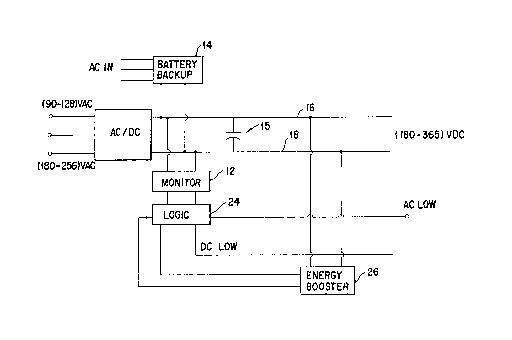
Figure 1 shows a prior art arrangement of power input stages
for a computer. An AC/DC converter 10 converts the utility
voltage to a DC bulk voltage. This DC bulk voltage is
supplied to DC/DC converters, not shown, which power the
computer over lines 16 and 18.
A monitor 12 monitors the DC bulk voltage and outputs two
status signals to the computer shut down logic (not shown)
of the computer. An AC low signal is output over line 20 and
a DC low signal is output over line 22. The AC low signal
in~orms the computer shut down logic ~hat there is just
enough energy left to perform the housekeeping functions
required to prevent a signi~icant loss of information. The
computer stops operating after the AC low signal is
l?9~
, .
asserted. The DC low signal, which is always preceded by the
AC low signal during a power down sequence, in~orms the
computer that one or more DC/DC converters outputs are out
of regulation. The computer is typically down within
microseconds after the assertion of the DC low signal. The
time between the assertion of the AC low signal and the DC
low signal is known as the hold up time, shown graphically
in Figure la (t2-t1), and can be extended by hold-up time
extenders. The time (t1-to) is the ride through o~ a prior
art arrangement operating at a nominally specified utility
power source input. At the minimally specified utility power
source input, this prior art arrangement provides no ride
through.
The battery backup 14 of Figure 1 charges the backup
capacitor 15 to provide enough power for the computer to
maintain a specified level of intelligence during a power
failure. However, not every drop in voltage indicates a
power failure, necessitating initiation of a shut down
procedure. By "riding through" these occasional short
duration voltage drops, the use of the computer will not be
disturbedO One approach to avoiding the initiation of a shut
down is the use of a motor generator with a flywheel to
maintain the input voltage. This approach is expensive in
terms of real estate and cost.
The present invention avoids shut down by interrupting an
assertsd AC low signal and hoosting the voltage with the
arrangement shown in Figure 2. The monitor 12 of the prior
art is connected to a ride through logic circuit 24. As will
be explained in more detail below, the rids through logic
circuit 24 interrupts an asserted AC low signal and triggers
an energy booster 26. Energy boosters themselves are well
known.
~Z~
-- 6
The ride through logic circuit 24 causes the voltage Vc to
be raised by the energy booster 26 when the AC low signal is
asserted. This is illustrated in Figure 2a. A long ride
through time is thereby provided, the ride through time
being defined as the time between loss of nominally
specified utility power source input ~o the computer and the
time at which the voltage Vc has decreased to the AC low
signal voltage (t3 - to) At the minimum specified power
source input, the present invention provides a ride through
time of (t3-tl).
Hopefully, during this ride through time, the voltage supply
has returned to normal, obviating the need for initiation of
a shut down. If at t3 the voltage supply has not returned to
normal and Vc has decreased to the AC low voltage, then shut
down is initiated by the shut down logic, which receives a
re-asserted AC low signal from the ride through logic
circuit 24 on line 28.
An embodiment of the ride through logic circuit 24 according
to the invention is shown in Figure 3, connected to the
energy booster 26. The ma~or components of the logic circuit
24 are an interrupter 30, a gate trigger 32, a comparator 34
and an o-ltput stage 36.
The interrupter 30 receives as an input ~he AC low signal
from the monitor 12. Although other logic can be used, the
embodiment illustrated in Figure 3 comprises a NAND gate 38,
which has as its inputs the AC low signal from monitor 12
and a high signal from a secondary bias source. The primary
bias source is a voltage source referenced to the utility
power source input, whereas the secondary bias source is a
voltage source that is isolated from the primary bias source
-- 7
,, .~
in order to maintain a required safety integrity. The output
of gate 38 will always be low until the AC low signal is
asser~ed (becomes low). The gate 38 will then output a high
signal on line 40 to bsth the gate trigger 32 and the output
stage 36.
The gate trigger 32 receives the high signal on line 40
through resistor 42, which is connected to the gate of
transistor 44. The drain of transistor 44 is connected to a
resistor 46 and a capacitor 48 which are in parallel. The
resistor 46 and capacitor ~8 are each connected to a
transformer 50, the output of which is connected to the
energy booster 26. The transformer provides the required
isolation between the primary and secondary bias sources to
maintain safety integrity for the gate trigger 32 and thus
can be considered an isolating transformer. When a high
signal is on line 40 (the AC low signal is asserted), the
transistor 44 turns on, causing the gate trigger 32 to
trigger the energy booster 26 so that it can raise Vc across
capacitor 15.
The comparator 34 includes an operational amplifier (op amp)
52 which receives at its negative input a reference voltage
established by a zener diode 54 and a shunt resistor 56. The
op amp 52 is powered by the primary bias supply voltage on
line 58. The value of the amount of energy remaining in the
energy booster 26 is input to the comparator 34 at resistor
60, which together with resistor 62~ forms a voltage
divider. The op amp 52 receives at its positive input the
value from the voltage divider, which is proportional to the
value received from the energy booster 26. The op amp 52
outputs a low signal whenever the signal at its positive
input is less than at its negative input. In other words,
1~9~
the op amp 52 will output a low signal when the energy
remaining in the energy booster 26 falls below a refer~nce
value.
The output of op amp 52 is connected to a resistor 64, which
is connected to the input of optical isolator 68. When the
input voltage to the optical isolator is high, a low will be
present at line 70, which is connected between the collector
of optical isolator 68 and the output stage 36. When the
input of optical isolator 68 is low, a high will be present
on line 70. Again, the optical isolator 68 provides the
required isolation to maintain safety integrity for the
comparator 34. In summary, the output of op amp 52 goes low
when the energy remaining in the energy booster 26 falls
below a reference value. This causes the voltage at the
input of optical isolator 68 to go low, which causes a high
signal to be present on line 70.
The output stage 36 is a NAND gate 36 in the illustrated
embodiment. The two inputs for the NAND gate 36 are from the
output of NAND gate 38 and from the comparator 34 (on line
70)~ A low signal will be output from the NAND gate 36 only
when both inputs are high. The low signal is received by a
shut down circuit.
The operation of the ride through logic circuit 24 when an
AC low signal is asserted is as follows. The interxupter 30
receives the asserted AC low signal and prevents it from
immediately reaching the shut down circuit. Upon receipt of
the asserted AC low signal, the output of gate 38 goes high,
which causes gate trigger 32 to trigger the energy booster
26~ The voltage across the capacitor 15 ~Vc) is raised by
the energy from the energy booster 26. The amount of energy
~ ~ - 9
remaining in the energy booster 26 is monitored by the
comparator 34. While there is sufficient energy in the
energy booster 26, the comparator 34 outputs a low signal to
the output stage 36, which therefore does not send the
asserted AC low signal. It is only when the energy in the
energy booster 26 has been depleted below a reference value
that the comparator 34 outputs a high signal to output stage
36. If both the AC low signal is asserted on line 40 and the
energy from the energy booster 26 falls below the reference
value, then the output stage 36 outputs an asserted AC low
signal to the shut down circuit to cause an orderly shut
down of the computer. However, if the power supply voltage
has been restored before the energy from the energy booster
26 has fallen below the reference value, then the comparator
34 does not output a high signal to the output stage 36 so
that the output of gate 36 will remain high, and the shut
down procedure will not be initiated by the computer. Thus,
short duration drops in the power supply to the computer can
be tolerated without immediate initiation of shut down
procedures.