Note: Descriptions are shown in the official language in which they were submitted.
~2903~ RD-17,30/
INTEGRATED CURRENT SENSOR CONFIGURATIONS
FOR AC MOTOR DRIVES
The present invention relates in general to a current-
controlled AC motor drive and more specifically to an AC
motor drive using integrated current sensors built into the
inverter switches.
Background of the Invention
High-quality torque regulation for polyphase AC motors
depends upon accurate control of instantaneous current in
each of the motor phase windings. Such control requires
that instantaneous phase current levels be accurately
10 sensed. Present current-controlled AC drives use discrete -
current sensors in series with the motor phase windings to
sense these phase current levels. One prior art technique
of sensing current flow through such phase winding involves
sensing the voltage drop developed across a resistor that is
serially connected to the winding. Since the possible
current range is large, the sensing resistor must have a
relatively high power rating, which increases its cost.
Alternatively, the current sensors may constitute high-
quality Hall-effect transducers which are also relatively
expensive. All these current sensors must be galvanically
isolated from each other, as well as from the control logic,
and must reject significant common-mode signals associated
with the inverter switching in order to maintain integrity
of the current data. While Hall-effect current sensors can
meet these isolation requirements, they are temperature
sensitive, bulky and fragile, and their output signals are
subject to ofset and drift. High-quality Hall-effect
devices with improved performance characteristics are
available, but at very high cost.
~P
~.29~3`~
RD-17,307
In addition to the above disadvantages, the volume and
isolation requirements for discrete current sensors limit
the possible reduction in size and weight of AC drives to be
obtained through their use, even though the physical size of
power semiconductors used in inverters continues to shrink.
A power semiconductor device, such as an insulated gate
bipolar transistor (IGBT) having a main current section and
a current sensing section that emulates or follows the
current in the main current section, is disclosed in
W~lden and Wil~i in C~nadian Patent Number
1,219,382 which issued March~17, 1987 and
patent has been assigned to the
assignee of the present application. Although some IGBT
switches having integrated current sensors have been
lS fabricated into some AC drives, they function in those
circuits solely to provide overcurrent threshold detection.
As such, they do not provide the complete current
information necessary for closed-loop current regulation.
Objects of the Invention
It is a primary object of the invention to provide a
new and improved current sensor configuration for an AC
motor drive which is not subject to the foregoing
disadvantages.
It is an additional object of the present invention to
provide a new and improved current sensor for an AC motor
drive which makes it possible to achieve current control
without employing discrete current sensors in the indivi~ual
motor phase windings.
It is another object of the present invention to
provide a new and improved inverter which eliminates the
volume and weight penalties imposed by conventional discrete
current sensors.
~l2903~[)
RD-17,307
It is a further object of the prese.nt invention to
provide a new and improved inverter which can be constructed
simply and economically.
Summary of the Invention
In accordance with the principles of the present
invention, an AC polyphase motor drive includes a current-
controlled inverter having current sensing sections
integrated in the inverter semiconductor switches and
diodes. The current sensing sections are formed with the
switch or diode in the same semiconductor fabrication
process, and produce output current signals which are
proportional to the main current in the switch or diode.
Means are provided for converting the signal current from
each current sensor into an output voltage proportional to
the main current in the semiconductor devices.
The above objects and other objects of the present
invention together with the features and advantages thereof
will become apparent from the following detailed
specification with reference to the accompanying drawings in
which applicable reference numerals have been carried
forward.
Brief DescriPtion o the Drawings
Figure 1 is a schematic diagram of a prior art AC motor
drive including discrete current sensors in series with the
motor phase windings;
Figures 2A and 2B illustrate symbols used in subsequent
figures to represent an insulated gate bipolar transistor
having an integrated current sensor and a diode having an
integrated current sensor, respectively;
Figure 3A is a schematic diagram of a basic building
block or a three-phase, full-wave bridge inverter in an AC
~9~3~ RD-17,307
motor drive, employing one device of the type shown in
Figure 2A and one of the type shown in Figure 2B;
Figure 3fi is a schematic diagram illustrating the
series connection of two of the basic building blocks shown
in Figure 3A;
Figure 4 is a schematic diagram of a-preferred
embodiment o~ the present invention, wherein an AC motor
drive includes a three phase full-wave bridge inverter;
Figures 5A - 5D are schematic diagrams of different
types o~ circuits for converting the current from each
current sensor into an output voltage;
Figure 6 is a schematic diagram of a three-phase
full-wave bridge inverter in accordance with another
embodiment of the present invention;
Figure 7 is a schematic diagram of a switched reluc-
tance motor drive inverter in accordance with a further
embodiment of the present invention; and
Figure 8 is a schematic diagram of a basic building
block for a three-phase full-wave bridge inverter in an AC
motor drive, employing a p-channel IGBT with an integrated
current sensor and a diode with an integrated current sensor
referred to the cathode terminal.
Detailed Description of the Invention
With reference to the drawings, Figure 1 illustrates a
prior art three-phase AC motor drive for supplying stator
current to an induction or synchronous motor 10, only the
stator windings of which are represented. These windings
comprise phase windings 40, 48 and 50. The basic elements
of the motor drive include a DC power source (not shown), a
three-phase full-wave bridge inverter 12, and a current
controller 14.
Inverter 12 includes a positive DC input bus 16, a
negative DC input bus 18, and three substantially identical
phase-legs 20, 22 and 24. Each phase-leg supplies an AC
12~39~)
RD-17,307
output current to a different phase, respectively, of
motor 10. Phase-leg 20 includes an AC output terminal 26,
an insulated ~ate bipolar transistor ~IGBT) 28 and a fly~ack
diode 30 connected in parallel between positive DC bus 16
ard AC terminal 26, and an insulated gate bipolar
transistor 32 and flyback diode 34 connected in parallel
between negative DC bus 18 and AC terminal 26. IGBT 28 has
its collector connected to positive DC bus 16 and its
emitter connected to AC terminal 26, while flyback diode 30
has its cathode connected to positive DC bus 16 and its
anode connected to AC terminal 26. IGBT 32 has its
co]lector connected to AC terminal 26 and its emitter
connected to negative DC bus 18, while flyback diode 34 has
its cathode connected to AC terminal 26 and its anode
connected to negative DC bus 18. The gate terminals of
IGBTs 28 and 32 are connected to current controller 14
through conductors 36 and 38, respectively. Conductor 42
passes current between AC terminal 26 and phase windinc 40
of motor 10. Similarly, phase-legs 22 and 24 provide
current to phase windings 48 and 50 of motor 10 through
conductors 44 and 46, respectively.
In operation, a DC voltage is applied across DC input
buses 16 and 18. Current controller 14 operates IGBTs 28
and 32 in accordance with a current command siar.zl IA to
produce an AC current at output terminal 26. IGBTs 28
and 3 are operated so that no more than one of the two
IGBTs is gated on at any instant of time. When IGBT 28 is
gated on via control line 36, load current flows either
through IGBT 28 or diode 30, depending on the direction of
current in the inductive motor phase winding 40. Similarly,
a gating signal applied to IGBT 32 via control line 38
causes current to flow either through IGBT 32 or diode 34.
Thus an AC current is produced at output terminal 26 by
alternately applying gating signals to IGBTs 28 and 32.
The actual current in conductor 42 and phase winding 40
is sensed by a discrete current sensor 52, such as a
903~
RD-17,307
Hall-effect current transducer, and a signal proportional to
the actual current is generated and fed back to current
controller 14 via feedback conductor 58. Current
transrormers cannot be used as the current sensors since
current transformers are insensitive to any DC component in
the measured phase current. The current controller includes
means known in the art for comparing the feedback signal
generated by current sensor 52 to the current command signal
for phase-leg 20 and modifying the gating of IGBTs 2~ and 32
to bring the actual current in phase winding 40 into
agreement with the commanded AC current waveform. Current
controller 14 may be one of the types discussed by D.M. Brod
and D.W. Novotny in "Current Control of VSI-PMW Inverters",
IE~E Transaction on IndustrY A2~1ications, Vol. IA-21, pp.
562-570, May/June 1985.
Similarly, the IGBTs of phase-legs 22 and 24 are oper-
ated by current controller 14 in accordance with current
command signals IB and IC to produce selected AC current
waveforms in phase windings 48 and 50, respectively.
Discrete current sensors 54 and 56 generate respective
feedback signals for phase-legs 22 and 24.
The present invention eliminates the discrete current
sensors 52, 54 and 56 shown in Figure 1 by using current
sensors integrated into the power semiconductors. An
n-channel ir.sulated gate bipolar transistor having an
integrated current sensor is shown in Figure 2A. Within the
IGBT device, but not schematically shown, is a main current-
carrying section and a current sensing section, both sec-
tions being formed onto one semiconductor wafer. The
external connections of the IGBT device include a collec-
tor 64, a control gate 66 and an emitter 68, all of which
connect internally to the main current-carrying section, and
a current sensing terminal 70 which is connected internally
to the current-carrying section of the device. The device
is constructed such that, during operation, the current
sensing section and terminal 70 produce a sensor current
~29~39~ RD-17,307
that is proportional to the current in the main section. As
shown in Figure 2A, the sensor current flowing out of
terminal 70 is Io~Nl, where Io is the IGBT emitter current
flowing in terminal 68 and Nl is the ratio between the
emitter current and the sensing section current. The
ratio N1 is set by the physical design of the IGBT. Details
of the construction and operation of the IGBT device are
shown and described in the aforementioned Walden and Wildi
Canadian Patent Number 1,219,3~2.
Figure 2B shows a diode having an integrated current
sensor. The diode also includes, in one semiconductor
device, a main current-carrying section and a current
sensing section. The anode 72 and cathode 74 connect
internally with the main current-carrying section of the
device and terminal 76 connects internally to the current-
sensing section. During operation, the current sensing
section and terminal 76 produce a sensor current
proportional to current in the main current-carrying section
of the diode. As shown in Figure 2B, the sensor current
flowing into terminal 76 is Io/N2, where Io is the anode
current in terminal 72 and N2 is the ratio between the anode
current and the sensing section current. The ratio N2 is
set by the design of the diode. A diode of this type is
described in the aforementioned Canadian Patent
Number 1;219,382.
Referring again to Figure 1, the basic building block
for the three-phase inverter is the parallel combination of
an IGBT and a flyback diode, such as IGBT 2~ and diode 30.
The complete inverter is comprised of six of these
IGBT-diode combinations as shown in Figure 1. A key element
in the present invention, as shown in Figure 3A, comprises a
parallel combination of IGBT 51 and flyback diode 53 in
which both devices contain integral current sensors.
Provided that the IGBT and the diode are designed to have
the same ratio N between their individual sensing section
currents and the current in their main sections, the two
~29~39~
RD-17,307
sensor terminals can be directly connected at terminal S7.
This direct connection is possible since the current sensor
sections in the IGBT and the diode are referred to the ~ame
reference node, terminal 63. With these connections, the
combined sensor current flowing out of (or into) terminal 57
is It/N, where It is the total current in the IGBT-diode
combination, defined to be positive when current flows out
of terminal 63. It should be noted that the current flowing
into terminal 61 is It x (N+l)/N which is almost identical
to It provided that N is large. Typical values for N are
over 1000, so that the current in terminal 61 can be
considered equal to the terminal 63 current with an error no
larger than 0.1 percent.
Two of the IGBT-diode combinations including the
integral current sensors can be connected in series, as
shown in Figure 3B, to form an inverter phase leg
configuration. IGBT 69 has its collector connected to
positive DC bus 77 and its emitter connected to the AC
output terminal 79. Flyback diode 71 has its cathode
connected to positive DC bus 77 and its anode connected to
AC output terminal 79. IGBT 73 has its collector connected
to AC output terminal 79 and its emitter connected to
negative DC bus 81. Flyback diode 75 has its cathode
connected to AC output terminal 79 and its anode connected
25 to negative DC bus 81. IGBTs 69 and 73 are controlled by
conventional logic circuitry (not shown) which applies
voltages to gate terminals 65 and 67. This logic circuitry
insures that IGBTs 69 and 73 are never turned on at the same
time, avoiding any short circuit across the DC source
terminals 77 and 81.
Current I3 flowing out of (or into) terminal 79, shown
in Figure 3B, must be measured to regulate current flowing
to the motor. Figure 3B also indicates that current I1
flows out of the upper IGBT-diode combination 83, while
35 current I2 10ws into the lower IGBT-diode combination 85.
Kirchoff's current law demands that the load current I3
~ 2 9 0~ ~0 RD-17,307
equal the sum of I1 + t-I2), so that current I3 can be
reconstructed if currents Il and I2 are known separately.
Since both the upper and lower IG8T-diode combinations 83
and 85, respectively, in Figure 3B include integral current
sensors, measurements of currents I1 and I2 are available at
terminals 87 and 89, respectively, to reconstruct the
desired load current I3 measurement.
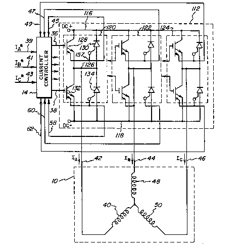
Figure 4 illustrates a preferred embodiment of a
three-phase AC motor drive in accordance with the present
invention. Inverter 112 includes three substantially
identical phase-legs 120, 122 and 124, each connected
between positive DC input bus 116 and negative DC input
bus 118. Each of the three phase-legs is configured as
shown in Eigure 3B. For example, phase-leg 120, which
supplies current to phase winding 40 of motor 10, includes
an AC output terminal 126, insulated gate bipolar
transistors 128 and 132 having integrated current sensors,
and flyback diodes 130 and 134 having integrated current
sensors.
Current controller 14 alternately operates IGBTs 128
and 132 of phase-leg 120 via gate terminals 36 and 38,
respectively, in order to produce a desired AC current
waveform in phase winding 40. Measurements of current in
the upper IGBT-diode pair 128 and 130, respectively, are fed
back to the current controller 14 via conduc-tor 45, and
measurements of current in the lower IGBT-diode pair 132
and 134, respectively, are Fed back by a separate
conductor 58. Current controller lg combines these two
separate measurements to pro~ide a measurement of the total
phase-leg output current iA delivered to the motor over
conductor 42. The current controller regulates the
switching operation of IGBTs 128 and 132 to bring the actual
phase-leg output current IA in conductor 42 into agreement
with the commanded current waveform IA delivered to the
current controller on conductor 39. Phase-legs 122 and 124
are substantially identical to phase-leg 120 in construction
390
RD-17,307
and similar in operation except that the current
waveforms I~ and IC flowing in conductors 4~ and 46,
respectively, are 120 and 240, respectively, out of phase
with the waveform of current IA of phase-leg 120.
Reerring bac~ to Figure 3A, the sensor output signal
at terminal 57 is a scaled current It/N which is
proportional to the total phase-leg current It flowing out
of the IGBT-diode combination through terminal 63. It is
typically con~Tenient for the current controller to convert
this small sensor current into a voltage representing the
measured current It which is then used by the current
controller to regulate the amplitude of current It.
Figure 5A illustrates a circuit for converting the
current derived from an IGBT to a voltage signal. The
emitter of IGfiT 78 is connected to the positive input
terminal of an operational amplifier 80, while the current
sensing terminal of IGBT 78 is connected to the negative
input terminal of operational amplifier or op-amp 80. A
feedback resistor 82 is conne-ted between the op-amp
negative input terminal and its output terminal. The
amplitude of the output voltage referenced to the IGBT 78
source, assuming ideal op-amp characteristics, will be
-(Io x R~N), where:
Io = current in the main current section of
IGBT 78;
R = ohmic value of resistor 82; and
N = ratio between the main-section current and
the current-sensing-section current
in IGBT 78.
Figure 5B shows a circuit for providing a voltage
signal proportional to the sensor current combination
derived from an IGBT and a flyback diode connected in
parallel, the IGBT and diode having the same current sensing
ratio, N. The emitter of IGBT 84 and the anode of diode 86
--10--
9~)39~
RD-17,307
are connected to the positive input terminal of op-amp 88
and the current sensing section terminals of both devices
are connected to the negative input terminal of the op-amp.
A feedback resistor 90 is connected between the negative
input terminal and the output terminal of op-amp 88. The
output voltage signal from the op-amp, re~erenced to the
IGBT 84 source, is -(Io x R/N~ assuming ideal op~amp
characteristics, where:
Io = total current in the main current-carrying
sections of IGBT 84 and diode 86;
R = ohmic value of resistor 90; and
N = current sensing ratio discussed above with
reference to Figure 5A.
Figure 5C shows another circuit for generating a
voltage signal proportional to the sensor current
combination derived from an IGBT and a flyback diode
connected in parallel, the IG3T and diode having different
current sensing ratios. The emitter of IGBT 92 and the
anode of diode 94 are connected to the positive input
terminals of a set of op-amps 96, 99 and 105. The cur-er.t
sensing terminal of IGBT 92 is connected to the negative
input terminal of op-amp 99, while the current sensing
terminal of diode 94 is connected to the negative input
terminal of op-amp 96. The output terminals of op-amps 96
and 99 are connected to resistors 102 and 103, respectively.
Resistors 102 and 103 are both further connected to the
negative input terminal of op-amp 105. The op-amps may be
considered to have ideal characteristics.
Feedback resistors 97, 100 and 106 are arranged between
the negative input terminals and output terminals of
op-amps 96, 99 and 105, respectively. R2 is selected to be
equal to R1 x N2/N1, where Rl and R2 are the ohmic values of
resistors 97 and 100, respectively, and Nl and N2 are the
current sensing ratios of diode 94 and IGBT 92,
respectively. The ohmic value of each of resistors 102
and 103 is chosen equal to R3. Thus, the output voltage
~9~3~3~
RD-17,307
signal from op-amp 105 will be (Io x R1 x R4)/(Nl x R3),
where:
Io = total current in th~ main current-carrying
section of IGBT 92 and diode 94;
Rl = ohmic value of resistor 94;
R3 = ohmic value of resistors 102 and 103;
R4 = ohmic value of resistor 106; and
N1 = current sensing ratio for diode 9~.
Figure SD shows a signal conditioning circuit which
converts the integrated current sensor signals from the
upper and lower IGBT-diode combinations 83 and 85,
respectively, shown in Figure 3B, into a single output
voltage proportional to the phase-leg AC output load
current. The emitte~-anode terminal 79 from the upper
IGBT-diode combination 83, shown in Figure 33, is connected
in the circuit of Figure 5D to the positive input
terminal 179 of op-amp 113, and the current sensing section
terminal 87 from the upper IGBT-diode pair 83 of Figure 3B
is connected in the circuit of Figure 5D to the negative
input terminal 187 of the op-amp. The emitter-anode
terminal 81 from the lower IGBT-diode combination 85, shown
in Figure 3B, is connected in the circuit of Figure 5D to
the positive input terminal 181 of op-amp 117, and the
current sensing section terminal ~9 from the lower
IGBT-diode pair 85 of Figure 3B is connected in the circuit
of Figure 5D to the negative input terminal 189 of the
op-amp. In Figure 3B, the current sensor output 87 signal
from the upper IGBT-diode pair 83 is Il~N and the sensor
output 89 signal from the lower IGBT-diode pair 85 is I2/N.
30 These signals are indicated at input terminals 187 and 189
in Figure 5D.
Op-amps 113 and 117 in Figure 5D are each connected in
the same circuit configuration as shown in Figure 5B so that
the output voltage from op-amp 113 is -(I1 x Rl/N) and the
output voltage from op-amp 117 is -(I2 x Rl~N).
Amplifier 123 is an isolation amplifier with a gain of 1
-12-
~L29~
RD-17,307
whose output voltage is galvanically isolated from the input
terminals 119 and 139 in order to provide level-shifting.
This element is needed since ~he integrated current sensors
in the upper and lower IGfiT-diode pairs are referred to
different voltage levels. Again referring back to
Figure 3B, the emitter-anode connection 81 for the lower
IGBT-diode pair 85 is connected to the negative DC source
voltage, whereas the voltage at the emitter-anode
connection 79 for the upper IGBT-diode pair 83 switches
between the positive and negative DC source voltages 77
and 81 depending on the IGBT conduction states. As a result
of this voltage difference, it is necessary to use some
means such as an isolation amplifier to provide
level-shifting so that t~e current sensor signals from the
1~ upper and lower IGBT-diode pairs can be electrically
combined. The output stage of isolation amplifier 123 of
Figure 5D is referred to the negative DC source voltage by
means of conductor 141.
The output voltage from isolation amplifier 123 is
-(Il x Rl/N) since the gain of this amplifier is unity.
This output voltage is applied to the negative input
terminal of op-amp 133 through a resistor 127 of ohmic
value R2, and the output voltage of op-amp 117 is applied to
the positive input of op-amp 133 through a resistor 129 with
the same ohmic value R2. Op-amp 133 serves as a difference
amplifier in this circuit. Accordingly, resistor 135 with
value R3 is connected between the positive input terminal of
op-amp 133 and reference voltage terminal 181. Feedback
resistor 131 connected between the output terminal 137 of
op-amp 133 and the negative input terminal has the same
ohmic value R3. As a result, the output voltage from this
circuit at terminal 137 is (Il - I2) x Rl x R3 / (R2 x N)
where N is the current sensing ratio for all of the IGBT and
diode sensor elements, and where the op-amps are considered
to have ideal characteristics. As described earlier with
reference to Fi~ure 3B, (Il - I2) is equal to the phase-leg
-13-
~29039~
RD-17,307
AC output current I3, so that the output voltaye at
terminal 137 developed in Figure 5D is proportional to the
load current as desired. This load current measurement can
then be used as feedback information to replace a discrete
current sensor (such as sensor 52, 54 or 56) in the prior
art scheme illustrated in Figure 1.
Alternative embodiments of the invention are
illustrated in Figures 6 and 7, wherein different
constructions of inverter 112 of Figure 4 are shown. In the
embodiments shown in Figures 6 and 7, as is also the case
with the preferred embodiment shown in Figure 4, current
controller la is connected to receive feedback information
from a first group of semiconductor devices consisting of
those IGBTs and diodes which have integrated current
sensors. Current controller 14 uses this current feedback
information in combination with current command signals to
develop output gating commands which are delivered to all of
the IGBTs in the inver~er to control their conduction
states.
Figure 6 shows a three-phase full-wave bridge inverter
which is configured so that only the devices connected to
the negative DC input bus contain current sensing sections.
This configuration eliminates signal conditioning
difficulties associated with extracting current data from
the switches connected to the positive DC bus as shown in
Figure 4. These difficulties are due to common-mode voltage
components which must be eliminated from the feedback signal
and which arise because the emitters of the upper phase-leg
IGBTs, i.e. the IGBTs connected to the positive DC input
hus, are being s~itched between the positive and neyative DC
bus voltages at high fre~uencies. This embodiment
eliminates the need for special level-shifting elements such
as the isolation amplifier 123 in Figure 5D.
In the circuit of ~igure 6, the inverter comprises a
35 positive DC input bus 216, a negative DC input bus 218, and
three phase-legs 220, 222 and 224. Phase-leg 220 includes
-14-
~2 ~ 90 ~D-17,307
an AC output terminal 226, an IGBT 228 and a flyback
diode 230 connected between positive DC bus 216 and AC
terminal 226, and an IGBT 232 and a flyhack diode 234
connected between negative DC ~us 218 and AC terminal 226.
IGfiT 232 and diode 234 contain current sensing sections.
The current sensing terminals of IGBT 232 and diode 234
provide sensor current feedback signals iA at ~erminal 258
from phase-ley 220 to the current controller, as shown in
Eigure 4. In this configuration, however, feedback data are
generated only when IGBT 23~ and diode 234 are carrying
current. Phase-legs 222 and 224 are identically configured
and operate in a similar manner. A control algorithm for
regulating the output current when only partial feedback
information is available is described in Jahns
Canadian Application Serial No. 586,015 filed December
15, 1988 and assigned to the assignee o~ the present
invention.
In accordance with a ~urther embodiment of the
i~vention, a variable frequency three-phase
switched-reluctance motor drive inverter is shown in
Fiqure 7. The inverter comprises a positive DC input
bus 416, a negative DC input bus 418, and three
phase-legs 420, 422 and 424 Phase-leg 420 includes a pair
of output terminals 426 and 427 which are connected to motor
phase winding 440. An IGBT 428 has its collector connected
to positive DC bus 416 and its emitter connected to output
terminal 426, and a 1yback diode 430 has its cathode
connected to positive DC bus 416 and its anode connected to
output terminal 427. An IGBT 432 has its collector
connected to output terminal 427 and its emitter connectet
to negative DC bus 418, and a flyback diode 434 has its
cathode connected to output terminal 426 and its anode
connected to negative DC bus 418.
In operation, a voltage potential is applied across DC
input buses 416 and 418. The current controller (not shown)
operates IGBTs 428 and 432 in accordance with a current
_~,5_
~.~9039C)
RD-17,307
command signal to provide current to motor phase
winding 440. The current in winding 4ao, which is connected
between output terminals 426 and 427, passes
unidlrectionally between DC input buses 416 and 418.
However, the magnitude of this current is made to vary by
operation of IGBTs 428 and 432. The operation of IGBTs 428
and 432 differs from operation of their counterparts in the
synchxonous motor or induction motor drives described
previously, in that IGBTs 428 and 432 are both switched into
conducting (or non-conducting) states concurrently during a
portion of their respective operating cycles.
Only the IGBTs and diodes connected to the negative DC
bus 418 incorporate current sensors therein. For exa~ple,
only IGBT 432 and diode 434 in phase-leg 420 include
integrated current sensors providing sensor output current
signals on conductors 452 and 454, respectively. As
mentioned above, the inverter for the switched reluctance
motor differs from the previously-described AC motor
inverters in that both IGBTs in a phase-leg for the switched
reluctance motor can be turned on at the same time. As a
result, the inverter can be operated so that complete
information about the motor load current flowing in
winding 4ao is always available, even though the upper
IGBT 428 and diode 430 do not include integrated current
sensors. Signal conditioning circuits to convert the sensor
output currents from the lower phase-leg IGBTs and diodes
into voltages can be accomplished using simple op-amp
circuits as described previously in conjunction with
Figure 5. Since all of the lower phase-leg current sensors
are referred to the same reference voltage on bus 418, no
special level-shifting elements such as isolation amplifiers
are necessary to reconstruct the motor current measurements.
Although the invention described herein has thus far
been described in terms of n-channel power devices, the
techniques apply equivalently to p-channel devices. For
example, the upper IG~T 128-diode 130 combination in
~X~3~ RD-17,307
.
Figure 4, employing an n-channel IGBT, can be replaced by
the corresponding p-channel IGBT-diode combination as shown
in Figure ~. IGBT 551 is a p-channel device with an
integrated current sensor, and diode 553 is designed to
include a current sensing section referred to the cathode
terminal. As a result, the current sensors in IGBT 551 and
diode 553 are both referred to emitter-cathode connection
terminal 561. Assuming that the IG~T and diode are designed
to have the same current sensor ratio N, the sensor current
flowing into terminal 556 is a scaled version It/N of the
total current It flowing into (or out of) the
emitter-cathode terminal 561. Signal conditioning circuits
such as shown in Figure 53 to convert the sensor current
into sensor voltages ~re easily adapted to the p-channel
IGBT-diode combination of Figure 8 by using the
emitter-cathode terminal 561 as the circuit reference node
instead of the emitter~anode connection in the n-channel
version.
The preceding discussion and accompanying drawings
describe a new and improved current sensor configuration for
an AC motor drive which makes it possible to achieve current
control without requiring discrete current sensors in the
individual motor phase windings. The circuitry can be
constructed simply and economically and permits a reduction
in the size of AC motor drives through the elimination of
discrete current sensors and their associated volume and
weight penalties.
From the foregoing specification, it will be clear to
those skilled in the art that the invention is not limited
to the specific embodiments described and illustrated and
that numerous modifications and changes are possible without
departing from the scope of the present invention. For
example, although the preceding discussion has dealt with AC
drives for three-phase motors, the invention is equall~
applicable to AC supplies for any polyphase load. Also,
while the drive inverters described and shown employ
-17-
, -
~90390
RD-17,307
insulated gate transistors and flyback diodes, the main
switching devices may employ any of a variety of MOS
~metal-oxide-semiconductor)-gated devices or even bipolar
transistors rather than insulated gate bipolar transistors,
with integral current sensing portions where appropriate.
Other variations, changes, substitutions and
equivalents will be readily apparent to those skilled in the
art without departing from the spirit and scope of the
invention. Accordingly, it is intended that the invention
to be secured by Letters Patent be limited only by the scope
of the appended claims.
-18-