Note: Descriptions are shown in the official language in which they were submitted.
. " lX9046~L
- 1 - 6920~-150
Field of the Invention
The invention relates to apparatus for testing printed
circuit boards.
Ba`ck'grou'nd'of't'he'Inve'ntion
Printed circuit boards (PCB' S) loaded with the compon-
ents they were designed to carry are often tested for electrical
integrity by using spring-loaded test pins that are vertically
supported undernea-th a printed circuit board under test (BUT) in
position to contact the exposed nodes on the bottom surface of
the BUT.
For example, Katz United States Patent No. 4,132,948
discloses mounting test pins in an unloaded PCB having an identi-
cal hole pattern to that of the BUT so that the test pins auto-
matically line up with the nodes being contacted. The test pins
are directly connected to wires that are connected via cable
assemblies to the test circuitry. When the circuit board tester
is to be used to test PCB ' s having a di~erent node pattern, the
test pin support board is replaced w;~th one having test pins
corresponding to the node locations for the new PCB design.
Published European Patent Application No. 0 115 135
discloses a test fixture including a permanent base sheet carrying
a large number of test pins and a lowe~ custom~z~ board that
carries inserts that activate
~Z9(~46~
_ 2
test pins at selected locations to be raised into
activated position to contact nodes of a BUT. When used
with a different BUT, a new customizing board, having
:inserts in the same pattern as that of the nodes of the
new BUT, is installed. Underneath the customizing
board, wire wrap post extensions of the inserts are
wired to terminals at the side of the customizing board,
for connection to test circuitrY-
Published European Patent Application No. 0 050
913 discloses a test fixture including a general purpose
platform that carries test pins in a uniform grid
pattern and a backing plate that carries removable
displacement modules that activate test pins at selected
locations to contact nodes of a sUT. On the other side
of the backing plate are wire wrap posts that are
electrically connected to the test pins through the
modules and are wired to a multiple pin plug at the edge
of the backing plate.
In some prior art test systems channel circuit
boards containing instruments for providing test signals
to the BUT's and receiving resulting outputs were
physically located underneath the test pins to reduce
the distance between the instruments and the BUT to
reduce distortions to test signals and outputs. In such
systems there were a plurality of upwardly directed
channel nodes at connectors at the upper ends of a
plurality of channel boards (also referred to as channel
cards), the channel nodes being electrically connected
by wires to respective test pins carried on a test pin
support board like that shown in Katz U.S. Patent No.
4,132,948. The test pins were wired to upwardly
directed right angle posts on small boards, the lower
plated edges of which were in turn connected to
zero-insertion force edge card connectors mounted on
~291)461
~ 3 ~
r the channel cards. Before making the wire wrap
connection to the right angle posts, the small boards
carrying them were removed and turned upside down so
;that the posts were directed downward, the same
direction as lower extensions of the test pins, to
facilitate wire wrapping, and after wire wrapping, the
small boards were rotated back and mounted in the edge
card connectors with the wires folded over. In these
systems, when a particular automatic tester was used
with different types of BUT's having nodes at different
locations, new test pin support boards were installed.
A particular modeI automatic tester could be provided
with different channel boards having different
instrumentation, depending on the type of BUTs to be
tested, and a user might want to add or modify channel
boards, with the result that there would be different
channel nodes for the same model of tester, and possibly
even the same machine at different times.
In another prior art system, dual-ended test
pins mounted on a probe plate in one pattern were
electrically connected to probes connected to test
circuitry in another pattern below the probe plate by a
translator board between the two carrying upwardly
directed wire wrap posts in position to contact lower
spring-biased contacts of the dual ended test pins,
downward extending wire wrap posts in position to
contact lower test circuitry probes, and wires between
various wire wrap posts.
Summary of the Invention
In one aspect my invention features in general
a printed circuit board tester in which electrical
connection can be desirably made between spring-biased
board under test (BUT) contacts in a first pattern of
~29C~4~
g~ `''l
4 ~
predetermined locations corresponding to the nodes of a
BUT and channel nodes of test circuitry circuit boards
in a region below the test pins in a different pattern
by using a translator board having both tubular housings
carrying the spring-biased suT contacts extending from
its upper surface and lower conductors extending from
its lower surface and aligned with the channel nodes and
translator means electrically connecting the respective
tubular housings to lower conductor members. The use `of
tubular housings for BUT contacts and lower conductors
on a common translator board permits one to make
electrical connection between BUT contacts and channel
nodes in different patterns simply and directly,
facilitating signal integrity in the path from the sUT
nodes to test circuitry on the,channel boards.
In preferred embodiments the lower conductors
are wire wrap posts that extend through holes in a
keeper plate below the test pin support board; and there
is an interface assembly below the keeper plate making
electrical connection to the channel nodes.
In another aspect my invention features
providing a translator board (for making electrical
connection between upper conductors in one pattern and
lower conductor in another) below a universal test pin
support board having test pins in a grid pattern of
possible BUT locations, the translator board carrying
displacement members for actuating selective test pins
corresponding to node locations for the particular BUT.
When used with a different BUT, a new translator board
is used to both actuate only those test pins that
correspond to the positions of the BUT nodes and to make
electrical connection between them and the respective
test circuitry channel nodes.
~L29~)461
~ . ~
5 69204-150
In another aspect my invention features a urinted
circuit board testex in which a universal board having spring
biased interface contacts in a universal grid is used to make
electrical connection between test pins and channel nodes of test
circuitry, the channel nodes being in an application specific
pattern that is a subset of the universal grid. Displacement
members in the same pattern as the channel nodes are used to move
into actuated position only those spring-biased contacts that are
needed to connect to the channel nodes. When the channel nodes
are changed, e.g., when the instrumentation on the channel circuit
boards is changed to chanye instrumentation, a different pattern
of channel nodes can be easily accommodated by simply using
different interface contacts on the universal board.
In accordance with a broad aspect of the invention there
is provided apparatus for testing the electrical inteyrity of a
plurality of printed circuit boards under test (BUT), each said
aUT having a plurality of downwardly directed accessible BUT nodes
at a first pattern of predetermined locations in a first field on
its bottom surface, said apparatus comprislny
support means for removably supporting a said BUT,
test circuitry including a plurality of channel circuitry
printed circuit boards having associated upwardly directed channel
nodes, said upwardly directed channel nodes and said channel
circuitry printed circuit boards being directly below said support
means at a second pattern of predetermined locations in a second
field overlapping said first field, said second pattern not
matching said first pattern of predetermined locations,
~29046~
5a 69204-150
connection means for electrically connecting said
channel nodes to said BUT nodes,
said connection means including spring-biased BUT probe
contacts in a pattern that matches said first pattern so as to be
aligned with and to contact said BUT nodes when said BUT is
mounted on said support means,
said connection means also including a translator board
carrying a plurality of upper conducting members comprising
tubular housings extending from an upper surface of said
translator board, said upper conducting members being electrically
connected to and carrying said BUT probe contacts, said translator
board also carrying a plurality of lower conducting members
extending downwardly from the lower surface of said translator
board, said lower conducting members being mounted in a pattern
that matches that of said channel nodes, said connection means
also including translator means electrically connecting respective
said tubular housings to respective said lower conducting members.
In accordance with another broad aspect of the invention
there is provided apparatus for testing the electrical integrity
of a plurality of printed cir~uit boards under test (BUT), each
said BUT having a plurallty of downwardly dlrected accesslble BUT
nodes at a first pattern of precletermined locatlons in a flrst
field on lts bottom surface, said apparatus comprising~
support means for removably supportlng a said B~T,
test circuitry including a plurality of channel circuitry
printed circuit boards having associated upwardly directed channel
nodes, said upwardly directed channel nodes and said channel
1~9046~
5b 69204--150
circuitry printed circuit boards belng located directly below said
support means at a seaond pattern of predetermined locatlons in a
second field overlapping said first field, said second pattern not
matching said first pattern of predetermined locations,
connection means for electrically connecting said channel
nodes to said BUT nodes,
said connection means including spring-biased BUT probe
contacts in a pattern that matches said first pattern so as to be
aligned with and to contact said BUT nodes when said BUT is
mounted on said support means,
said connection means also including a translator board
carrying a plurality of upper conductiny members extending from
its upper surface and aligned with and electrically connected to
said BUT contacts, said translator board also carrying a
plurality of lower conducting members extending downwardly from
the lower surface of said translator board, said connection means
also including translator means electrically connecting respective
said upper conducting members to respective said lower conductlng
members,
said first pattern of predetermined location.s being a subset
of a universal grid pattern of possible BUT locations, said
connection means comprislng a universal test pin support hoard
located between said translator board and said BUT, sald universal
test pin support board carrying kubular housiny ln said grid
pattern at locations corresponding to posslble locations for said
BUT nodes, said BUT contacts being mounted in said housings and
extending upward from said universal test pin support board, the
5c 6920~ 150
number of said BUT contacts and tubular housings being larger than
the number of said downwardly directed accesslble BUT nodes, each
said housing also carrying a movable actuating BUT portion on the
other side of said universal test pin support board to cause a
said suT conta~t to be moved upward into an actuated position to
contact a said BUT node when said actuating portion has been
pushed upward by a said upper conducting member directly below it,
and to be in a lower, unactuated position when there is no first
conducting member directly below it.
In accordance with another broad aspect of the invention
there is provided apparatus for testing the electrical integrity
of printed circuit boards under test (BUTs), each said BUT having
a plurality of downwardly directed accessable nodes, said
apparatus comprising:
support means for removably supporting a said BUT,
spring-biased BUT contact means supported by extending within
said support means in position to contact said BUT nodes,
test circuitry including a plurality of channel circuitry
printed circuit boards that have associated upwardly directed
channel nodes, said upwardly directed channel nodes and said
channel circuitry prlnted ci.rcuit board belng located dlrectly
below said support means, said channel nodes belng located ln an
applicatlon speclfic pattern,
a universal board below said support means and above said
channel nodes and carrying tubular housiny in a universal grid
pattern o~ possible channel node locations, said application
specific pattern being a particular subset of said universal grid
~L29C)461
Sd 6920~-150
pattern of possible channel node locations, said application
specific pattern being a particular subset of said universal grid
pattern, and
a plurality of electrically conducting displacement members
supported above said channel nodes at locations in a pattern that
matches said application specific pattern, said displacement
members being electrically connected to said test cirGuitr~
through said channel nodes,
each tubular housing carrying an upwardly directed universal
contact extending from the upper surface of the universal board
and having an actuating portion extending from the lower surface
of said board to cause electrical connection to be made between
said BUT contact and channel node when a displacement member is in
line with said universal contact.
Other features and advantages of the invention will be
apparent from the following description of preferred embodiments
thereof and from the claims.
DescriPtion oP the Preferred Embodiments
The drawings will be briefly described first.
Drawi~s
Figure 1 is a diagrammatic vertical sectional view
showing apparatus for testing PC~'s according to the invention.
Figure 2 is a diagrammatic vertical sectional view of a
test pin assembly of the Figure 1 apparatus.
Figure 3 is an end view of a spring of the Figure 2 test
pin.
~2~146~
5e 69204-150
Figure 4 is a side view of a portion of the Elyure 3
spring.
Figure 5 is an elevation o~ a dlsplaeement pin and a low
pin of the Figure 1 apparatus.
. .
~290461
- 6 - 69204-150
Figure 6 is a diagrammatic vertical sectional view of an
alternative test pin assembly according to the invention.
Figure 7 is a diagrammatic vertical sectional view of
another alternative test pin assembly, shown with a modified sup-
por~- structure, according to the invention.
Figure 8 is a diagrammatic vertical sectional view show-
ing an alternative, most-preferred embodiment of apparatus for
testing PCB's according to the invention.
Figure 9, on the second sheet of drawings, is an eleva-
tion (partially in section) of a universal probe used in the
Figure 8 device.
Figure lO, on the second sheet of drawings, is an enlarge-
ment of a portion of Figure 9 with the probels plunger in a
different position.
Structure
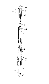
Referring to Figure l~ there is shown apparatus lO for
testing the electrical integrity of a printed circuit board under
test (BUT) 12 loaded with components 14, some of which have leads
which pass through holes in the board and are soldered at nodes 16
to conductive paths printed on the bottom o~ board 12. Some com-
ponents 14 are surface mounted (either on the top or bottom of
board 12) and electrically connected to conductive pads acting as
nodes without solder. Each diferent design or a BUT 12 has a
unique pattern oE nodes 16 associated with it. The nodes of BUT
12 are located on a 0.1" X-Y grid pattern; i.e., they are at
~.290~6~
- 6a - 69204-150
locations in a unique pattern that is a subset of a un:iversal
grid pattern. (The Figure 8 alternative embodimant is used with
BUTs having nodes that are not on an~ grid pattern.)
".,~, .
-` ~Z~3046~
Starting near the top of apparatus 10, it
includes side walls 18 providing overhanging portions 19
against which 10" by 10" diaphragm plate 22 (0.187"
`thick fire resistant glass-filled phenolic board
available under the trade designation FR4, often
referred to as G-10) is biased by springs 20. Diaphragm
plate 22 has 0.07" diameter holes through it spaced on
0.1" centers and rubber sealing ring 23 (1/8" high and
1" wide Neoprene) around the perimeter of plate 22
providing a vacuum seal with overhanging portion 19 and
BUT 12. Two pointed 1/8" thick guidance pins 24 extend
upward through corresponding holes in BUT 12 to properly
align board 12. Also provided at selected locations on
the surface of plate 22 are various rubber support pads
(not shown) which act to seal holes in BUT 12 or support
it to avoid flexing of BUT 12 during evacuation of the
region below it.
Pivotally mounted on side wall 1~ at pivot 26
is universal test pin support board 28 carrying test
pins 30, each of which has a tubular housing 34, an
upwardly directed universal BUT contact 45 and a
downwardly directed actuating plunger 42 (Fig. 2). End
29 of universal board 28 is supported by ledge 31.
Universal board 28 is made of two 1/8" thick
glass-filled phenolic boards (same material as plate 22)
spaced from each other by 3/4" to provide an overall 1"
thickness. Test pins 30 are mounted in holes 32 in
universal board 28 located on 0.1" centers (i.e., in the
universal grid pattern mentioned above) and aligned with
the holes of diaphragrn plate 22.
Referring to Fig. 2, it is seen that each test
pin 30 includes gold-plated nickel-silver tubular
housing 34, which has an outer diameter of 0.054".
Housings 34 are tightly fit in 0.055" inner diameter
. ~, . .
~L29046~L
- test pin sockets 35, which are fixedly mounted in
support board 28 and have shoulders 37 spaced by 3/4" to
provide proper spacing and structural support for
universal board 28. ~ousing 34 is 1.470" long, and has
first crimp 36 located 0.130" from its top, a second
crimp 38 located 0.380" from its bottom and a dimple
(not shown) holding it firmly, though removably, in test
pin socket 35. Contacting plunger 40 and actuating
plunger 42 are slidably carried in housing 34 with
compression spring 44. Plungers 40, 42 are made of heat
treated beryllium copper, gold over nickel plate, have
pointed BUT contact 45 and actuating portion contact 47
for making good electrical contact, bulbous portions 46,
48, respectively, for interfering with crimps 36, 38,
and overhanging shoulders 50, 52, which are larger than
the diameter of housing 34. Spring 49 has an unloaded
length of 0.570", and is music wire wound to 29
oz/inch. Referring to Figs. 3 and 4, it is seen that
the ends 54 of spring 44 have off-center, reduced
diameter portions; this causes spring 44 and bulbous
portions 46, 48 to be transversely biased against the
inner surface of housing 34 only when spring 44 is
compressed, in order to make good electrical contact.
When spring 44 is not compressed, plungers 40, 42 and
spring 44 are freely slidable in housing 34.
Returning to Fig. 1, 3/8" thick, removable
actuating/translator board 56 (made of the same material
as plate 22) carries beryllium copyer displacement
member pins 57, low pins 58 and alignment pins 59 which
are received by bushings 60 carried by sidewalls 24 and
62, supported by housing 92. Each displacement member
pin 57 has a 0.05" diarneter, 1/4" high projection 64
(E'ig. 5) extending above board 56, and each low pin 58
has a 0.05" diameter, 0.08" high projection 65. The
4S~
. -- g
. upper surfaces of projections 64 are concave so as to
guide and restrain pointed ends 47 of test pins 30.
Each pin 57 or 58 has a 0.068" diameter intermediate
:knurled portion 66, which is press Eit into board 56,
and a 0.025 square wire wrap post 68 extending below
board 56.
Supported underneath actuating/translator board
56 are rows of sockets 70, fewer in number than test
pins 30, carried by the upper ends of channel cards 73
(daughter printed circuit boards that are all supported
on their lower ends by a common, horizontal backplane,
not shown), and aligned with and adapted to receive and
make electrical connection with selected posts 68. The
selected posts 68 are either integral with projection 64
of a displacement pin 57 or connected by wires 72 to a
post 68 of a displacement pin 57. Wires 72 are wrapped
around overlapping translator portions that overlap each
other at corresponding positions along vertical axes.
Sockets 70 are electrically connected to the electronic
circuitry on circuit cards 73 and other circuitry of the
tester.
Referring to Fig. 8, there is shown apparatus
110 for testing the electrical integrity of BUT 112
loaded with components 114 and having nodes 116 on the
lower surface that are not at locations of any grid
pattern. Each different design for a BUT 112 has a
unique pattern of nodes 116 associated with it.
Apparatus 110 includes a fixture assembly 118, which is
dedicated to a particular design for a BUT 112, and a
universal interface assembly 120, which can be used with
any fixture 118 and with any pattern of channel nodes
12~, provided by the tops of posts 210 associated with
channel cards 124.
:
',,
~2~
- 10 - l69204-150
Fixture assembly 118 includes sidewalls 126,
having upper overhanging po~tions 12~, against which
translator board 1~0 (0.31" thick G10 material~ is
supported, and lower overhanging portions 131, against
which apertured keeper plate 132 (1/8" thick clear Lexan*
polycarbonate) is supported. Supported near the
periphery of the upper surface of translator board 130
are Neoprene*rubber sealing ring 134 (1/8" high and 1"
wide) and springs 136. Diaphragm plate 138 ~0.187" G10
material) is above sealing ring 134 and springs 136.
Thereabove is Neoprene rubber sealing ring 140 (3/16"
high and 1" wide). Aluminimum sealing ring 192 is
between the peripheries of the lower sur~ace of sealing
ring 140 and the upper surface oE translator board 130.
On top of sealing ring 140 is L-shaped cross section
trim ring 144.
Translator board 130 includes in it upwardly
extending test pins 146A-E and downwardly extending
lower conducting members 148. Test pins 196A-E include
tubular housings 145 (also referred to as upper
conducting members) carrying spring biased ~UT contacts
150 and lower extensions 1~7, including 0.025" squace
wire wrap posts 154A-E therebelow. Lower conductors 14B
also include lower wire wrap posts 156, which overlap
wire wrap portions Oe posts 154A-E and extend through
holes 158 in keeper plate 132. Keeper plate 132 of
fixture 118 sits on an outer Neoprene rubber sealing
ring (not shown) providing a seal between it and
universal interface board 180.
Three wire wrap situations are shown in Fig.
8. In the first example, shown on the left, wire wrap
post 154A of test pin 146A is connected by w;re 160 to
the wire wrap post 156 of adjacent lower conductor 148,
which is aligned with the channel node to which
* Trade-mark
1 `: .
~,,,~ .,
~2~46~
- test pin 146A is to be connected. In the middle
example, wire wrap post 154B of test pin 146B is
connected by wire 161 to wire wrap post 156 of adjacent
:lower conductor 148, and the wire wrap post 154C of test
pin 146C is electrically connected by wire 162 to wire
wrap post extension 164, which is directly below test
pin 146C and is physically connected by insulator sleeve
166 to post 154C. In the example on the right, test pin
146D is electrically connected by wire 167 to wire wrap
post 156 of adjacent lower conductor 148, and test pin
146E is electrially connected by wire 168 to wire wrap
post extension 170, which is directly below test pin
146D and physically connected by insulator sleeve 171 to
post 154D.
Universal interface assembly 120 includes
universal interface board 180 (3/8" thick G10 material),
which is pivotally mounted at an end (by means not
shown) and carries universal probes 181 comprising
tubular housings 182 having universal interface contacts
184 extending upward from them. Tubular housings 182
similarly have downwardly directing actuating plungers
186. Probes 181 are located in two rows per channel
card, 96 probes deep and spaced on 0.1" centers.
Channel cards 124 are spaced by 3/4". Referring to
Figs. 9, 10, contacts 184 are on plunger 188, which
includes lower portion 190 extending from the bottom of
tubular housing 182 and having recess 192 receiving test
probe 194 (075 center line, .160 travel, cup probe).
Plunger 188 is hiased upward by spring 196, bearing
against the lower annular surface of enlarged portion
198 and inner annular surface 200 of housing 182.
Spring 196 has zero preload; at 0.09" deflection there
is a 4 oz. force on contacts 184, 186. O-ring 202 (O.D.
0.075 + 0.002", I.D. 0.0360 + 0.002") provides a vacuum
. ~
. . ,
~I X90~61
- 12 -
seal between the outer surface of plunger 188 (O.D.
0.041 + 0.002") and the inner surface of housing 182
(I.D. 0.070 + 0.002"), and is retained between roll
crimp 204 and crimped end 206. A synthetic lubricant
S applied to O-ring 202 and the just-mentioned surfaces
provides sliding. Interface contacts 184 have
depressions therein for receiving the lower ends 208 of
wire wrap posts 156 and extensions 164, 170. Plungers
186 similarly have depressions receiving the upper ends
of posts 210 (0.025" square section), extending upward
from connectors 212 of channel cards 124. Posts 210 are
supported within U-shaped transverse supports 213,
connected to respective channel cards 124 (by means not
shown).
OPeration
In operation of the Figs. 1-5 apparatus, an
actuating/translator board 56 having displacement pins
57 mounted in locations corresponding to the accessible
nodes 16 of BUT 12 (i.e., their locations are at a
unique pattern that matches that of BUT 12) is mounted
within device 10 by sliding its guide pins 59 in
bushings 60 while universal board 28 is in a raised,
vertical position. Posts 68 are inserted with zero
insertion force into respective sockets 70, which are
then laterally translated (by a mechanism not shown) to
provide good electrical connection. Universal support
board 28 is then rotated to the horizontal position
shown in Fig. 1 such that its end 29 is supported by
ledge 31. As universal board 28 is lowered into
position, the actuating plungers 42 of test pins 30
aligned with displacement pins 57 are pushed upward. As
plunger 42 slides upward inside of housing 34, it pushes
spring 44 upward and contacting plunger 40 and its
universal ~UT contact 45 through a hole in diaphragm
L2904~i~
plate 22 into the raised position, as is shown in Fig.
1. This requires no more force than the weight of the
two plungers and the spring. BUT 12 is then mounted
:into position using guidance pins 24, and it rests on
ring 23 and springs 20. ~ vacuum is then applied to the
region underneath BUT 12, causing ring 23 and springs 20
to be compressed and BUT 12 to be lowered so that nodes
16 contact the corresponding universal BUT contacts that
have been raised, compressing springs 44. Only the
springs of the test pins that have been raised are
compressed, limiting the force that needs to be applied
to make contact.
Universal BUT contact 45 digs into the solder
or contact pad at node 16, making good electrical
contact. The reduced diameter ends 54 of spring 44
cause sideways biasing of bulbous portions 46, 48,
making good electrical contact through test pins 30.
Actuating portion contacts 47 are biased downward by
spring force and similarly make good electrical contact
with projections 64 of displacement pins 57. Electrical
connection to electronic circuitry is made either
directly to a socket 70 under a displacrnent pin 57 or
through a wire 72 to the post of a low pin 58 that is
received by a socket 70.
The electronic circuitry of the tester provides
test signals to BUT 12 and senses the responses. The
short, direct wire wrap connections between overlapping
wire wrap portions promotes signal integrity, something
becoming increasingly more important with higher speed
digital circuits and obtaining precision analog
rrleasurements .
When it is desired to test a different design
for BUT 12, the universal board 28 is pivoted to a
vertical position, and actuating/translator board 56 is
~29~
replaced with a new actuating/translator board 56 having
displacement pins 57 corresponding to the nodes 16 for
the new BUT 12. In this manner different PCB designs
can be accommodated by merely changing
actuating~translator boards 56, and there is no need to
dedicate the relatively expensive test pins 30 in a
particular predetermined pattern. Also, it is much
easier to accommodate changes in the design of BUT 12 by
changing the location of projection pins 58, than it is
to change the locations of test pins and connections to
tester circuitry in the dedicated test pin position
testers.
In operation of the Figs. 8-10 apparatus,
fixture 118 for a particular BUT 112 is mounted on
universal interface board 180, sitting on an outer
sealing ring and registered by guide pins (both not
shown). At this time the upper ends of those interface
contacts 184 that have been raised are slightly below
lower ends 208 of wire wrap posts and extensions, and
the springs that bias interface contacts 184 have zero
force (ignoring the weight of contacts 184) on them, as
they are not preloaded. A vacuum is then applied
between translator board 130 and universal interface
board 180, causing compression of the sealing ring
between keeper plate 132 and board 180, contact of lower
ends 208 with interface contacts 184, and slight
compression of springs 196. At the sarne time, lower
contacts 186 are lowered to contact channel nodes 122,
and the associated springs in probes 194 are also
compressed slightly. Because interface contacts 184 are
not preloaded, and only those contacts that are being
used are compressed, electrical contact is made with
very little force.
12904~.
- 15 -
sUT 112 is then placed on top of the fixture,
and its BUT nodes 116 are slightly spaced frorn BUT
contacts 150. A second vacuum is applied between BUT
;112 and the upper surface of translator board 130, and
this causes compression of rubber rings 134, 140 and
contact between BUT contacts 150 and BUT nodes 116.
BUT contacts 150 of fixture 118 are in a unique
pattern that matches that of the BUT nodes 116 in the
field of possible node positions of BUT 112. There
similarly is a unique pattern for channel nodes 122 in a
corresponding field under BUT 112; the difference in the
positions of respective test pins and respective contact
nodes is accommodated for by wire wrapping using wires
160, 161, 167, and 168. Wire wrap posts 156 of lower
15 conductors 148 and wire wrap post extensions 164, 170
are in the same pattern as channel nodes 122. Signal
integrity is promoted by the short, direct wire wrap
connection between overlapping wire wrap post portions.
For a given model of test apparatus 110,
channel nodes 122 will be in different positions
depending on the instrumentation desired by the
manufacturer, in turn depending on the BUTs to be tested
and the desired tests. In addition, channel cards 124
and their associated channel node positions on a
particular machine could be changed by adding channel
cards or modifying channel cards at some point in the
future. Universal interface assembly 120 would still be
used with any type of channel card arrangement and with
any type of fixture 118 for a BUT 112, thus
standardizing and simplifyin~ the structure of the
machine.
~L~9(~6~
- 16 -
~' Other Embodiments
Other embodiments of the invention are within
the scope of the following claims.
: For example, an alternative test pin design,
test pin 74, is shown in Fig. 6. Its spring 76 has a
2.5 oz preload and a force of S.4 oz at 2/3 travel.
Test pin socket 78, which is still fixedly mounted in
support board 28, has a 0.056" inner diameter,
permitting 0.054" outer diameter housing 80 to slide in
it. In use, displacement pins 57 push housing 80
upward, along with plungers 40, 42 and spring 76.
A further alternative design for supporting
test pihS is shown in Fig. 7. Here, test pin support
board 83 is made of a single l/2" thick support board
(same material as plate 22) that has counter-sunk holes
81 for accommodating heads 82 of standard, single
plunger test pins 84. Pins 84 can slide within holes 85
through board 83. Caps 86 at the lower end of pins 84
prevent the pins from falling out when support board 83
is turned upside down. Insulating honeycomb 90 is used
to electrically isolate test pins 84 and align them with
their respective displacement pins 57. In use, the
entire test pin 84 is moved upward by a displacement pin
57.
Also, although the systems described herein
have BUTS at the top and channel cards at the bottom,
the inventions herein apply to other orientations.