Note: Descriptions are shown in the official language in which they were submitted.
- ~ \
s
- 1 -
HOT ELECTRON TRANSISTOR
Field of the Invention
This application pertains to the field of active semiconductor devices.
In particular, it pertains to transistors in which a substantial fraction of the current
is carried by hoe electrons, including ballistic electrons~
5 Background of the Invention
It has been known for some tirne that a hot electron transistor,
especially a ballistic transistor, could potentially be operated at frequencies in
excess of those achievable with conventional (diffusive) transistors. See, for
instance, T. E. Bell, IEEE Spectrum, February 1986, pp. 36-38. Various types of
10 hot electron transistors (HET) have been proposed. This application is concerned
with one particular class of HETs, namely, compound semiconductor HETs. For a
brief review, see L. F. Eastman, ibid, pp. 42-45.
Essentially all the prior art work on compound semiconductor HETs
has been concerned with GaAs-based devices, and recently ballistic transport has15 indeed been observed in GaAs-based research devices. A. F. J. Levi et al,
Physical Review Letters, Vol. 55(19), pp. 2071-2073; M. EIeiblum et al, PhysicalReview Letters, Vol. S5(20), pp. 2200-2203 and M. I. Nathan et al, IEEE
Spectrum, February 1986, pp. 45-47.
The ballistic transport was observed in devices having geometries that
20 are thought to hold promise for irnplementadon as a practical HET. The first
type, frequently refelred to as a planar doped barrier transistor (PDBT, see forinstance, J. 1~. Hayes et al, Electronic Letters, Vol. 20(21), pp. 851-852) or
"camel" ~ansistor, J. M. Shannon, IEEE Proceedings, Vol. 128(9), pp. 134-140
(1981)) uses theImionic injection and comprises emitter, base, and collector, with
25 an appropriately shaped potential ba~ier between emitter and base, and a second
barrier between base and collector. The second type, which is referred to as a
tunneling hot electron transIer amplifier (THE~TA, see for instance, M. Heiblum,Solid State Electronics, Vol. 24, pp. 343-366) differs from the first type in having
tunnel injection into the base. Both of the above types are unipolar; however,
30 bipolar HETs have also been proposed in GaAs/AI(3aAs.
The flow of electrons from emitter to base is controlled in both types
by varying the emitter/base barrier potential by means of an applied voltage Veb.
Similarly, the flow of electrons from the base to the collector can be controlled by
9~
-2-
means of an externally applied voltage V~ between base and collector. Under normal
operating conditions, Vbc reverse biases the base/collector junction. Electrons injected
from the emitter into the base have energy substantially greater than the therrnal
S energy of the ambient electrons in the base. These "hot" electrons ideally traverse the
base without undergoing significant scattering. If the base/collector barrier is caused
to be lower than the hot electron energy then some of the hot electrons can cross the
barrier, be transmitted through the depletion region of the collector, and enter the sea
of conduction electrons in the collector.
As will be readily lmderstood by those sldlled in the art, various
difficulties have to be overcome before a device of this type can function as a
practical HET. Among these dif~iculties is quantum mechanical reflection of the hot
electrons by the base/collector barrier, and space charge limited current. Probably the
greatest obstacle, however, is the difflculty of achieving substantially complete hot
lS electron transport through the base, and, desirably, also through the depletion region
of the collector.
See, for instance, A.F.J. Levi et al., Applied Phvsics Letters, Vol. 48(23),
pp. 1609-1611(1986) which discloses means for achieving improved HETs. Among
the means are use of a direct bandgap compound semiconductor material in the
20 "transit" region of the HET, with the condition electrons in the transit region material
having relatively small effective mass, advantageously substantially smaller than the
conduction electron effective mass in GaAs. Furthermore, the transit region
comprises a compound semiconductor material in which the total scattering rate of
the hot electrons is relatively small, advantageously substantially less than the
25 scattering rate would be in GaAs of identical ambient electron resistivity. Exemplary
of such materials are InAs, InSb, InGaAs, HgCdTl, and PbSnTe.
However, even though HETs that incorporate the teachings of the '494
patent application can attain perfonnance levels that are substantially better than
those obtainable with a GaAs-based HET of the same geometry, the performance
30 levels are in many cases still inadequate for practical HETs. For instance, prior art
HETs are generally incapable of producing substantial current gain (e.g. ~ ~ 10,where ~ is the common emitter current gain) at room temperature (300 K), and
typically need to be operated at low temperatures (e.g., 77 K).
"'""` ~L,~90a6~
- 3 ~
In view of the operational simplification that results from the
possibility of room temperature operation of a HET, and of the general desirability
of improved chauacteristics such as ,B, means for achieving further improvementsin HET characteristics would be of considerable significance. This application
S discloses such means.
Definitions
Electron transport in a crystal is herein defined to be "ballistic" if, in
addition to its possible interaction with an accelerating electric field, the electron
interacts substantially only with the static part of the lat~ice potential. Electron
10 transport thus may be ballistic even though the electrons undergo some small
angle scattering and/or small energy change.
A conduction electron herein is considered to be a "hot" electron in a
given semiconductor region if its energy E is substantially greater than EF, theFerrni energy in the region. Typically, E > Ef+lOkBT, where kB is the
15 Bolt~ann constant, and T is the absolute temperature of the lattice.
A "hot electron" transistor (HET) is a transistor whose operative
characteristics are in substantial part determined by the transport of hot electrons
through the transit region of the transistor, with minimal scattering of the hotelectrons in the transit region.
The "transit region" of a HET herein is that portion of the ~T
through which substantial hot electron transport takes place, or is intended to take
place. For instance, in a PDBT, camel transistor, or THETA device, the transit
region consists of the base and the collector depletion region. In order to haYe the
possibili~ of significant hot electron transport in a HET, the width of the transit
25 region has to be less than the mean-free path of the hot electrons in the material.
The "ambient" charge carriers are those charge carriers (elect;ons or
holes) that are essentially in thermal equilibrium with the lattice. For instance, in
bipolar ~Ts the ambient charge caITiers in the base typically are holes.
Sumrnary of she Invention
In a broad sense, I am herein teaching apprs)aches that can be used to
produce HETs of improved charac~eristics. For instance, the inventive approachescan result in compound semiconductor HETs having substantial current gain (e.g.,,B > 10) at room temperature. Such transistors can bç used in a variety of
applications and likely will make possible apparatus operating at higher
35 frequencies than is possible with prior art transistors.
``` ~290~3~iS
- 4 -
HETs of interest herein generally have geome1ries similar to those of
prior art HETs. They comprise an electron emission region (the first region), anelectron collection region (the third region), and a second region that is
intermediate the first and third regions and fo~ms interfaces therewith. The first
5 region comprises an emitter layer, and the second region comprises a base layer,
with typically the emitter layer contacting the base layer and forming the
emitter/base interface therewith. The base layer is typically also in contact with
third region material and forms the base/collector interface therewith. The first,
second and third regions each generally consist of one or more layers of
10 compound semiconductor rnaterial, with the composition of the base layer
diffeAng at least from that of the emitter layer. In some cases (e.g., in some
bipolar HETs) the second region material may be basically the same as the third
region material, with the second and third region materials containing differentdopants and/or differing in dopant concentration.
1~ HETs of interest herein also comprise means for making electrical
contact with the first, second and third regions, respectively, and means for
injecting hot electrons from the first into the second region. At least a substantial
fraction (advantageously > 90%) of the injected hot electrons transit the secondregion without substantial energy loss and cross the base/collector interface. The
20 injected hot electrons have average energy Ei, and their average velocity may be
different in the differen~ regions. Fur~ermore, with the injected hot electrons is
associated a crystal momentum vector ki having a component ki 1 perpendicular
to, and a component ki 2 parallel to, the ernitter/base interface.
I have ~iscovered that the characteristics of a HET can strongly
25 depend on the materials used to cons~uct the device. For instance, the emitter
layer and the base layer advantageously consist of materials which have band
structures such that the hot electrons injected into the base layer have trajectories
that are substantially normal to the emitter/base interface, typically such thatki 2/ki 1 is less than about 0.2. This condition helps to ensure that a relatively
30 large fracdon of the injected electrons can transit the base layer without
undergoing substantial scattering. Exemplarily, this conditdon can typically be met
if the emitter layer comprises an indirect, wide bandgap material such as AlSbAs,
the base layer comprises material (exemplarily InAs) that has a conducdon band
centered on the r-point in k-space (the terminology used to describe the band
35 structure is conventional and well known to those skilled in the art), and the hot
-` ~29~8~5
- 5 -
electrons are injected into these direct r-states.
Furtherrnore, the materials are most advantageously chosen such that
the hot electron velocity component no~rnal to the base/collector interface does not
undergo substantial change upon crossing of that interface. This requires that the
S normal component of aEi/ak be substantially continuous (preferably changing byno more than about 20%) across the base/collector interface. In this expression Ei
is the average energy of the hot electrons, k is the electron wave vector, and ~signifies the partial derivative. The condition ensures that quantum mechanical
reflection and resonances due to the presence of the interface are minimized. In10 order for more than about 90% of the hot electrons to be transmitted in the
forward direction through the inter~ace, the velocity component normal to the
interface (for electrons of energy Ei) should typically change by at most about
11% upon crossing of the interface, and in preferred embodiments of the invention
this condition will be met. AlSb and InAs are exemplary ernitter layer and base
15 layer materials that can advantageously be used in a HET according to the
invention.
There are other means that can optionally be employed to improve the
characteristics of a HET. For instance, ensuring quantization of the occupied
ambient conduction electron states in the base layer results in constraints on
2û scattering and thus increases the probability that a hot electron can traverse the
transit region ballistically. Such quantization results if at least one dimension of
the base layer is very small, typically of the order of 10 nm. A very "thin" base
layer that results in ~ormadon of a substantially 2-dimensional electron gas in the
base layer introduces constraints on scattering, but a base layer that is not only
25 thin but also narrow (and thus is substantially l-dimensional) typically constrains
scatteling even furthe~. Quantization of the ambient charge carriers in the baselayer also increases the effective bandgap and thereby reduces the probability of
interband scatteling.
IncoIporation of these and other features (to be discussed below) into
30 a HET can result in a device having substantially improved perforrnance, as
compared to phor art devices. ~n particular, devices according to the invention
can have room temperature ,B > 10 for a bias (Vce) greater than about 1 volt.
More particularly, HETs according to the inven~ion comprise the
previously referred to first, second, and third regions, the second region being35 intermediate the first and third regions, forming interfaces and being epitaxial
9~86~;
- 6 -
therewith. The first, second, and third regions each consist of compound
seni~conductor material, with the composition of the second region material
di~fering at least *om that of the first region material at the first/second region
interface. The HET further comprises means for making electrical contact with
S the first, second, and third regions, respectively, and means adapted for causing
injection of hot electrons of average energy Ei from the first into the second
region, with at least some of the inj~cted electrons crossing the interface between
the second and the third region. Associated with the hot electrons is a wave
vector ki having components ki 1 and ki 2 that are respectively pelpendicular and
10 parallel to the first/second region interface, and a velocity component normal to
the first/second region interface. The first, second, and third region materials are
chosen such that in the second region material there are empty electron states at
energies substantially equal to Ei, such that associated with the empty electronstates is a wave vector component ki 2 that is substantially equal to the
15 corresponding wave vector component of at least some of the electrons of energy
Ei in the first region material, and such that the component of velocity of the hot
electrons normal to the second/third region interface undergoes relatively smallchange upon crossing of the second/third region interface.
Brief Description of the Drawings
FIG. 1 schemadcally depicts a device according to the invention;
FIG. 2 shows schematically some features of the conduction band
structure of a device according to the invention;
FIG. 3 schernatically shows pordons of the energy level diagrams of
three materials use~ul in the practice of the invention; and
FIG. 4 gives room temperature current gain curves measured on an
exemplary device acco~ding to the invendon.
Detailed Descnpdon of Some Preferred Embodiments
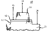
FM. 1 schematically depicts a HET 10 according to the invention,
wherein 11, 12 and 13 arc the first, second, and third regions, respecdvely, and 14,
30 15, and 16 are means for making electrical contact to the first, second, and third
regions, respectively. It will be appreciated that in many cases the first and third
regions can be identified with emitter and collector respectively, and typically each
comprise more than one layer, and that the second region comprises the base
layer. Portion 17 of the third region is a collector depledon region. Exemplarily,
35 11 compIises AlSbo 92Aso 08' 12 consists substandally of InAs, and 17 and 13
~90~3Ç;S
- 7 -
comprise GaSb. Exemplarily, the base layer is about 10 nm thick.
FIG. 2 shows schematically the conduction band of a double
heterojunction HET according to the invention under bias, with numerals 20, 21,
and 22 referring to the first region, the base, and the third region, respectively.
S The arrow indicates the direction of flow of hot electrons, ~eb and ~bC are the
emitter/base and base/collector energy baniers, respectively (associated with the
emitter/base and base/collector interfaces, respectively), Eo is the quantum-
mechanical confinement energy (due to the 2-dimensional nature of the electron
gas in 21), and EF is the Fermi energy in the second region. For the above
10 referred to exemplary combination of materials, (Peb can be about 1.3 eV, and (PbC
about 0.8 eV.
Currendy preferred embodiments use thermionic emission to inject hot
electrons of a~erage energy Ei from the emitter layer into the base layer. Spacecharging effects in the two barriers can be substantially avoided if the barrier15 regions are doped to a dopant density p > j/ev, where e is the electron charge,iis
the current density, and v is the average electron velocity in the respective barrier.
Reverse culrent flow from the base to the emitter layer can be minimized by
choosing ~eb and ~bC to be substantially greater than the ambient therrnal energy
kBT (kB is the Boltzmann constant, and T is the absolute temperature). Typically20 ~PbC > 0.5 e~ for a room temperature HET.
The injection of hot electrons into the base is in general most efficient
if both energy and momentum parallel to the emitterlbase interface are conserved.
Thus the emitter layer and base layer are advantageously chosen such that there
are in the base layer empty states at energy Ei, and that associated with ~hese
25 empty states are wave vectors ki that have components ki 2 that are substantially
equal to ~he corr~sponding wave vector component of the electrons of energy Ei in
the emittel layer.
The above is schematically illus~ated in FIGS. 3a and 3b, which show
relevant portions of the band diagrams of exemplary emitter and base layer
30 materials, respectively. As can be seen from FIG. 3a, electrons of energy close to
Ei have in this em~tter material (exemplarily AlSb) wave vectors close to the X-point in the Brillouin zone and thus, in a (100) oriented device, there are electrons
occupying X-point minima with small ki 2 (ki 2~/a~ and other X-point minima
with large ki 2 (ki 2~~/a~ where a is the lattice constant of the emitter layer
35 material). Similarly, FIG. 3b shows thae electrons of energy close to Ei have in
3.~2~ ;S
- 8 -
this base layer material (exemplarily InAs) wave vectors close to the r-point.
This exemplary combination of emitter layer and base layer materials permits
relatively efficient injecdon of hot electrons (of energy approxirnately equal to Ei)
from the emitter layer into the base layer. In particular, the efficiendy injected
5 electrons are from the X-point minima with small ki 2~ which go into the smallki 2~ r-like states in the base layer material. Electrons from the other X-pointminima cannot be efficiently injected because no empty states with large ki 2 are
available in the base layer mateAal. Thus the injected electrons have only smallvelocity components parallel to the emitter/base interface, resulting in increased
10 probability that the hot electrons can traverse the transit region ballistically~
A practical HET not only requires efficient injecdon of the hot
electrons into the base but also substantially complete transmission of the hot
electrons over the base/collector potendal barrier. The probability that an electron
is reflected at the base/collector interface decreases as the change of electron15 velocity upon entering the collector region decreases. Since the velocity is
propordonal to aE/~k, ~his suggests that advantageously the rnaterials are selected
that ~E/ak Ei 2 ~ aE/~k Ei 3~ wh~re the partial derivatives are to be taken
at the average energy of the hot electrons, and subscripts 2 and 3 refer to the
materials on either side of the base/collector interface.
An apprGximate alternative expression of the velocity matching
condition, derived from effective mass theory and introduced for illustradve
purposes only, is m21m3~ Ei/(Ei-~), where m2 and m3 are the effective
electron masses in the base and collector material, respectively. Thus, by careful
choice of Ei, q~bc. base and collector materials (including the possible use of an
25 appropriately designed superlattice in the collector dçpletion region), quantum
refleceions from ~ can be minimized. Typically, such matching is possible ~or a
relatively small range of electron energies (exemplarily about 0.5 eV). Thus, it is
ad~rantageous to choose the emitter material and ~eb such that the injected
electrons have a relatively small energy spread.
Furthermore, high transmission through the base/collector interface
typically requires that ~e electron wave function in ehe collector be similar incharacter to that in the base (e.g., both be s-like for electrons of energy Ei). For
instance, the choice of InAs as base and GaSb as collector material makes
possible satisfaction of both of the above matching conditions, as is illustrated by
. .. .
~1 ~9l~ 5
FIGS. 3b and 3c, in which the latter shows the relevant portion of the band
diagram of an exemplary collector material (exemplarily GaSb). At energy Ei the
electrons in both the base and the collector rnaterial are near the ~-point in k-
space and thus have s-like wavefiJnctions, and the slope of the conduction bands5 at Ei are similar in the two materials.
There are further means that may optionally be used to improve the
operating characteristics of a HET according to the invention. For instance, I have
found that in a device having dimensions such that the base region comprises
quantized electron states there exist kinematical constraints (due principally to
lO energy and momentum conservation) that reduce the probability of electron-
scattering below that in the bulk. Thus it is advantageous to reduce at least one
dimension of the base region (typically its thickness) such that the ambient charge
carriers in the base behave in the manner of a quasi 2-dimensional charge carrier
gas. Typically, this r~quires that the thickness is less than about 50 nm,
15 preferably less than about 20 nm. Further reduction in the effective
dimensionality of the ambient charge carrier gas can fur~er reduce the scattering -;
probability. For instance, application of a magnetic field normal to the base layer
can result in a reduction of hot electron scattering by a substantial amount,
exemplarily a factor of 2-10. As will be appreciated by those skilled in ~he art,
20 such a magnetic field can impose lateral confinement on the charge carrier motion,
resulting in an effectively 0-dimensional charge carri.er gas. An e~fectively l-dimensional charge ca~ier gas can be produced by means of a thin and narrow
(e.g., < 50 nm) strip of base layer material.
It has also been found that electron scattering probabilities frequendy
25 depend strongly on the final state into which the electron is scattered. For
instance, in InAs scattering of (100)-directed hot electrons into L-minima is
typically less likely than into X-minima. Therefore, the injection energy Ei is
advantageously chosen to be less than the energy associated with the X-minima.
On the other hand, it is not essential that Ei is also less than the energy associated
30 with the L-minima. This discovery obviously results in greater design freedom,
while maintaining low scattering of the hot electrons.
In HETs with two classes of mobile charge carriers (e.g., bipolar
HETs) it is frequently desirable that the effective heavy hole mass mh be much
greater than me, the effective elec~on mass, since this also gives rise to kinematic
35 constraints on scattering. For this effect to be significant, it is typically desirable
~z9o~s
- 10 -
that mhlme>l0 perpendicular to the base/collector inter~ace. Exemplarily, this
condition can be met by use of a strained base layer.
It will be obvious to those slcilled in the art that all three regions of an
inventive device will consist of single crystal material, and that the base layer is
S epitaxial with the adjoining materials. Such structures can be grown by known
techniques, e.g., by molecular beam epitaxy.
In addition to the above referred to AlSbAs/InAs/GaSb structure a
variety of other combina~ions of materials can be used in HETs according to the
invention. Exemplary is a bipolar HET comprising an AlAs 44Sb ~i6 emitter, a
10 In S3Ga 47As base, and an InP collector.
Example I: On a (001)-oriented Te-doped tn+) GaSb single crystal
substrate was grown by MBE the following heteroepitaxial structure: a 800 nm
thick n~ Te-doped (1018cm~3) GaSb buffer layer, followed by a 350 nm thick
Te-doped (1015cm~3) GaSb layer, the latter to become the collector depletion
15 region. This was followed by a 10 nm thick modulation-doped InAs layer (to
become the base layer), and a 150 nm thick Te-doped (1016cm~3)
AlSbo 92Aso 08 layer (the latter to become the emitter layer). This in turn was
followed by deposition of a 50 nm thick n+ Te-doped (101Bcm~3)
AlSbo 92Aso 08 layer and OI a 300 nm thick n+ GaSb layer. After patterning the
2û heterostructure (substantially in ~he manner shown in FIG. 1) by standard
liehography and etching techniques, evaporated AuGeNi alloy contacts were made
to the buffer layer, the base layer, and the uppermost layer, followed by rapid
annealing to form ohmic contacts. Standard tests showed that the structure
operated as a ~T, with ~oom temperature ,B > 10 for Vce > 1 volt, as
25 exemplified by the data presented in FIG. 4.
Exam~e II: A heteroepitaxial structure is grown substantially as
descnbed in Example I, excep~ that the substrate is Sn-doped n+ InP, the buffer
layer is n+ Sn-doped (1018cm~3) InP, the layer corresponding to the collector
depletion region is 500 nm thick Sn-doped (1017cm~3) InP, the layer
30 corresponding to the base layer is a 20 nm thick Be-doped p+ (2xl019cm 3~
In~ ~3GaO 47As layer. This layer is followed by a 150 nm thick Sn-doped n-type
(5xlO17cm~3) AlAso 4~Sb~ 56 layer, and this is followed by a 300 nm thick
n AlAs~ 44Sbo 56 layer. After patterning and contacting substantially as in
Example I, standard tests show that the heterostructure performs as a HET, with
~9()~3~i.5
- 11 -
room temperature ,B > 1000 for Vce > 1 volt.
Example III: A unipolar HET is produced substantially as described
in Example I, except that the 400 nm thick collector depletion Tegion consists of a
superlattice (6 nm thick GaSb layers alternating with 1.5 nm thick
5 AlSbo 92Aso 08 layers), the base layer is 6 nm of InAs, and the emitter layer is
150 nm of AiSbo 92As~ 08. The heterostructure functions 2S a HET, with room
temperature ,B substantially greater than 10 for Vce > 1 volt. The presence of the
superlattice results in improved transmission of the hot electrons through the
base/emitter interface, due to improved velocity matching.
Exarnple IV- A bipolar HET is produced substantially as described
in Example II, except that the base layer has composition InO 58GaO 42As. The
resulting strained base layer leads to decreased scattering of the hot eleclrons in
the base layer. The heterostructure is found to function as a HET, with room
tempera~e ,B substantially greater than 10 for Vce ~ 1 volt.