Note: Descriptions are shown in the official language in which they were submitted.
~t~ ~ 5~
SWITCH CIRCUIT
FIELD OF INVENTION
This invention relates to a new switch control method for
the well-known bridge circuit, where two semiconductor switches
and two flywheel diodes are connected in series in a bridge
between a positive and a negative power supply rail. The
invention also relates to a bridge circuit for performing said
method.
PRIOR ART
A bridge circuit of the above-mentioned type usually
comprises one or more sets of components and one such set o~
components is normally called one "leg" of the bridge circuit
and sometimes a "half-bridge". Very often two legs are used in
a "full-bridge", with the load connected between the two legs
which are driven with opposite polarities. In three phase
systems, e.g. three-phase motor control circuits, three legs are
used as is well-known. In this disclosure one leg of a bridge
circuit is referred to whereby this leg may be used as a
building block in all types of systems with any number of legs.
The new method and the new switch circuit embodying this
invention are especially adapted for using the POWER MOSFET
transistor, where a flywheel diode is an integral part of the
MOSP'ET transistor. However, the circuit may equally well be
used with any other type of semiconductor, such as bipolar
transistors or thyristors, with external fly-wheel diodes.
The POWER MOSFET transistor, hereinafter simply called
"transistor", has an integral "reverse diode", which can be used
as a flywheel ~iode in the above-mentioned bridge connection.
This is very favourable, since it minimizes the number of
circuit components.
,~;,, ..-'51~'
-- 2
However, the use of the reverse diode as a flywheel diode is
not free from problems. Such an application which may cause
trouble is a pulse width modulated inverter for AC motor drives
having an inductive load. The load current changes slowly, and may
have the same polarity and be approximately constant during
multiple bridge output pulses.
Suppose in such a case, that the upper transistor in a bridge
circuit has been turned ON and has supplied a positive output
current to the load. When the transistor is turned OFF, the
inductive load current must find a new way through the lower
flywheel diode. But, in this type of application, the flywheel
current does not go to zero. The upper transistor must be turned
ON while the lower flywheel diode is still conducting. Because of
the internal transistor structure, details of which are not
discussed here, the lower transistor may be unintentionally
turned ON when the upper transistor turns ON which causes a
bridge short circuit with cataZstrophic outcome. These are well-
known facts and are described in the literature, see e.g. RCA
Power MOSFET's Databook, pages 493 - 499 (1986), INTERNATIONAL
IR RECTIFIER Power MOSFET ~IEXFET ~ Databook, pages A-74 - A-76
(1985), MOTOROIA SEMICONDUCTORS TMOS ~ Power MOSFET
Transistor Data, pages A-30 - A-31 (1985), and SIEMENS SIPMOSE
Datenbuch 1984/85, pages 19 - 20.
Even with separate external flywheel diodes, the turn ON of
the transistor is critical. At the moment of turn ON, the transistor
has to supply current to the output, and simultaneously supply
reverse recovery current to the opposlte diode. If the turn ON is
East, as it should be, it will be necessary Eor the transistor to
supply more than twice the load current during the turn ON
moment~
Some transistor manufacturers have designed special
transistor versions for such applications, e. g. SIEMENS with the
FREDFET (Fast-Recovery-Epitaxial-Diode-Field-Effect-Transistor). The
internal reverse diode has been modified to a fast recovery diode,
while the reverse diode normally used has a relatively slow
recovery. This measure may parially overcome the problem,
although it does not seem to remove the real source of problem.
'Z; -,~
Here described is a new switch control method, which solves
the above-mentioned problem in another way. The method may be used
with all types of standard transistors. OE course the new switch
method can be used with the above-mentioned special transistors too.
The new switch method is based on the use of an LC-filter
connected between the bridge and the load. This filter "isolates"
the bridge from the load in such a way that the bridge current
can be allowed to reach zero in each switch cycle, although the
load current is approximately constant during one or multiple
switch cycles.
The output filter has the further advantage that it protects
the transistor junctions from external noise induced from the
output cable. Further, the high frequency noise created by the
bridge is isolated from the output cable.
In order to minimize the size of the LC-filter, the switch
frequency should be much higher than the frequency of the load
current. As an example, the load current in AC motor control has
a maximum frequency of approximately 100 Hz, while the switch
frequency may be around 1 - lOOO K~lz.
Thus, here described is a method for controlling a
bridge circuit for providing current or power to a load. The bridge
circuit comprises one or several legs, each comprising two
semiconductor members connected in series between positive and
negative power supply rails. Each semiconductor member
comprises a switchable member for conductlng current to or from
the load in the Eorward direction of the semiconductor member
under control o a control drive circuit, and a flywheel diode for
conducting current in the opposite direction. In the fo:Llowing, the
expression "bridge circuit" means one such leg.
Accordlng to the invention the method comprises the steps of
connecting an LC-circuit between the bridge circuit and the load;
monitoring the bridge voltage of the connection between the
semiconductor members and the current through the inductance
of the LC-circuit; supplying a firing pulse to one of said switchable
members of said semiconductor members for initiating the
conduction thereof; terminating the conduction of said switchable
member when the current through the inductance exceeds a
' . ! .
, :
preset value, whereupon the current of the inductance continues
to flow another way through the flywheel diode o~ the opposite
semiconductor member and consequently the brid~e voltage changes
polarit~ a first time to the opposite rail polarity until the
magnetic energy of the inductance has been terminated resulting
in a second change of polarity o~ the bridge voltage towards the
first rail polarity; sensing the change o the polarity o~ the
bridge voltage towards the first rail polarity or otherwise
detecting that the bridge or inductance current is zero and
supplying another firing pulse at or after said change.
Preferably the current through the inductance is monitored
by measuring the voltage difference across the inductance and
calculating the current by substantially integrating the voltage
difference in an integrating circuit. The preset value of the
inductance current can be an external signal or can be obtained
from a control amplifier based on a preset value of the required
load voltage compared with the actual load voltage. The change
of polarity towards the first rail polarity can be sensed by a
voltage comparator sensing when the bridge voltage differs from
the second rail polarity by a value which is less than half the
voltage between the positive and negative rails. Preferably,
the change of polarity towards the first rail polarity is sensed
by two voltage comparators, one for each semiconductor member,
whereby a window is generated, in which window both comparators
allow activation of the corresponding semiconductor member.
Also described is apparatus for performing the above-
mentioned method, and in accordance with the invention
apparatus, comprises an LC-circuit connected between the bridge
circuit and the load; a monitor circuit for monitoring the
bridge voltage of the connection between the semiconductor
members and the current through the inductance of ~he
LC-circuit, said monitoring circuit comprising a first
comparator ~or detecting when the current through the inductance
exceeds a preset value and a second comparator for detecting
when the bridge voltage changes polarity towards the
.,~
corresponding rail polarity; a control drive circuit being
adapted to provide a firing pulse to one of said switchable
members of said semiconductor members for ini~iating the
conduction thereof; the control drive circuit being adapted to
terminate the conduction of said switchable member when said
first comparator determines that the current through the
inductance exceeds said preset value and to supply another
firing pulse when said second comparator determines that the
bridge voltage chang~s towards the corresponding rail polarity.
Preferably, the device comprises a calculating circuit ~or
calculating the current of the inductance from the voltage over
the inductance by substantially integrating the voltage and a
control amplifier for obtaining the preset value of the current
of the inductance by comparing the actual voltage over the load
with a preset voltage and substantially integrating the
difference. Moreover, the device comprises a voltage comparator
for detecting when the bridga voltage differs from the second
rail polarity by a value which is less than half the voltage
between the positive and negative rails. A timer circuit may be
adapted for inhibiting the conduction of the corresponding
semiconductor member if the conduction thereof exceeds a
predetermined time duration.
Thus, the turn ON of the relevant transistor takes place
when the bridge current is zero and the upper transistor turns
ON when the bridge voltage changes from minus to plus and the
lower transistor turns ON when the bridge voltage changes from
plus to minus. An advantage of the new method is that the two
transistors can never be ON simultaneously.
Embodiments of the inventlon will now be described with
reference to the accompanying drawings.
Fig. 1 is an oscilloscope view showing the behaviour of the
bridge circuit a~ter a pulse is applied to one of the
transistors in the bridge circuit.
Fig. 2 is a timing diagram showing the method embodying the
invention.
53~
Fig. 3 is a circuit diagram of the preferred embodiment of
the invention.
Fig. 4 is a partial circuit diagram showing the calculating
circuit and the control amplifier of the preferred embodiment.
Fig. 5 is a circuit diagram of a comparator of the preferred
5a
~;
~,r, , . :~r,
- 6 -
embodiment.
Fig. 6 is a partial circuit diagram showing a timer of the
preferred embodiment.
DETAILED DESCRIPTION OF THE PREFERRED EMBODIMENT
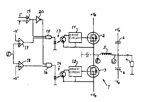
Turning firstly to Fig. 3, there is shown a circuit diagram of
the preferred embodiment of the invention. The diagram shows
a bridge circuit 1 comprising two transistors 2, 3 connected to
a load 4 through an LC filter 5, 6.
Several systems may be connected in parallel to the load. If
they have the same input signal, which is the preset value of
current, they will share the load current equally. The separate
systems do not have to operate in synchronism. Of course, several
bridge transistors 2, 3 can be connected in parallel.
The bridge voltage E at the connection point between the
transistors 2, 3 and the inductance 5 is shown by the diagram of
Fig. 1. If the lower transistor 3 is switched ON and then OFF, there
is provided a pulse during time period 7 and the bridge voltage E
immediately goes to minus. When the pulse is terminated, the
energy stored in the inductance must be released and forces the
voltage E to the opposite polarity during time period 8, i.e. plus,
and opens the flywheel diode of the upper transistor 2. When the
energy of the inductance 5 has been terminated, the flywheel
diode of the upper transistor 2 is blocked. However, the blockage
cannot take place immediately but a current in the opposite
direction must flow in order to charge or recover the flywheel
diode (reverse recovery current). This opposite current induces a
new but weaker magnetic field ln the inductance 5 which in turn
gives rise to an openlng of the fly-wheel diode of the first-
mentioned lower transistor 3 as shown at time period 9. Then, the
energy oscllla~es between the inductance 5 and the leakage
capacitances, primarily ~he transistor output capacitances (not
shown in Fig. 3) in the system as shown to the right during time
period 10 until attenuated.
It is pointed out that this sequence of events takes place due
to the fact that an LC-filter has been connected between the
bridge and the load.
It appears from Fig. 1 that the oscilloscope diagram after the
:,~
~9~53~
termination of the pulse is a damped oscillation, the amplitucle of
which being cut by the flywheel diodes at plus and minus the rail
voltage.
The present invention uses this sequence of events in order to
avoid or circumvent the above-mentioned problem. It is noted
that it should be completely safe to turn on the lower transistor
during the time period 9, while the lower flywheel diode is open
and the flywheel diode of the opposite transistor is closed. The
transistor then takes over the conduction from the flywheel diode
and a new sequence follows.
In Fig. 2 there is shown a timing diagram of the method
embodying the invention. According to Fig. 2, the upper
transistor is initially conducting (in Fig. 1 the lower transistor is
conducting). The procedure is completely the same and there is no
principal difference between the method using the upper or the
lower transistor. For positive output current the upper transistor
is turned ON and the flywheel current flows through the lower
diode. For negative output current the lower transistor is turned
ON and the flywheel current flows through the upper diode.
The upper diagram 2a shows the voltage E. It should be noted
that the time axis is not linear but is heavily expanded at the
rise and fall times. Diagram 2b shows the current I through the
inductance 5.
The upper transistor is conducting and the voltage E is at plus
during the time period I. The current I through the inductance 5
rises approximately linearly (actually exponentially). When the
current I reaches a preset value I', a first comparator changes its
state from loglc "I" to logic "O" as shown in diagram 2c. The
comparator controls the transistor and turns lt OFF and the
voltage decreases according to the swltching characterlstlcs of the
translstor as shown during tlme period II. The voltage E passes
below ~ero cand reaches minus and the flywheel dlode of the
negatlve translstor opens at the start of thetimeperiod III as
explained with reference to Fig. 1. The energy of the inductance is
terminated during time III and the current through the
inductance is reversed in order to turn OFF the flywheel diode of
the negative transistor (reverse recovery current). When the
r
-- 8 --
Elywheel diode of the negative transistor is turned OFF, the
voltage E rises during time period IV until the positive flywheel
diode opens. This rise of voltage is sensed by a second comparator,
which turns the positive transistor ON for a Eurther sequence
during time period V. The output of the second comparator is
shown in 2d. When the voltage E drops below -V', the comparator
outputs a logical "0" as shown. When both comparators are
outputting a logical "1", the positive transistor is turned ON. This
procedure will be further explained below in connection with Fig. 3.
It is noted that the switch frequency is not constant but is
high at low loads and decreases with increasing loads.
In Fig. 3 there is shown a circuit diagram of a presently
preferred embodiment of the invention. It is contemplated that
this circuit can be made at least partially as a custom designed
integrated circuit or Application Specific Integrated Circuit ASIC and
thus, the circuit solutions shown are only exemplary for
explaining the invention.
The bridge circuit is shown to the right in Fig. 3 as explained
above. Each transistor is driven by a drive circuit 11, 12. The drive
circuits are electrically isolated from the remaining control
circuitry by opto-couplers 13, 14 shown as a light emitting diode
and a photo transistor.
Each opto-coupler is connected to the output of an AND gate
15, 16 having two lnputs. One of the :Lnputs is connected to a first
comparator 19, which compares the actual current I through the
inductance 5 with a preset value 1'. When the actual current I is
below the preset value 1', the comparator 19 outputs a logLcal "1"
to AND gate 15, When ~he preset current I' is exceeded, the Olltput
from AND gate 15 is termlnated as shown at time II in Fig. 2 at 2c.
The transistor 2 is then turned OFF. The output from the first
comparator 19 is inverted by inverter 20 and connected to the
lower AND gate 16.
The second input of each AND gate 15, 16 is connected to a
second comparator 17, 18, corresponding to the second comparator
mentioned above. The comparator compares the voltage E with
preset limit values -V' and +V' (V'i9 a positive value),
respectively, as shown in Fig. 3. The positive comparator 17 (the
`~ '~:,;'"
. ~... _ .,
~?,~5~
- 9 -
upper) outputs a logical "1" when the voltage E is above the limit
-V' and the negative comparator 18 outputs a logical "1" when the
voltage E is below the limit +V'. Thus, there is a window between
+V' and -V' where both comparators output a logical "1". The
purpose thereof will be explained below.
In Fig. 4 there is shown a calculating circuit and a control
amplifier for calculating the actual current I and the preset
current I'. The preset value can be any value between plus and
minus the maximum bridge current. Consequently, the bridge
circuit is short-circuit proof. Although not shown, it is possible to
have an adjustable current limit.
The actual current (I) through the inductance can be
measured by conventional means, or calculated by analog or
digital circuits. If the difference voltage (E - U) across the
inductance is measured, the current (I) can be calculated according
to the following formula:
I = (E-U) / (R + s L)
where
I = inductance current
E = bridge voltage
U = output voltage to the load
R = resistance of the inductance
L = inductance
9 = Laplace operator
The resistance of the inductance should be as low as possible,
which however creates problem in the calculating circuit. The
calculation formula can be seen as a "transfer function" Eor the
calculating circuit. If R is small, the DC gain of the transfer
function is very high. Then any small but unavoidable offset in
the measuring or calculating circuits will be amplified to an
unacceptable value.
"-
- 10 -
It is possible to modify the calculating formula, by increasing
R for example 10 times, which decreases the DC gain and thus the
influence of possible offset voltages, and adjusting L so that the
calculated value will be approximately correct during the
maximum pulse time. Thus~ the calculating error ~ill be
significant only for times longer than the maximum pulse time,
which however is outside the operation area of the calculating
circuit and causes no harm.
A calculation circuit for calculating according to the above-
mentioned formula is shown in Fig. 4. The voltage U is subtractedfrom the volta ge E in a first OP-amplifier 21. The voltage U is first
inverted and scaled by inverter 22 and then connected to the
summing input of the OP-amplifier 21 at the negative input
thereof. The voltage E is connected to the same summing input
through a scaling resistance 23. The OP-amplifier is connected
substantially as an integrator according to the formula above and
integrates the difference between voltages E and U. The result is
the inverted inductance current (-I).
The preset current I' can be provided or generated in any
conventional manner. The actual current (I) and the preset
current (I') are transferred to the summing input of a fast
comparator 2~ and the output thereof is the difference between I
and I'. The comparator has very high gain and thus, the output
thereof is either high or :Low. The comparator is further provided
with a certaln hysteres by the resistances 25 and 26. The output
from the comparator ls inverted and buffered by the inverter 27
Eor providing Il - I which is the output signal provided by the first
comparator 19 in Flg. 3.
The circuitry of the entire system descr:Lbed above operates as
a current generator delivering output current to the load. It may
be used in this way with the preset value of the current I' as the
input control signal. However, it is often preferred to have a
voltage generator and the present system is easily converted to a
voltage generator. The output voltage U is measured and fed back
to a conventional PI-regulator (proportional integrating), the
output of which is the preset current I'. Such an integrating
" ,, ~ .
regu]ator will autvmatically correct Eor DC-offsets in the current
calculating circuit.
As shown in Fig. 4, the preset value Il of the current can be
calculated by a control amplifier from the actual output voltage to
the load U and a preset output voltage U'. A voltage corresponding
to the negative value of the preset output voltage U' is fed to the
negative input of a second OP-amplifier 28. The actual output
voltage U is also fed to said negative input through a scaling
resistor 29. The difference between the actual output voltage and
preset output voltage U - IJ' is substantially integrated by the OP-
amplifier 28 and the output thereof corresponds to the preset
current I' and is fed to the negative input of the comparator 24.
The zener diodes at the output of the OP-amplifier 28 limit the
maximum preset current I'.
In Fig. 5, there is shown a circuit corresponding to the
comparators 17 and 18 in Fig. 3. The comparators are made in TTL-
circuits and comprises three inverters 30, 31 and 32. The bridge
voltage E is fed to a first resistor 33 and 34 for each branch. A
voltage corresponding to the desired offset from the zero voltage is
fed to a second resistor 35 and 36 for each branch. ~ero voltage is
defined as midway between the positive and the negative rail. The
junction between the first and the second resistor is fed to the
input of one inverter 30 or 32, the input of which also being
grounded by a third resistor 37 and 38. The result is that when
the bridge voltage drops 50 that E -~ V' is below zero, the upper
inverter 31 outputs a logic "O" and closes the AND gate 15. When
the bridge voltage rises so th~t E - V' ls above zero, the lower
inverter 32 outputs a loglc "0" and closes the AND gate 16 (V' is a
positive value). The further operation should be evident from the
description in connectLon with Fig. 3.
IL the load Lmpedance ls too high (or the maximum output
voltage is too low) it is impossible to output the preset current to
the load in that case, the output voltage goes to maximum, and
the corresponding transistor remains constantly ON, which may be
undesirable. The maximum pulse time can be limited by two
retriggerable timers one for each bridge transistor.
In Fig. 6, there is shown a timer circuit 39 for terminating a
P~5~
- 12 -
pulse if the duration thereof exceeds a predetermined value
whereby each AND gate 15, 16 is provided with a third input,
which is connected to the output of a retriggerable timer, the two
trigger inputs of which being connected to the two other inputs of
the corresponding AND gate. If the inputs of the timer fails for a
certain time duration dictated by an RC-circuit ~0, the timer
outputs a logic "0", which terminates the pulse. Otherwise, the
timer outputs a logic "1".
It is evident that the current I is approximately triangular,
with the peak value twice the mean value. It is the mean value
that flows to the external load. If the switch transistors are
assumed to have constant ON resistance, the triangular current
waveform causes a power loss in the bridge transistors during
conduction that is 1/3 greater than it would have been with
rectangular current wavefrom.
It is also noted that the switching ON of the transistor takes
place when the current in the bridge is zero (or very close to
zero). This fact minimizes the power dissipation of the transistor
at the switch ON moment, which is an essential advantage. In this
apparatus, the transistors are always turned on at the right moment
when the opposite flywheel diode current is zero.
As mentioned above, there is a window, where both
comparators 17, 18 are outputting a logic "1". The reason for
this is that when the power is turned on to the circuit, the oscillations
must start. Dependent on tolerances of the components 21, 22, 24,
27, 28 etc, the output of comparator 2~ will be either high or low
at the initiation of the system. In either case, the corresponding
AND gate will be opened and the oscillations will start, since the
other input to both gates are at loglc "1".
It is noted in Fig. 2f that a lower firing pulse is generated
unintentionally. However, the duration of said firing pulse is very
short. In a practical circuit, the influence of this firing pulse is
slightly delayed and turns the lower transistor ON when the lower
flywheel diode is already conducting. However, when the preset
current is zero, the whole system will oscillate by help of these
short pulses. When one transistor is turned OFF, the other
, ~ .
i3~i
- 13 -
transistor is turned ON, then the first transistor is again turned
ON, etc. The pulse times will be dependent on the delays in the
various circuitry and the system will oscillate at a high maximum
frequency, which in the present embodiment can be around 300
S KHz.
It is also noted that the diagram in Fig. 2 is idealized in that
the time delays in the different circuitry is not taken account of.
However, such delays only improve the safety of the present
circuit and have no harmful influence. As an example, study Figs.
2c and 2d. If the rising edge in Fig. 2c occurs before the falling edge
in Fig. 2d, a new very short upper firing pulse will unintentionally
be generated. This is a type of electronic "race" that sometimes
occurs in pulse circuits. Of course, the designer must observe the
possibility of such situations and take appropriate counter
measures. In this sytem, it is noted that it is only necessary that
the transistor is turned on during the time period 9 in Fig. 1.
Thus, there is sufficient time for any delays.
It is also noted that the bridge system is able to operate in a
generative as well as a regnerative mode, feeding energy to the
load or receiving energy from the load back to the power supply
rails.
Hereinabove, a preferred embodiment of the invention has
been described in details. However, it is clear to a skilled person
that many details may be modified without departing from the
scope of the invention. For example, the sensing of the direction of
change of the bridge voltage ~ can be determined by a
differentiator instead of a comparator. It may be possible to
replace the senaing of the voltage change by sensing when the
current in the bridge or lnductance ls zero and firlng the
transistor shortly thereafter.
The present embodlment has a rail voltage of about 2 x 155 V
and a maximum output current of 25 A (mean value 12.5 A). The
lnductance is approximately 40 ~H and the resistance of the
lnductance is about 10 mQ . The capacltance ls about 10 ,uF. It ls
preferred to cormect the capacltances to both ralls, in which case
the capacitors also fllter the rall voltage. The magnetic fleld in
the inductance is about 0.2 T. The frequencies are from about 1 -
1000 ICHz, preferably from 5 - 300 ~Hz and change depending on
the load. The above mentioned values are only given as example
and can be modified within large limits when improved
components are manufactured, specifically the semiconductors and
the inductance core. The load can be connected between the
output and ground or in any other conventional manner to other
legs in the bridge system.
An apparatus embodying the present invention is useful for
delivering output voltage and current of both polarities. If only
one polarity is required, as for example in conventional DC power
supply units, the invention can still be used. Then, all those
components, which are necessary for the opposite polarity, can be
removed, resulting in a simpler circuit.
Further modifications should be obvious to a skilled person.
The invention is only limited by the appended claims.
~ ,. . f