Note: Descriptions are shown in the official language in which they were submitted.
~29~S~
P~IN i2.035 l 8.8.19~7
Radiation~sensitive semiconductor device.
The invention relates to a radiation-
sensitive semiconductor device comprising a semiconductor
body in the form of a wafer having a thicker edge portion
and a thinner central portion provided with a substantially
flat first surface and an oppositely arranged second
surface extending substantially parallel to the first
surface, this device comprising a high-ohmic first region
of a first conductivity type adjoini~g the first surface,
a second region of the second opposite conductivity
type which is arranged within the central portion, adJoins
the first surface and forms with the first region a
photodiode comprising a radiation sensitive pn junction
and is entirely surrounded by the first region within the
semiconductor body, as well as a highly doped contact
layer of the first conductivity type adjoining the
second surface and the first region, a metal layer being
for~.ed on at least a part of the second surface~ and the
metal layer and the second region being provided with
connection conductors, while the central portion of the
semiconductor body i9 SO thin that it i9 depleted at
lea.st as far as th.e contact layer when a voltage of less
than 10 V is applied in the reverse direction aaross
said pn ~unction.
The invention further relates to a method of
manufacturing such a semiconductor device.
............. ... .
A semiconductor device of the kind described
is known from the French Patent Application published
under No. 22OL~9~9.
Semiconductor devices comprising photodiodes
are known and are used in radiation-sensitive circuit
arrangements and apparatuses of different ~inds, for
example for optical communication, for optically recording
and reading information and for various computer applica-
PHN 12.035 2 8.8.1987
tions. In most cases, it is of major importance -that
the photodiode is rapid, i.e. can ~ollow variations of
radiation intensity having a very high frequellcy ( ~ 500 M~k~
Another important fact is that in many cases
it is desirable and even necessary that the photodiode
can operate at low voltages of, for example, less than
5 V.
In order to obtain a rapid photodiode, the
diode capacitance should be low, which can be achieved in
that the diode is formed on semiconductor material of very
high resisti-vity~ However, it has been found that in most
cases also a slow component occurs, which is due to
diffusion of generated charge carriers from the substrate.
More particularly with high-ohmic material, in which the
life of minority charge carriers is generally long, this
diffusion can take place from parts located at a compara-
tively great depth. In the semiconductor device according
to the aforementioned French Patent Application 22&4989,
the central portion is thin-etched so that this portion is
20 fully depleted already at a low volta~e across the photo-
diode. Thus, a photodiode operating at a low voltage is
obtained, in which in the thin central portion only the
thin contact layer adjoining the second surface can
contribute to the aforementioned slow signal
25 component. However~ parasitic charge carriers can also
diffuse to the surroundings o~ the photodiode from the
-thicker non-depleted edge portionsof the wafer and thus
can nevertheless give rise to a not unimportant slow
component.
The invention has inter alia for its object
to provide a radiation-sensitive semiconductor device
comprising a rapid photodiode which has a high sensitivity,
operates at a low voltage and is mechamicall~ strong.
According to the invention, a radiation-
35 sensitive semiconductor device of the kind described in
the opening paragraph is characterized in that the metal
layer is reflecting for the radiation to be detected
~L~9~S~;~
P~ l2.035 3 8.8.1987
and in that a screening diode adjoining the first
surface is provided, which entirely surrounds the second
region within the central portion, extends into the
thicker edge portion and is entirely surrounded by the
first region within the semiconductor body, the
screening diode forming with the first region a
rectifying junction and being provided with a connection
conductor for applying across the screening diode such a
voltage in the reverse direction that ths depletion zone
thus formcd extends in the central portion at least as far
as the contact layer.
Due to the fact that the depletion ~one
starting from the screening diode en~irely depletes the
edge of the cnntral portion of the s~miconductor wafer as
far as the highly doped contact layer, this central
portion is practically insulated electrically from the
edge pcrtion. As a result, the charge carriers generated
in the central portion by radiation not incident upon the
photodiode and also those charge carriers which are
generated (opticaly or thermally) in the high-ohmic edge
portion of the wafer and diffuse towards the photodoide,
are drained via the screening diode, except for a very
small part which can diffuse via the contact layer. The
said slow signal component is then consequently practically
eliminated. Due to the high-ohmic material used, the
capacitance of the photodiode is low, which leads to an
increase in speed. Moreover, the depletion of the central
portion is attained at a ve~ low voltage (with the use
of n-type silicon of 1000 Q .cm and a thickness of
10/um for the cen-tral portion for example only 2 V). The
metal layer on the second surface ensures a high sensitivi-
ty by reflection of the inc~dent radiation.
The screening diode can comprise a metal layer
which forms a rectifying junction with the first region.
According to a preferred embodiment, the screening diode
forms with the first region a pn junction, which can
then advantageously be formed simultaneously with the
~9~5~L
p~ 12.035 4 ~.8.1g87
radiationcensitive pn junction of the photodiode.
Pre~erably, the screening diode covers
substantially the whole edge portion and the major part
o~ the central portion o~ the semiconductor body~ Further,
the distance between the radiation-sensitive pn j~mction
and the screening diode is preferably so small that in
the operating condition the depletion zones associated
with the screening diode and with the photodiode touch
each other or even overlap each other under the influence
of the then prevailing operating voltages. Under these
conditions, diffusion of parasitic charge carriers is
counteracted as e~fectively as possible.
The radiation may be incident upon the ~irst
sur~ace or upon the second sur~ace~ In the latter case,
the re~lecting metal layer is provided with an opening
serving as a window ~or the incident radiation.
The semiconductor body may consist o~ a
semiconductor element, such as silicon or germanium, or
o~ a semiconductor compound, ~or example a III-V compound,
such as galliumarsenide. However, the semiconductor body
pre~erably consists o~ silicon and the ~irs-t region has a
doping concentration o~ at least 10 1 and at most 10 3
atoms per cm3. Preferably9 the ~irst region consists of n-
type conducting silicon having a resistivity of at
least 1000 Q .cm.
The thlckness o~ the central po~tion o~ the
body will then generally be at most 200/um in order to
ke~p the operating voltage low. Pre~erably, the thickness
o~ the central portion will not exceed approximately 10/~m.
'rhe invention will now be described more
~ully with rererence to an embodiment and the drawing, in
which:
~ig. 1 shows diagrammatically in cross-section
a semiconductor device according to the invention taken
on the line I-I o~ Fig. 2,
Fig. 2 shows diagrammatically in plan view
the semiconductor device o~ Fig, 1, and
Fig. 3 shows diagrammatically in cross-
~;29~55~
PHN 12.035 5 ~,8.1987
section another embodiment of the semiconductor deviceaccording to the invention.
The Figures are purely schematic and are not
drawn to scale. Semiconductor regions of the same
conductivity type are cross-hatched in the same direction,
In the plan view of Figo 2, the metallization is indicated
by cross-hatched lines.
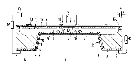
~ ig. 1 shows diagrammatically in cross-
section and
Fig. 2 shows in plan view a radiation~sensitive
semiconductor device according to the invention, The device
comprises a semiconductor body 1 of silicon in the form of
a wafer having a thicker edge portion 1A and a thinner
central portion 1B. The wafer has a practically flat first
surface 2 and an oppositely arranged second surface 3
extending substantially parallel to the first surface 2.
In the plan view of Fig. 2, the boundary between the parts
1A and IB is indicated by a dotted line 15,
The device comprises a high-ohmic first
20 region 4 of a first conductivity type, in this embodiment
an n-type conducting region having a resistivity of
1000 Q .cm, which adjoins the first surface 2. Further,
the device comprises a second region 5 of the second,
opposite conductivity type~ so in this embodiment of the
conductivity type, which is located within thecentral
portion IB and adjoins the first surface 2. The region 5
forms w:Lth the first region 4 a photodiode comprising a
radiation-sensitive pn junction 6; the region 5 is
surrounded entirsly by the first region 4 within the semi-
conductor body, The device further comprises a highlydoped contact layer 7 of the ~irst, so in this case n,
conductivity type adjoining the second surface 3 and the
first region 4. ~ metal layer 8 is provided on at least a
part of the second surface 3, in this case on the whole
35 surface. The metal layer 8 and the second region 5 are
provided with connection conductors 9 and 10. The central
portion 1B o~ -the semiconductor body is so thin that it
.5~
PHN 120035 6 8.8.1g87
is depleted at least as far as the contact layer 7
when a reverse voltage Vl of less than 10 V i~ applied
across the pn junction 6. The signal is measured across an
impedance Ro
A radiation-sensitive device as described thus
far is known from the aforementioned French Patent Applica-
tion published under No. 2284989.
According to the invention, the metal layer 8
is reflecting for the radiation to be detected and the
device is provided with a screening diode 11, which adjoins
the first surface 2, entirely surrounds the second region 5
within the central portion 1B, extends into the thicker
edge portion 1A and is surrounded entirely by the first
region 4 within the semiconductor body. In this embodiment,
the screening diode is constituted by a p-type conducting
zone 11, which forms a pn junction 12 with the first region
4. The screening diode covers substantially the whole
surface of the edge portion 1A of the wafer. The screening
diode 11 is further provided with a connection conductor 13
for applying across the screening diode such a voltage ~2
in the reverse direction that the depletion zone thus
formed extends in the central portion 1B at least as far
as the contact layer 7.
In the semiconductor device according to this
embodiment, the radiation is incident upon the surface 2 in
the direction of the arrows 14.
In the operating condition, the situation is
that indicated in Fig. 1. The depletion zones o~ the
screening diode 11 and of the photodiode 5 are indicated
by the non-cross-hatched part of the region 4 bounded bv
a dottecl line 16. The depletion zone insulates the
central portion 1B electrically from the undepleted part
of the thicker edge portion lA, from which no charge
carriers can diffuse to thecentral portion 1B other than
via the thin contact layer 7. Thus, the aforeman-tioned slow
signal component is practically avoided in the semiconductor
device according to the invention, the more so as the
5Sa~
RHN 12.035 7 8.8.l987
diffusion leng-th of charge carriers is small in the very
highlydoped ( ~ 102 cm 3) contact layer 7.
A further advantage of the invention is that
radiation incident outside the central portion does not
in~luence the opera tion of the diode,scattered light
and other undesired light only produces a current in the
circuit in which V2 is included. Detection of this current
via an impedance R' may be used, for example~ to align
a fibre, from which the light 14 emanates, to the
central portion. The signal measured via the central diode
across the impedance R is then a maximum and at the same
time the signal measured across R' is a minimum. In
general, R' is tharefore a temporarily present impedance
for adjustung the device.
In this embodiment, the first region 4
consists of n-type silicon having a resistivity of 1000 Q .
cm, i.e. a doping concentration of about 4.6 . 10 2
atoms per cm3. The edge portion lA has a thickness of 385
/um; the central portion 1B has a thickness of 10/um. The
second region 5 constituting the photodiode has a thickness
of 0.2/i~m and in this embodiment has a 0.8/um thick
edge at the area of the annular contact 10. The zone 11
constituting the screening diode has a thickness of 0.8/um.
In order to obtain a better definition of the potential
25 variation at the outer edge of the region 12, an n~
conducting zone 17 is provided along this edge. The n-
type contact layer 7 has a thickness of about 1/um.
~ nder these conditions, the central portion 1B
is entirely depleted at voltages of at least 2 ~ across
30 both the photodiode and the screening diode.
The semiconductor device of the embodiment
described can be manufactured in the following manner.
The starting material is a (100) orientated n-type silicon
wafer having a resistivity of 1000 5~ .cm and a thickness of
35 about 400/um. This wa~er is thermally oxidi~ed and channels
are then etched at a surface into the oxide 18 by means of
known photolithographic techniques between the separate
~q~
P~ 12.035 ~ 8.8.1987
devices to be ~rmed on the silicon wafer. The thickness of
the oxide 18 is chosen so that with any ~urther silicon
nitride layer to be applied nr any other coating at least
on the central portion of the device the transmission for
the light used is an optimum. For forming the said zones 17,
a heavy phosphorus diffusion is provided in these channels.
However, this is not necessary.
Subsequently, the regions 5 and 11 are formed
in kno~n manner in the same surface by ion implantation.
If desired, these regions may be formed in a single step,
but in connectiQn with the smaller depth of the active part
of the photodiode two implantation steps are used in
this embodiment. The diame-ter of the~photodiode is in
this case 100 /um; the distance between the zones 5 and 11
is 10/um. After impl~ntation and a diffusion step, a
silicon nitride layer having a thickness of 1/um is
deposited on the silicon wafer as a mask. Subsequently,
a square region of 800 x ~00/um2 is exposed on the back
side of the wafer and the silicon is etched selectively
for about 10 hours in a solution of ~O~I and propanel in
water in order to obtain the desired thickness of the
central portion lB. The central portion is then bounded by
(111) surfaces at an angle o~ about 57.
Subsequently, the silicon nitride is removed and
the silicon wafer is subjected to a phosphor~ls diffusion,
the contact layer 7 then being formed. This phosphorus
deposition at the same time serves as a gettering step.
The required contact windows are then etched
and the metallization is provided in the usual manner~
30 For this purpose, an aluminium silicon layer containing
about 1 /0 ofsiticon is used in this embodiment. The
assembly is then provided in a suitable envelope.
In the present embodiment, the screening diode
is constituted by a ~-type zone 11. Instead thereof,
35 a Schottky diode could also be used, which may be consti-
tuted by a suitable metal forming a rectifying junction
with the weakly n-type conducting region 4
L55~
p~ 12.035 9 8.8.1987
Instead of being incident upon the surface 2,
at which the photodiode is situated, the radiation l4
may also be incident upon the opposite surface 3. The metal
layer 8 disposed thereon must then have an opening serving
as an entrance window and if desired, an anti-reflection
coating of, for example~ silicon monoxide may be provided
therein (not shown here). The situation then becomes that
shown in Fig, 3, while in the n-type contact layer also an
opening may be provided at the area of this window in order
lO to avoid unnecessary recombination. The other surface 2 is
then coated over a largest possible part with re~lecting
metal (10, 13) in order that ~e maximum number of photons
can be converted into charge carriers. In the case in
which radiation incident from both sides has to be detected,
l5 an entrance window may be provided both in the metal layer
8 and in the metal layer 10.
The invention is not limited to the embodiments
described above. ~or example~ the dimensions of the various
semiconductor zones and regions may be varied within wide
20 limits on tha understanding that the depletion zone of the
screening diode should extend bo-th within the thinner
central portion and within the thicker edge portion. Other
semiconductor materials and other reflecting metals may
also be used, while the thickness of the various regi~ns and
25 layers may also be chosen differently.