Note: Descriptions are shown in the official language in which they were submitted.
/ ~9~Z~8~
24266/MOLD-18
.
PHOTORESPONSIVE ~ECTRODE FOR DETERMINATION
OF REDOX POTENTIAL
The invention concerns electronic devices for
measuring redox potential in an electrolyte and for
10 measuring the rate of change in redox potential in
electrode~ containing an analyte where the analyte is
made to effect a change in redox potential.
Industry, medicine, and other areaa are fre-
quently involved with the meaqurement of a continuously
extending list of analytes. There exists today a large
number of dlfferent de~ice~ and protocols for deter-
mining analytes in process ~treams, physiological
20 ~luid~, and environmental substances. Each of these
devices has a variety of advantages and di~advantage~.
In any device, one is concerned with the economics of
its production, it~ ~ensitivity, reliability, lifetime,
ease of use, and adaptability to di~ferent media and
analytes.
One of the problem a~sociated with ~ensitive
~easurement of redox species or redox react~on~ with a
redox electrode is that 3tray currents within the elec-
$rochemicaljmeasurement cell or within the c$rcuitry
attache~ to the redox electrode introduce error into
the measurement. Such 3tray currents may ari3e from a
number of ~ources including corroslon reactions within
~he cell, electrical Yhort circuit~, or pickup of elec-
trical noi~e ~rom the environment. It i3 therefore
desirable to mlnim$ze these sources of mea~urem0nt
error by using corr~sion reslstant material~ and by
smploying mea~uremen~ devlces and c$rcuitry configura-
'
2~3~
t~on~ which reliably minlmize stray currents. Addi-
tionally, in aqueous envlronments, another problem
associated with sen3itive measurement of redox specie~
is the need for a stable, llquid ~unction, re~erence
electrode. Such reference electrode~ are co~tly and
inconvenient to pro~lde in otherwise ~olid- tate mea-
surement deviceR. Al~o, reference electrodes can be
unreliable in commercial use, because variouq reference
electrodes, such aR liquid re~erence electrode3 ~end to
show dri~t ln potential. In this ~ituation, one mu~t
~ind some way to compensate for the change in potential
of the reference electrode in order to be able to com-
pare re~ults obtained at di~ferent times. There is
therefore, an interest in f1nding techniques to obviate
the need for a liquid reference electrode or provide an
alternative standard of reference.
U.S. Patent No. 4,490,216 describe~ a lip~d
membrane containing electronanalytical element. U.S.
Patent No. 4,591,550 de~cribes the use o~ monolithic
~emiconductorq ~or determining a plurality of ~amples
at different ~ites on the semiconductor, interrogat~ng
variou~ ~ite~ Or the ~emiconductor with light. U.S.
Patent No~. 4,020,820, 4,322,680, and 4,397,714
describe the use of chemically-sensitiYe field effect
transl~tor~ to detect redox compound~.
Methods and photore~pon~ive field effect
device3 are provided for detecting a wide variety o~
analytes, employing a photoresponsi~e substrate in
connection with a metal electrode. Preferably, the
metal electrode is in the form of a metal layer posi-
tioned on the surface of an ln~ulative layer, which in
turn is po~itioned on the photore~pon~lYe substrate.
The sample medium lnclude~ a redox couple, where the
potential o~ the red~x couple may be related to the
~tandard potential of the redox couple and the ratio of
reduced and oxidlzed member~ of the redox pair. The
pre~ence and amount of an analyte may be detected by
it~ ef~ect on the ratio Or reduced and oxidlzed members
of the redox pair and thus upon the redox potential.
Measurements are made on the medium by photo-
responsively monitoring eleetrlcal-field-effects within
a ~urface region o~ the photorespon~lve ~ubstrate,
10 where the potential on the isolated metal electrode
a~fect~ the e~ectrical field w1thin ~uch region.
Various measurements may be employed to monitor photo-
responslvely electrical-field-ef~ects within 3uch
region o~ the photoresponsive substrate, including
15 monitoring photoconductance, photocapacitance, photo-
voltage, or photocurrent.
The need for a liquid junction reference elec-
trode i~ obviated by monltoring photoreqponsively both
a) the redox potential at a fir~t surface region Or the
photorespon~ive ~ub~trate, where the electrical ~ield
i~ influenced by the redox potential of the medium in
contact with t~e metal layer; and b) monitoring the
electrical field at a ~econd surface region o~ the
photore~pon3ive ~ubstrate, where the electrical field
i~ ~ubstantially independent of the redox potential of
the medi um or vari es in a know~ manner di~rerent ~rom
the variation at the first siteO The respon~e as mea-
~ured at the fir~t and ~econd ~ite~ may be compared 50
a~ to determine the relative difference in redox poten-
tial of electrolytea of dif~erent compo3ition pre3entat the ~ir~t and ~econd site~ or to determine the
change in redox potential over time at one ~ite with
re~pect to the electrical rield at the other ~Ite.
In the drawings:
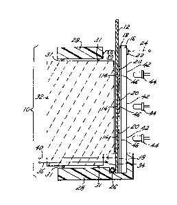
Fig. 1 i3 a diagrammatic cro~s-3ectional view
of a device according to thi~ invention;
~Z~2;2~
Fig. 2 i~ a plan view of a multiunit device
according to Fig. 1;
Fig. 3 is a diagrammatic view of a single unit
device;
Fig. 4 i3 an exemplary circuit ~or use with
the device;
Figs. 5 and 6 are graph~ of the results
obtained with a ferri/ferrocyanide couple with the bias
potential an ordinate and the alternating photocurrent
as absci3sa, with ~ig. 6 as the second derivati~e of
the graph of Fig. 5;
Fig. 7 is a graph of the effect of the alter-
nating photocurrent amplitude as a function of bias
potential when the redox potential of the electrolyte
i~ altered by changing the ratio of ferricyanide to
ferrocyanide anion concentration;
Fig. 8 shows the change in ~0" as a function
o~ the logarithm of the [ferricyanide]/[ferrocyanide3
ratio;
Fig. 9 is a graph of the alternating photo-
current amplitude as a function of bias potential ~or
elctrolytes at pH 4, 7, and 10;
Fig. 10 is a graph of the change in ~O'r as a
function of pH;
Fig. 11 is a graph oS the alternating photo-
current amplitude a~ a function of bias potential
resulting from illumination of both redox potential and
pH sensitive regions of a photoresponsive electrode;
Fig. 12 i~ a graph of the first derivative of
3 the result9 of Fig. 11;
Fig. 13 i~ an alternatire circuit ~hown with a
diagrammatic view o~ a device which permit3 redox
potential mea~urement without a 3eparate re~erence
electrode;
Fig. 14 is a graph of the difference in bia3
potential between the two minima in the ~irst derlva-
tive of the alternating photocurrent amplitude V5. biaY
~.Z~`2Z~
potential response where the circuit and device as
shown in Fig. 13 were employed while the pH is kept
constant at 7.0 and the redox potential was varied;
Fig. 15 is a graph o~ the difference in bias
potential between the two minima in the ~irst deriva-
tive of the alternating photocurrent amplitude vs. bias
potential response where the circuit and devioe as
shown in Fig. 13 were employed while the pH is raried
and the redox potential i~ held constant; and
Fig. 16 is a circuit and a diagrammatic Yiew
of a device for u9e in photoresponsive amperomeSric
determinations.
~ N~ E~ E~ IG~M~Q~IME~IT~
15 Electrochemical methods and photoresponsive
devices are provided ~or determining the state o~ an
electrolyte medium where the ~tate affects the measured
redox potential of the medium. The redox potential of
the electrolyte medlum is monitored with an electro-
chemical measurement cell employing two or more elec-
trodes. The first electrode 1s a working electrode
comprised of a photoresponsive ~ubstrate with an elec-
tronically conductive layer in contact with the
electrolyte. In the preferred modet an electrically
insulating layer i9 placed between the photoresponsive
substrate and the surface of the electronically conduo-
tive layer. The in~ulating layer is sufficiently thin,
so that the potential of the electronically conductive
layer substantially affects the electrical field within
a surface region of the photoresponsive substrate.
Also, in one embodiment, a portion of the insulating
layer i~ free Or the electronically conductive layer,
so as to be in direct contact with the electrolyte to
provide a redox potential independent photoresponse.
The second electrode may be a potential-stable, liquid
~unction re~erence electrode or a le~s potential-stable
controlling electrode. Alternatively, both the refer-
~22~
ence electrode and the controlling electrode may beemployed together with the working photoresponsive
electrode to form a 3-electrode electrochemical cell.
The redox potential of the electrolyte deter-
mines the potential of the electronically conductive
layer on the working electrode. The potential of the
electronically conducti~e layer in turn determines the
magnitude and direction of the electrical field within
a ~ur~ace re~ion of the photoresponsive substrate. The
magnitude and direction Or the electrical ~ield may be
monitored by a variety of photoresponsive measurements.
The photoresponsive measurements provide a measurement
of the redox potential of an unknown electrolyte medium
relative to a redox potential of a standard electro-
lyte, which may be introduced as the electrolyte
medium. Multiple photoresponsive measurements may be
made sequentially over time, so a~ to provide informa-
tion as to the rate of redox potential change of the
medium over time.
By employing either a plurality of electrodes
or a plurality of irradiation ~ite~ on a single elec-
trode, substantial flexibility may be achieved in mea-
suring two or more states of a conducti~e mediumO The
states may involve redox potential, pH, concentration
25 of a solute, presence o~ a particular moiety, volume,
temperature, or other variable, which can be detected
either dlrectly or indirectly by a photoresponsiYe
electrical measurement.
The device employ~ light means for interroga-
30 ting one or more ~ites o~ the working electrode. A
circuit i~ provided for determining the signal produced
by irradiation o~ the working electrode, where the sig-
nal will be related to the redox potential, the pH, or
other ionic components of the medium. These ~ignals in
35 turn may be related to another state of the medium.
~2~
The methods employ a wide variety of ~ystems
which allow for variation in the redox potential, pH
state, or other ionic composition ~tate, of the medium
in relation to the state o~ interest, particularly the
concentration of an analyte or the presence of a parti-
cular moiety.
The device which is employed may have one or a
plurality of working electrodes, each wlth one or more
sites for irradiation, and at lea~t one electronically
conductive layer a~soeiated with at lea~t one o~ the
working electrodes. Each of the working electrodes will
have an ohmic contact or connection to a circuit, where
individual working electrodes may have a common connec-
tion to the circuit. Alternatively, the individual
working electrode may have individually ~witched con-
nections to the circuit, so that each of the working
electrodes may be electrically isolated.
Nor~ally, the sample will contact each of the
electrodes, and preferably the ~ample will contact both
the electronically conductive layer and the working
electrode surface free of the electronically conductive
layer. The working photoresponsiYe electrode may or
may not have an insulative layer 9 but in order to
obtain a potentiometric rather than an amperometric
mea~urement, where an insulati~e layer does not provide
the high re~istance, the circuit requiras some other
high re~istance element. Hereafter the electronically
oonductive layer may be referred to as a metal layer,
although it ~hould be understood that electron
conductor~ other th~n metals ~ay al~o be used.
The measurement Or the redox potential, pHI or
other ionic compo~ition of the medium are indirect
potentiometric mea~urements, where the photorespon3ive
parameter, preferably photocurrent or photovoltage~ may
be measured directly. In this way, if the redox poten-
tial, the pH, or the ionic compo~ition i3 fixed a~ a
referencel by providing ~or a ~ub~tantially invariant
~2'~8C~
state o~ the particular medium components during the
period of measurement, the remaining variables may be
determined as a function of time. In this manner, a
reference electrode, which provides for a atandard
potential, i3 not required. Incorporation of such
reference electrode, howeYer, allows a separate deter-
mination of the medium component of interest to be
made. Thu~, a ~ariety of physical or chemical states
o~ the medium may be normalized.
Such variables as volume, temperature, solute
acitivity, or the like may be determined. For example,
a fixed amount o~ reactant, e.g., enzyme, which pro-
duces a known change in pH or redox potential over a
predetermined time period in relation to the reference
electrode and a predefined set of conditions, can be
used to determine a change in one of the conditions,
where the other conditions are held constant.
The device will provide ~or photoirradiation
of the working electrode at one or more sites associ-
ated with the region under the electronically conduc-
ting layer and with the region under an area free of
the electronically conducting layer. Photoirradiation
may occur simultaneously at both regions, particularly
regions contiguous to each other, or sequentially.
For potentiometric mea~urements, one may
employ a ramp in bias potential and measure the photo-
response, e.g., photovoltage or photocurrent, as a
function of the bias potential ~alue. Where two or
more sites are illuminated sequentially, results of ths
measured photoresponses versus bia~ potential relation-
ship are obtained for each site. Nhere two sites haYe
a metal layer in contact with the electrolyte, a
~tandard redox potential electrolyte may be provided at
one, or more, of the sites so as to provide an internal
redox potential ~tandard at at least one site. The
redox potential of an unknown assay medium may be
determined at one or more sites that are di~erent ~rom
~z~o
the sites of the standard. The metal layer~ ~sociated
with each independent site may have any shape or form;
however, it i~ important that the metal layerq are not
connected one to another by any substantially
5 conductive material other than the electrolyte medium.
Alternatively, one or more of the ~ites a~so-
ciated with the illuminated regions of the working
electrode may have the metal layer omitted. In place
of the metal layer at these sites a pH-responsive or
10 other specific ion-responsive surface may be provided
instead. With this alternative, the pH or other speci-
fic ion composition may be maintained fixed at one or
more of the sites away from the metal layer so as to
proYide an alternative internal potential standard.
15 Where the redox potential, pH, or specific ion state of
the medium is fixed at one or more site~, any variation
in the observed photoresponse versus bias potential
relation~hip can be related to either a change in the
state of the medium or to ~ change in the mea~urement
20 system. Incorporation of the internal reference stan-
dard allows the~e changes to be determined indepen-
dently, thereby permitting changes in the measurement
system to be subtracted from the obser~ed photoresponse
versu~ bias potential relationship yielding the re~ult
~5 of interest. In this manner, one can correet for
change~ in conditions other than the change o~
interest.
In carrying out the a~ay, the as~ay medium
may be prepared by adding the appropriate reagents,
3 which will provide for either a constant redox poten-
tial, a con3tant pH, or other constant lonic moiety
composition of a medium during the period of mea~ure-
ment. Where an analyte is being measured, the analyte
may be a component of the redox couple, or may react
with a component o~ the radox couple, or may influence
the redox potential of a redox couple. Alternatively,
the analyte, or a product re3ulting from the analyte,
:!L2~2~
1 0
may affect directly or indirectly the pH or other ionic
compo~ition of the medium. Depending upon the particu-
lar analyte of intere~t, the analyte itself may be
mea3ured directly or may serve to influence a medium
component to provide a change in the observed photo-
re3pon~ive electrical signal ralated to the amount of
analyte.
In all cases, the electrodes are contacted
with the sample, so that the sample forms a conducting
bridge between the counterelectrode, the photorespon-
slve working electrode, and, optionally, the reference
electrode. The working electrode i5 then illuminated
so as to producs excess minority charge carriers in a
surface region of the photoresponsive substratum of the
working electrode where the electrical ~ield is sub-
stantially af~ected by the potential of the metal
layer. The electrical signal, i.e., the photorespon-
sive ver~us bia~ potential relation3hip, may be com-
pared to a ~tandard relationship for a defined set of
conditions to determine the redox potential of the
medium. One may illuminate, in addition, a region of
the working electrode displaced from the metal layer.
Exce~s minority charge carriers in such sur~ace region
of the photoresponsive substratum o~ the working elec-
trode may be produced, where the electrical field issubstantially af~ected by the potential at such site on
the working electrode surface. This site may be com-
prised of an insulator with a pH-respon3ive surface so
aQ to produce an electric field within a surface region
of the photorespon~ive substratum that i~ pH-respon-
sive. Alternatlvely, either the insulator or base
photoresponsive substrate may be coated with a
specific-ion-responsive membrane, so a~ to produce an
electric field within a surface region of the photo-
responsive substratum that is respon ive to a ~pecificion within ~he medium. Such ion-~elective membranes
are well known in theory and operation. See, for
~~t'2~
1 1
example, Steiner, et al., Anal. Chem. (1979) 51:351,
and references cited therein. Ionic analytes of inter-
est include lithium, potas~ium, calcium~ ce~ium,
ammonium, sodium, chloride; fluoride, sulfide, both
5 cations and anions.
The electrical ~ignal, i.e., the photoresponqe
~ersu~ bias potential relationship, may be obtained
separately in the redox qen~itive region (i.e., the
region coYered with the metal layer) and in the pH or
10 specific ion ~ensitive region. These separately ob-
tained signal~ then may be compared in order to derive
a relationship between redox potential and pH or ionic
composition of the medium. By repeating both the above
measurement and compari~on steps over time, one may
5 deduce the rate o~ change in the relationship between
redox potential and pH or ionic Gomposition over time.
Because the preci~ion of determining the relationship
or rate of change of the relationship is independent of
the re~erence electrode potential, a potential-stable
20 reference electrode i9 not required for precise
measurement of the relationship or rate of change in
the relationship over time.
Con~eniently, one may illuminate a region o~
the photorespon~ive electrode a~sociated with the bor
25 der between the metal surface layer and the surface
free of such layer. In this event, one obtains a
stepped photore~ponse upon ramping the bias voltage.
The initial step in the photoresponse is related to the
potential either of the surface metal layer or the
3 sur~ace free of ~uch metal layer. The second ~tep, is
related to the potential of the remaining surface
(i.e., the one o~ the two above ~urfaces which was not
related to the initial step) as~ociated with the
illuminated region of the photoresponsive electrode.
As long a~ the initial and second step~ are suffi-
ciently ~parated in applied bias potential voltage ~o
as not to interfere with each other, each of the
z~
12
individual sur~ace potentials, or change thereof with
re~pect to time, may be determined. This convenient
method offers the advantage of employing only a ~ingle
beam of illumination and employing only a ~ingle ramp
in applied bias potential ~or each multiple
determination of ~urface potentials. The advantages
g$ven above for determination of at least two
parameters, such as redox potential and pH, for
example, are maintained with this convenient and ~imple
method.
The photore~pon~ive working electrode gener-
ally will be compo~ed of semiconductor or photocon-
ductor materials, such as silicon, which may be a
single crystal, polycrystalline or amorphous, gallium
arsenide, gallium ~elenide, aluminum gallium arsenide,
chlorogallium phthalocyanine or the like. The semicon-
ductor material will be either of the p- or n-type and,
as appropriate, and ~ay employ such dopants as boron,
aluminum, phosphorus, arsenic, antimony, or the like.
The degree of doping may be varied widely, there being
a wide variety o~ commercially-available doped wafers
which can be used, where the body of the wafer i9
lightly doped and portion~ of the wafer heavily doped.
The doping will be sub~tantially uniform adjacent to
the surface in contact with the sample. There also are
available arrays of individual microchips which are
insulated one from another which may be ~oined to a
common circuit with or without qwitching elements con-
necting the individual chipq to the circuit. The con-
centration of the dopant normally will vary empirically
to provide the de~ired re~ponse, frequently being a
matter Or convenience, and generally will range ~rom
about 1012 to 1018 atoms~cc, usually ~or silicon, the
re~i~tivity will be about 0.01-1000 ohm-cm.
Where the monolithic wafer~ are u~ed, they may
come in a variety of size~ and ~hapes, varying from
chip 3ize which may have its largest dimension o~ at
least about l.Omm, u~ually 2mm; or wafer size, which
may be 500mm, more usually not more than about 100mm in
its largest dimension. The electrode region uqually
will have at least one smooth sur~ace or smooth portion
o~ a surface, desirably flat, which will serve as the
electrode surface. The wafer may be round, rectangu-
lar, elongate or the like. The thickness of the chip
or wafer generally will be not more than about 2mm,
usually less than about lmm, and generally not less
than a~out 0.0~, usually not less than about 0.1mm.
An inqulative layer normally is employed to
cover the exposed working electrode regions, which
layer usually will be coated uniformly. The signifi-
cant factor is that the ~emiconducting portion of the
working electrode is insulated electrically and chemi-
cally from the medium by some means. Conveniently, a
coating of silicon oxide and/or silicon nitride can be
employed, generally of from about 200 to 2000A, prefer-
ably from about 600 to 1500A to provide for the in~ula-
tive layer. The silicon oxide or nitride can be uqedby it~el~ or in conjunction with other materials, or
such other materials may be used substantially indepen-
dently of the silicon oxide or nitride. That is,
various insulative coating~ may be employed which are
~table under the conditions of use and provide for the
desired degree of insulation and response.
Depending upon the nature o~ the insulative
coating and the manner of attachment to the surface,
various techniques may be employed for providing the
30 coating. Methods ~or providing coating~ include spray-
ing, painting, dipping, reacting with an active vapor,
e.g., steam or ammonia, or a reactive reagent in 30lu-
tion9 e.g., silyl chloride, vapor deposition, electro-
deposition~ or the like.
Silicon oxide layer~ can be achieved with the
u~e of oxygen or water vapor, controlling the thickness
of the layer by the conditionq employed, e.8. t time and
~2;~
14
temperature. Silicon oxide coatings also can be
obtained by electrodeposition. Silicon nitride layers
- can be obtained by reaction of silicon and nitrogen or
reaction o~ compounds containing silicon and nitrogen
5 such as dichloro~ilane and ammonia. Standard methods
of deposition of silicon nitride from the reaction of
silanes and ammonia or nitrogen in the gas phase are
well known to those skilled in the art of micro-
fabrication.
The device tnay have a ~ingle continuou~ sur
~ace ranging from a surface area of about 1mm2 tc about
250cm2, more u~ually about 5cm2, but in most instances
will be a plurality of individual elements insulated
from each other, so as to provide for independent sig-
15 nals to the ame circuit. The individual units gener-
ally will range from about 0.1mm2 to 25mm2 or greater,
the upper limit being primarily one of convenience, and
the e~fect of size on sensitivity.
The individual units may be in contact with
medLa which are isolated partially, or completely, from
each other by the presence of partitions which allow
for electrical communication, for example, membranes,
porous walls or partitions extending only a partial
distance to the surface, or by insulated partitions
which inhibit any electrical communication between the
partitioned media.
The sur~ace of the device may be divlded up
physically in a variety of ways, providing for compart-
ments, which may be of any convenient periphery, circu-
lar, ~quare or the like, channels, which may be circu-
lar, serpentine or straight, or combinations thereof~
Extended area~ such as channels allow ~or inspection of
a moving ~olution at dif~erent times. Channels can be
provided by having grooves in either the redox poten-
tial, pH, or ~peci~lc-ion-selective sur~ace o~ the
working electrode or the opposing sur~ace. Compart-
ment~ can be divided by having indentations in either
lZ~Z280
of said surfaces. The number o~ independent units to
be mea~ured may be 1, 2, or more, u~ually 3 or more,
and may be 50 or more, and could be a~ high as 500 or
more.
In fabricating the device, individual semicon-
ductor elements may be employed, arrays of ~uch ele-
ments or a monolithic semiconductor, where the photo-
responsive ~ubstrate, e.g., the semiconductor, may be
~ubstantially uniform or homogeneous in composition in
the region of interest or individual areas t"pixel~")
may be isolated by various mechanical (structural) or
electrical means.
When a monolithic semiconductor wafer is u~ed
as the photoresponsive working electrode, a number o~
isolated electrode regions (hereina~ter referred to as
"pixels"~ may be formed by doping certain locations,
which are separated from other electrode region~ by
insulating regions. Individual pixels (electrode
regionq) are coupled to a circuit which provides a
ramped DC bias voltage applied between the working
electrode and the reference or controlling electrode,
so as to produce a measurable photoresponse as a runc-
tion o~ the applied DC bias potential. Alternatively,
the DC bias voltage may be applied to maintain the
photorespon~e at a fixed or known value and DC bias
potential required to maintain the fixed or known value
i~ recorded. In one method of operation, the redox
potential-sensiti~e region of the working electrode
(i.e., the region a3sociated with the metal surface
3 layer) and a region a~sociated with either the pH-
~en~itive ~urface or other ion-3elective surface are
illuminated s1multaneously. The illumination intensity
is made to vary with time so aq to produce a time-
varying re3ponse such as photocurrent or photo~oltage
te.g., an alternating photocurrent or photovoltage).
The amplitude of the alternating photocurrent, photo-
voltage, or other photorespon~e may be determined by at
,,
~2~2;~
16
least the following potentials: the applied bias
potential, the potential of the metal surface layer,
the potential of the pH sensitive sur~ace, or the
potential across an ion-selective membrane. As long as
the amplitude o~ the alternating photocurrent~ photo-
voltage, or other photoresponse changes in separate and
discernible ~teps as a function of the applied bias
potential, the effect~ of changes in redox potential,
pH, or other selected ionic composition of the medium
10 may be determined separately. In the course of an ana-
lyte assay procedure, such a change may be realized by
changing the assay medium from a standard composition
to a second, or unknown, composition or by introduction
of an enzyme or other catalyst which causes the redox
potential, the pH, or another selected ionic composi-
tion o~ the electrolyte medium to vary with time.
A plurality of pixels can be provided with a
single photoresponsive electrode by insulating each of
the pixels ~rom each other. Such electrical insulation
20 may be effected either by interposing nonconducting
material between pixels (ln~ulator isolation) or, when
the photoresponsive material i~ a semiconductor, by
applying a reverse-bia~ potential to a p-n semiconduc-
tive junction (junctional isolation). The techniques
employed in ~abrication of such electrically insulated
regions in a single monolithic semiconductor crystal/
in particular, are well known to those skilled in the
art o~ semiconductor microfabrication. See, for
example, I. Brodie and J. J. Murray, The Phy~ica of
3 Microfabrication, Plenum Prsss, New York, 1982; and S.
M. Sze, ~ ,
Wiley-Interscience, New York, 1981. Alternatively, one
may ~eparately con~truct individual photoresponsive
working electrodes, as described above, and place a
35 multiplicity o~ these electrodes on or in a matrix of
material which effec~ively electrically isola~es the
electrodes from one another.
z~
17
For measurement of changes in the photorespon-
sive working electrode potential, an external measuring
circuit will be utilized. The circuit, or multiplicity
of circuits, may make electrical contact, separately,
with each Or the pixel3. In the case of a ~ingle cir-
cuit~ separate electrical contact with each of the
pixels is made in temporal sequence by means of an
electrical switching mechanism. Additionally, the
external circuit(s) makes contact with either a single
counterelectrode or a multiplicity of counterelectrodes
placed in the liquid sample medium.
In the embodiment where the semiconductor
electrode is comprised of a plurality of pixels, the
pixels can be fabricated individually or be part of a
single semiconductor warer. The semiconductor wafer
then may be doped oppositely from the dopant of the
wafer at a plurality of sites to define the pixels
(~unctional isolation). Various means may be provided
for ensuring the insulation of each of the pixels from
each other. A reverse-bias potential (voltage) may be
applied to the oppositely doped region in order to
insure that the p-n junctions are maintained in their
nonconducting (reverse-biased) state. Ion or charge
implantation in the region of the p-n junction may be
25 u~ed as another means of insuring that the junctions
are maintained in the nonconducting state. Alterna-
tively, the immediately urrounding area of each pixel
may be eroded, so a~ to create a well between each
pixel and the resulting islands and intervening areas
3 modified to provide for an insulative region. The
in~ulative region may be an oxide or nitride or a com-
bination thereof, or another ceramic insulative mater-
ial such as alumina, a gla3s, or quartz. Polymer~ o~
nonconducting organio material may also find u~e. A
3S vast variety in such material~ exi3t including,
spoxides, polyamides, polyacrylates, polyole~in~, and
poly~luorocarbon~. Each o~ the pixels may have an
18
independent contact to a circuit, so that any change in
the electrical measurement may be determined indivi-
dually or may have a common lead to a circuit. Various
techniques can be employed for connecting the pixel~
individually to the external circuit.
Various electrical circuits may be used to
measure change~ in photoresponsivenes~ of the working
electrode as a function of the applied bias potential,
which result~ from changes in the state of an individ-
ual portion of the medium. These electrical circuitsmay measure primarily change~ in photoconductance,
photovoltage, photocapacitance, or photocurrent. The
circuits will be chosen so as to provide maximal sensi-
tivity for detecting small changes in the state of the
parameters. These measured parameters generally will
be referred to as the photoresponse.
The obser~ed signal from the curcuit can be a
result o~ a change in direct current, alternating cur-
rent or the effect o~ a direct current on an alter-
nating current.
The circuit~ employed allow for measuring dif-
~erent variables, such a~ AC amplitude, bia~ potential,
DC amplitude, the AC component of the light intensity
amplitude, the DC component of the light inten~ity
amplitude or the like. The ~ariables can be inter-
related automatically by varying the bias potential or
light inten ity relationship to the photoresponse~ For
example, one can vary the bias potential to maintain a
con~tant AC or DC photoresponse and mea~ure the
required change in bias potential; or one can ~ix the
bias potential and measure the direct current resulting
from ~teady illumination or the alternating current
resulting from amplitude modulated illumination; or,
one can fix the amplitude o~ the AC or DC photorespon~e
by varying the inten~ity o~ the modulated or continuou3
illumination and mea~uring the required light
; inten~ity.
3~
1 9
As to each of the pixels, there will be an
electrically conductive layer, usually a coated metal
layer upon an insulative layer of the working elec-
trode. The electrically conducting layer may be
5 applied to the surface of the working electrode in a
variety of ways, including sputtering, ion beam or
thermal evaporative coating or by other vapor deposi-
tion methods, by electrodeposition, or by precipita-
tion. The electrically conducting layer will generally
10 be of a thickness in the range of about 5R to 5mm, more
usually in the range of about 0.01 to 10~. The surface
area of the electrically conducting layer is not criti-
cal above a certain minimum, generally haring a surface
area of at least about 1~2 more usually at least about
1mm2, and preferably from about ~mm2 to 23mm2.
As to each of the pixels, where each pixel has
its own electrically conducting (e.g., metal layer) re-
gion and pH 3ensitive region, the pH sensitive regions
or specific-ion-sensitive regions will have a surface
area of at least about 10~2, usually at least about
1mm2 and generally from about 1mm2 to 100mm2.
The materials employed for the electrically
conducting layer for the redox site will be selected so
as to be inert to the medium and adherent to the sub-
stratum, to have electrically conducting properties ofor, analogous to metals, be capable of being coated
onto the working electrode surface and to be readily
controllable as to placement, thickness and the like.
For the mo~t part, the noble metals will be employed,
3 such as gold, platinum, rhodium, iridium, or the like.
However, other materials may be employed 7 such as
highly doped ~emiconductive materials, both organic or
inorganic, e.g., graphite, tin oxide, indium oxide, or
mixtures of tin and indium oxide.
The ~ub~ect devices can address one or more
incremental portions of one or more medla to be ana-
lyzed, where the incremental portion or Yolume can be
3Z;28~;)
indioativa of the gross properties of the medium or
particular incremental portions of the medium, where
properties o~ incremental portion~ may differ in their
properties one from the other as well as from the pro-
5 perties of the gross medium. One can interrogate spe-
cific sites or pixels by illuminating an individual
site and determining the electrical signal resulting
from the individual illumination or illuminate all the
pixels simultaneously, using one or more sources o~
10 illumination, where the pixels are independently con-
nected to the circuit. To direct light to speci~ic
areas, individual light sources may be directed by
lenses or light directing means to the site, e.g. opti-
cal fibers, or a common light source with masks, opti-
cal eilters, or the like may be u~ed. In this way, onecan address different portions of the medium to deter-
mine the state of the incremental portion as to its
redox potential, pH or other ionic composition, and
determine variations in the state of the medium over a
large volume.
Furthermore, one may employ one or more chan-
nels and determine the state of the incremental por-
tions along the channel, so that one can relate varia-
tions in the states of the incremental portions along
the channel to a temporal change occurring in the
medium. By u~ing continuous or intermittent flow tech-
nique3, or by mixing two media which provide for a
detectable reaction prior to entering the channel, one
can provide a ~teady ~tate at different ~ites along the
channel. In this manner, one can determine rates of
reaction by ob~erving the ~teady state properties of
the med$um at different sites along the channel.
The counter- or second-electrode generally
will be at a postion from about 0.01mm to 5cm distance
from the insulative layer, more u~ually from about
O.lmm to ~Omm. The counterelectrode may be any con-
ducting or semioonducting material, such as metals;
;22~C~
2~
e.g., platinum; gold, titanium, ~tainless steel, brass
or other conducting oxides, e.g., indium~tin-oxide;
doped or heavily doped semiconductive materials, e.g.
silicon; conducting polymers, eOg. polypyrrole; or the
like. The second electrode desirably will be of a
material which is inert to the sample medium or will be
coated with a protective layer, which may be a thin
~ilm, generally under about 5 mil, usually under about
1 mil, which may be an organic polymeric layer, a sili-
con oxide or nitride layer, or the like. Alterna-
tively, the protective coating may be comprised of a
series of such layers. Depending upon the photorespon-
sive or first electrode, the second electrode will be
either a point or a continuous electrode facing the
operating surface of the first electrode or will be a
plurality of individual electrodes associated with
individual sites of the operating area of the photo-
responsive electrode.
The counterelectrode may aqsume a number of
conformations. The counterelectrode may be a wire, a
thin layer on a support, being present as ~tripes, dots
or a continuous coating, may be a metallic or semi-
conductor layer or wafer.
Each working electrode will have a connection,
either individual or common, through ohmic contact to a
circuit for detecting changes in a medium component.
Where a monolithic photoresponsive wafer is employed
having a plurality of medium-contacting regions, only a
~ingle lead i~ required to the working electrode.
Irradiation o~ the photoresponsive qubstrate
may 5e ~rom either side of the wafer. However, where
the irradiation occurs on the side opposite to the ~ide
associated wlth the medium of interest, it will be
nece~sary that the wafer be thin, ~o that the conduc-
tive band whlch i9 influenced by the medium of interest
can also be af~ected by the light irradiation. Nor-
mally, in this ~ituation, the thickneqs of the photo-
22
respon~ive element will be from about 0.05~ to 5mm,usually from 10~ to 1mm.
The light ~ource may be any convenient source,
particularly o~ photon energy at least about the con-
5 duction band gap o~ the photoresponsive ~ubstrate, soas to produce mobile charges, i.e., free electrons and
positive holes: For silicon, this is about 101eV. The
light source generally will vary in the range of ultra-
violet to infrared. Thi~ would provide for a wa~e-
10 length range ~enerally in the range of about 0.1~ to1~, more usually from abut 0.3~ to 1~. Other photo-
responsive materials can be matched with a light source
accordingly. By employing phosphorescent or chemilumi-
nescent dyes as a thin layer on the illuminated working
electrode surface, higher photon energy light may be
employed to stimulate emission of lower photon energy
light by a phosphorescent or chemiluminescent pro-
cesses. The light and dark periods for pulse radiation
may be thP same or different, generally ranging from
1o~2 ~0 1o~6 seconds. The total time o~ irradiation of
a particular site is not critical and may range from
10 3 to 100 seconds.
Any source of light may be used whiah provides
the means for providing continuous or intermittent
light ~or ~hort periods of time, particularly a ~ource
which can provide for cycling the light at a predeter-
mined frquency, e.g., 100Hz-lOOkHz, usually 100Hz~
50kHz, more usually 1-20kHz 9 during the period of irra-
diation. Of particular interest are LED arrays, which
3 are available for providing red light, or a tungsten
lamp or other light source for white light. Alterna-
tively, a single source can be used, e.g., fluorescent
llght in the vi~ible region, where shutters are used,
nematic liquid crystals, gratings, optical fibers,
choppers, or the like, may also ~ind application.
....
23
In the absence of individual connections for
the pixels, the different sites will be irradiated at
different times to provide a simple method for di~tin-
gui~hing between the slgnals associated with the indi-
5 vidual sites. However, simultaneous irradiation o~different sites may be employed, where a means is used
to allow for distinguishing the signals, such as a
phase shift, alternating frequencies, or other combina-
tions where the signals can be segregated.
Various circuits may be employed for deter-
mining the state of the medium component. With a semi-
conducting working electrode, and in the case where the
circuit provides ~or forward bias (majority charge
carrier accumulation) at each redox potential site, pH
15 sen3itive site, or other specific-ion detection site,
no signal will be observed. Where one site is reverse-
biased (minority charge carrier depletion) and the
other site forward biased, one will observe only the
signal re~ulting from the ite which i3 reverse-biased.
20 Where two sites are reverse-biased, one will observe
the signal from two sites, and so on. Where there is a
common connection between all of the working electrodes
and the circuit, the circuit is coordinated with the
photoillumination, with the observed signal being
related to the number of photon~ impinging at the qite
up to the saturation level. The circuit will include a
potentiostat to provide for a controlled potential, so
that reading~ may be performed by determining the
required voltage to restore the photopotential, photo-
current, or other photosignal of the working electrodea~ it varies in response to changes in the sample
medium.
Becau~e o~ the diver~ity of redox material~
which can be detected, the permissible variations in
the con~ormation~ which can be employed, and the ~lex-
ibility in circuitry, a wide variety o~ different sys-
tems and ~ituations can be addressed by the subject
ilL~2~22~C~
2l~
invention. While ~or the most part, fluids providing
~or modulation of a photoresponsive electrical signal
will be monitored, the subject invention allows for
monitoring of solids and 3emi-~olids in appropriate
situations. Thus, a large variety o~ reagents and
combinations of reagents may be used as a redox, and/or
pH, and/or other specific-ion-modulating systemO
The subject invention can be u~ed for moni-
toring variou~ streams 9 such as e~fluent~, natural
bodies of water, industrial streams from chemical pro-
cessing plants, re~ineries, power generation and the
like, air, or other fluid, where the fluid has a com-
ponent which will a~fect a photoresponsive electrical
signal or such component can be employed in conjunction
with other materials to provide for such a response.
A photoresponsive working electrode can be
influenced by the redox potential of the medium adja-
cent to the surface of the electrode. Various redox
systems can be employed which can be in vitro or in
vivo sytems involving cells, e.g., microorganisms,
mammalian cell~, etc., enzyme reactions, particularly
oxidoreductases, e.g., glucose oxidase, peroxidase,
urica~e, NAD or NADP dependent dehydrogena~es, natur-
ally occurring electron trans~er agents, e.g., ~erri-
doxin, ferritin, cytochrome C and cytochrome b2,organic electron donor and acceptor agents, e.g.,
methylene blue, nitro blue tetrazolium, Meldola blue,
phenazine methosulfate, metallocene~, e.g., ferro-
cenium, naphthoquinone, N,N'-dimethyl 4,4'-dipyridrl,
etc., and inorganic redox agents, e.g., ferri- and
ferrocyanide, chloronium ion, cuprou~ and cupric
ammonium halide, etc.
Vari OU3 oxidoreductase enzyme~ may provid0 or
be coupled to a redox couple. Enzymes which may be
coupled with NAD/NADH or NADP/NADPH include alcohol
dehydrogena~e/ glutamine dehydrogenaqe, malic dehydro-
genase, isocitric dehydrogenase, ~-glycerolphosphate
. . . _
Z2~3
dehydrogenase, glyceraldehyde-3-phosphate dehydro-
genase, glucose-6-phosphate dehydrogenase, glutathione
reductase, quinone reductase, cytochrome C reductase,
D-amino acid oxidase, L-amino acid oxidase, peroxidase,
ascorbate oxidase, pyridine nucleotide reductase,
hydrogenases, etc.
Various enzymes may be employed to provide for
changes in pH. For the most part, these enzymes will
hy hydrolases used by themselves or in conjunction with
oxidoreductases. Illustratlve enzymes include ester-
a~es, phosphatases, pyrophosphatase, ~ulfatases, pro-
teases, saccharidases, or the like. The change in pH
may be as a result of production of anions which are
the salts of acids~ such as phenolates, carboxylates,
phosphates, etc. or cations which are the salts of
bases, such as ammonium or neutral acid-generating or
neutral base-generating species such as carbon dioxide
or ammonia. The enzyme urease, which produces carbon
dioxide and ammonia from urea, in particular i9 an
enzyme well ~uited for thi3 use.
In one embodiment, one could monitor the
change in biological oxygen demand or chemical oxygen
demand of an effluent stream or river by having a plur-
ality of channels which can divide up the stream into
numerou~ individual channel~, where different chemicals
could be introduced into each individual channel, where
the chemical or the product of the reaction provide
for modulation of the photoresponsive electrical sig-
nal. Where there is a change in the redox potential,
the rate of change can be determined by determining the
change in electrical signal at different ~ites along
the channel and relating the rate to the chemical or
biological oxygen demandO
One can use the subject device for measuring
rates of reaction~, such as enzymatic reactlons, where
the enzymatic reaction results in a change in redox
potential or pH of the medium. This can be done in a
.~
26
dynamic or static way in that by employing a moving
stream, one can make the rate determination substan-
tially instantaneously. Alternatively, by having a
relatively statLc solution at a particular site, which
is irradiated intermittently, and readings taken at
different times, one can also determine the rate. The
device may be used to determine the enzyme-catalyzed
rate of reaction, where the enzyme catalyzes reduction
of excess substrate using electrons generated by the
working electrode. In such cases, rate of reduction
(and hence concentration of enzyme) determines the
direct current flow at the ~urface of the working elec-
trode (and hence the change in the measured photo-
response). In such cases te.g., as for horseradish
peroxida~e), enzyme concentration may be measured over
a period as ~hort as 1 to 5 seconds.
The subject invention also can be used with
3emi-solid or ~olid media, employ$ng appropriate adap-
tation~ For example, chromatographic layers, gels or
the like, can be used where a redox signal is asso-
ciated with a component of interest, where a mixture
has been separated into components by thin layer chro-
matography, electrophoresi3, density gradients, etc.
Of particular interest will be the use of the
sub;ect invention in detecting the presence of a spe-
cific component of a medium, where the component may be
a chemical, either synthetic or naturally-occurring,
~uch as drugs, hormones, proteins, steroids, receptors,
nucleic acids, or the like; or aggregation of chemi-
cals, such as nucleosomes, viruses, cells, both prokar-
yotic and eukaryotic, or the like. These determina-
tions frequently will be made in physiological fluids,
such a blood, pla~ma, 3aliva, cerebral spinal ~luid,
lymph, urine or the like.
In some cases, ~uoh determinations will
involve a combination of a ligand and receptor, where
the ligand and receptor have a specific affinity, one
9~f~
27
for the other, so that they provide a pair of specific
binding members. Receptors for the mo~t part wîll be
antibodies, enzymes, or naturally-occurring receptors,
e.g. surface membrane receptors, and can for the pur-
poses of thi~ invention include nucleic acids, whileligands may be any compound for which a receptor is
available or can be made.
One could analyze for DNA or RNA sequences,
e.g., alleles, mutants, recombinants, etc., by having
labeled oligonucleotide sequences which label provides
for a redox reaction or pH change. For example, one
could bind DNA or RNA probes to a glass surface with
different oligonucleotide sequences at di~ferent sites.
The DNQ or RNA sample would be prepared by denaturing
any double-~tranded polynucleotide, e.g., dsDNA, and
mechanically, e.g., by shearing, or enzymatically,
e.g., one or more endonucleases t providing an average-
~ized fragment ranging from 500nt to 20knt. The sample
then would be mixed with labeled sequences which homo-
duplex with the bound oligonucleotide sequences, ~othat the labeled sequences compete with the sample
sequences for the bound sequences under hybridization
conditions of a predetermined stringency. After
allowing su~ficient time for the homologou~ ~equences
~o become bound to the glass surface through the inter-
mediacy of hybridization to the bound sequence, the
31ide i8 removed 9 washed and placed in ~uxtapo3ition to
the photore~ponsive working electrode, where a solution
between the two surfaces provide~ for a redox reaction
or pH cnange with the label.
The 3y~tems involving ~peci~ic (receptor-
ligand) binding pairs may be varied widely and may
involve a "homogeneous" system, where there i~ no
binding to a ~olid 3ur~ace, or a "heterogeneous" sys-
tem, where there may be binding, which binding is re-
newable or non-renewable. By "renewable" i~ intended
~3
28
that one can remove an active component o~ the assay
system from the surface and replace it with another
component.
For the most part, an aqueous buffered medium
will be employed 9 which may be from very lightly to
heavily buffered, depending on the nature of the mater-
ial generating the signal and whether the redox medium
al90 is used as the bu~fered standard medium or the
redox system is u~ed as the constant system. Various
buffers may be employed, such as carbonate, phosphate,
borate, tris, acetate, barbital, Hepes or the like, at
concentrations in the ran~e of about 0,001 to 0.5M.
Organic polar solvents, e.g., oxygenated neutral sol-
vents, may be present in amounts ranging from about O
to 40 volume percent, such as methanol, ethanol, 1-
propanol, acetone, diethyl ether, etc.
In the specific binding pair assays, there
will be a label conjugated to a substance, where the
modulation of the photoresponsive signal will be
related to the amount oP analyte in the sample being
assayed. The substance may be the analyte, analyte
analog, the complementary binding member or a substance
binding to any of these sub3tances. Such substances
include antibodies to the immunoglobulin of a species,
e.g., sheep antibody to murine immunoglobulin. Also
included are pairs, particularly hapten-receptor pairs
where the substance is modified with a hapten, e.g.,
biotin, and a reciprocal labeled binding member, e.g.,
avidin. Thus, the label may be bound directly or
indirectly, covalently or non-covalentlyr to a member
o~ the specific binding pair which includes the
analyte.
A system i~ employed which may have one or
more components which provides a redox material ln
relation to a photoresonsive site and which modulates,
directly or indirectly, the photoresponsive electrical
signal and~or produces or destroys an acidi¢ or basic
, .
3L,'rZ~2;~8
29
compound, modifying, cleaving, or producing a neutral
compound. ~ 3ubstantial di~ersity o~ modulating mater-
ial3 may be employed in the specific binding a~ay~,
which materials may be the result of a catalyzed
reaction, e.g., an enzyme catalyzed reaction.
For the homogeneous ~ytem, it will be neces-
sary only that binding results in modulation of an
assay ~ystem which results in the redox and~or pH
modulation of the photoresponsive electical signal.
The binding can occur adjacent to the sur~ace of the
photorespons1ve working electrode or dietant from the
~urface, where the sur~ace can be used later to deter-
mine the le~el of the detectable compound In the assay
medium. For example, one could carry out a plurality
o~ as~ays in ~eparate containers, e.g., microtiter
plate wells, where the redox potential and/or pH of the
medium is changed in each of the wells in accordance
with the amount of an analyte. One then simultaneously
or serially could transfer aliquots of each of the sam-
ple media to individual compartments having the photo-
respon~ive working electrode ~urface as the floor of
each o~ the compartments. Either each compartment will
have one or more additional electrodes acting as a con-
trolling or reference electrode, or alternatively an
ionically conducting ~alt bridge is placed between the
individual compartments. The individual samples then
would be ~creened by illuminating each compartment in
turn and determining the signal a~qsociaked with the
irradiated sàmple medium. Alternatively, the moni-
3 toring of the as~ay reactions could be carried out withthe photoresponsive surface at the bottom of the separ-
ate container employed originally as the reaction cham-
ber9 e.g. microtiter plate wel1s. As in the pre~iou3
case, each compartment mu~t hare at lea~t a ~econd
electrode acting as either a re~erence or controlling
; electrode or an ionically ~onducting path is placed
between the individual oontalner~. Each well may hare
9;~
additional electro-ies, pre~erably each having the
photoreqponsive working electrode, a rererence elec-
trode, and a controlling electrode. Or, the a~ay
could be carried out adjacent to the photorespon~ive
5 surface, by having a number Or partial partitlon~
extending only a portlon of the dLstance through the
aso.ay medium and introducing the sample ad~acent to the
photoresponslve ~urrace. Because the rate o~ ~ormation
of the detectable produc'c will vary with the amount of
10 analyte in the compartment, by comparison of dif~er-
ence~ between compartments ha~ng known amounts of
analyte and compartments containing the ~ample, one can
relate the result from an unknown compartment to the
standards.
Homogeneous assay~ include ~uch a~ay~ a~
de~cribed in U.S. Patent No~. (label) 3,817,837
(enzyme); 3,935,074 (any ligand); 4,160,645 (non-
enzymatic cataly3t); 4,192,983 (liposome); 4,208~479
(enzyme modifler); 1l,275,149 (particles); and 4,341,865
20 (~uicide inhibitor~).
These patents invol~e
enzyme~, redox reagente, and combinations thereof.
For example, there i~ a commercial assay sold
under the trademark EMIT. The a3~ay employQ, the enzyme
25 glucose-5-pho~phate dehydrogena e, which produces NADPH
from NADP. The photoresponsive electrode may be u3ed
to measure the ratio o~ NADPH:NADP concentrations. The
rate o~ enzymatic reaction may be determined from the
measured rate of` change in their ra'cio pro~ided that
30 the initial concentrations of both NADPH and NADP are
known. Alternatively, a ~tandard calibrating enzyme or
standard analyte rea8ent may be used to ~tandardize
unknown concentrations o~ NADPH and NADP f`or the deter-
mination of either enzymatic rate or analyte concentra-
35 tion, re~pect1vely. Similarly, other enzymes thatreduce tor ox1dize) NADP (NADPH) or NAD (NADH) may be
detected and the enzymatic rate quantitated. The reac-
a221~
tion of NADH and NADPH at metal electrodes i9 wellknown (Blaedel and Jenkins, Anal. Chem. (1975) 47:1337-
1343; and Cunningham and Underwood, Arch. Biochem.
Biophys. 117:88-92). In order to measure the ratio of
reduced and oxidized pyridine nucleotides potentio-
metrically, however, it is necessary to provide a redox
catalyst, e.g. phenazinemethosulfate, Meldola blue,
dichloroindophenol, or the like. This potentiometric
method for detection of pyridine nucleotide enzymatic
cofactors provides substantial advantages over ampero-
metric methods of detection because amperometric
methods are sensitive to interference due to adsorption
of protein onto the metal electrode. No such inter-
ference has been found with the present potentiometric
15 method for dekermination of redox compounds.
The EMITR homogeneous enzyme assay employs
antibodies to an analyte where the analyte or an ana-
lyte analog is bound to the enzyme to provide an
enzyme-analyte conjugate. When antibody to the analyte
binds to the enzyme-analyte conjugate, the enzymatic
actiYity i9 substantially diminished. Thus, the rate
of formation of NADPH can be determined and related to
the amount of analyte present in the volume adjacent to
the photoresponsive site.
In carrying out the assay, one could have the
photoresponslvQ site with a plurality of partial par-
titions defining a plurality of compartments where the
assay medium extends beyond the partitions and makes
connection with a second or a ~econd and third elec-
3 trode. The assay medium would include the enzyme con-
jugate, buffers, ~tabilizers, and other additivesJ
which are not directly involved in the system providing
for the detectable signal. One would prepare a sample
solution containing the antibody, the sample, and
appropriate ~ubstrates, the mixtur~ incubated, and then
in~ected into the appropriate compartment. The rate o~
production of either a redox reagent, pH changing
~2~22~
agent, or other speci~ic-ion concentration changing
agent, could be followed as indicatlve of the amount of
- analyte present in the sample.
Alternative to conjugation of either analyte
5 or reciprocal binding pair member to an enzyme, one
could conjugate analyte or reciprocal binding pair mem-
bers to substrates, co-~actor~, suicide inhibitors, or
the like. Various of these technique~ are disclosed in
U.S. Patents described above. Therefore, one could
10 prepare a conjugate comprising a ~uicide inhibitor and
an analyte. One could bind enzyme, either co~alently
or non-covalently, to a surface, either the photo-
responsive surface or a surface adjacent to the photo-
responsive surface. A sample solution would be pre-
pared of antibod~ to the analyte, the sample, the sui-
cide inhibitor conjugate, substrates, and any addi-
tional reagents necessary ~or producing a detectable
product. One then could add the sample solution to the
enzyme bound to the surface and determine the enzyme
activitY-
The heterogeneous system allows ror separationbetween complexes between specific binding pair3 and
uncomplexed ~pecific binding pair member~. This is
achieved by having one of the member~ of the 9peclf i c
binding pair bound to a solid surfaceO One could pre-
pare a clear slide having specific antibodies at dif-
~erent ~ites on the ~lide, ~o that one could assay a
~ample ~or a plurality o~ analyte~. One would then add
antibodie~ for each of the analytes to the solution, so
3 as to employ a ~andwich immunoassay. Conveniently, the
antibodie~ would be monoclonal antibodies to minimize
cross-reactivity. One would then add a solukion of an
enzyme-antibody conjugate where the antibody binds ~e-
lectively to immuncglobulins from a particular speci2s.
For example, i~ the monoclonal antibodie~ are murine,
one could conjugate rabbit ankibodie~ specific for
murine immunoglobulin with a auitable enzyme which pro-
2~
40555-4
33
vides for a redox reaction, e.g., glucose oxidase or
peroxidase: or a pH change, e.g., alkaline phosphatase,
urease or ace-tyl cholines-terase. Thus, only where the
monoclonal murine an-tibody had bound, would there also be
enzyme conjugate. One would then place the slide adiacent to
the photoresponsive sur~ace in regis-try, so as to define
where each of the original antibodies were. A thin, liquid
~ilm at the surface would provide -the appropriate reagents
and substrates for reaction with the enzyme to produce the
detec-table event.
One then would irradiate se~uentially si-tes on -the
photoresponsive working electrode -to de-termine whether any
enzyme had become bound at a par-ticular si-te. Each si-te
would have ei-ther a separa-te or a common counterelectrode.
In this manner, a sample could be assayed for a large number
oE different analytes, substantially simultaneously to
provide for a complete bat-tery of de-terminations on a single
sample, where extremely small amounts of the sample would be
required.
Heterogeneous techniques are described in U.S. Patent
Nos. 3,654,090 (en~yme); 3,791,932 (enzyme): and 4,134,792
(enzyme substra-te)~
If one wished to use repeatedly the same surface,
one could apply a member of a specific binding pair to the
surface, where the complementary member is conjugated to a
member of a specific binding pair related to the analyte~
For example, one could coa-t the surface wi-th the same or
different sugars, hap-tens, receptors, an-tibodies, or members
of naturally occurring ligand-receptor pairs. One -then would
conjugate -the member of the specific binding pair related to
the anal~-te -to the binding member complementary -to the mater-
ial bound to the surface. To illus-trate, one could coa-t -the
surface with a saccharide and conjuga-te the analyte related
speciEic binding pair member, e.g.,
~2~22
3l~
antigen, to a lectin. Thus, one could prepare con-
jugates of antibodies and protein analytes or lectins.
By adding a solution of the antibody-lectin conjugate
to the saccharide-coated surface, the antibodies wculd
5 become bound to the surface. One could then carry out
the assay as described above. After completing the
a3say, one could regenerate the ~urface for repeated
use by removal of the complexed material from the sur-
~ace by adding a concentrated solution of the sacchar-
ide. One can use other pairs by analogy, where inplace of a lectin, an antibody or natural receptor
could be employed. Thus, a single surface can be used
which could be replenished repetitively so that the
same or different types o~ assays may be employed after
15 each determination. By binding different compounds to
the surface at different sites, one can direct qpecific
binding pair member~ to a specific site with the appro-
priate conjugate.
Various techniques may be used with enzymes
20 for ampli~ication and enhanced sensitivity. One may
employ enzymes which require co-enzymes or substrates
which can be produced by another enzyme, the inter-
action between the enzymes referred to as "channeling."
For example, one could bind a fir~t enzyme to the ~lide
and have the ~econd enzyme conjugated to the receptor.
Thu~, the fir~t enzyme could provide for a localized
high concentration of the sub~trate or co-enzyme for
the second enzyme. IllustratiYe enzyme pair~ include
glucose oxidase and hor~eradish peroxidase, which can
act to oxidize or reduce an electron trans~er compound,
hexokina~e or glucokinase, and G6PDH, which with glu-
cose, ATP and NADP can produce NADPH, which then can be
detected in the pre~ence of a redox catalyst by the
metal redox re~pon~ive layer on the photorespon~ive
working electrode. The rate of change in the redox
potential or the instantaneou3 redox potential could be
related to the pre3ence of an analyte.
~lZ~
Catalysts, particularly redox catalysts, may
be employed in lieu of enzyme cataly~ts, either
completely or in part. These catalysts may include
~uch compounds as phenazine methosulfate, methylene
5 blue, nicotinamide adenine dinucleotide (NAD), Meldola
blue, flavin mononucleotide, ferri- and ferrocyanide,
and the like. These compounds may be used in conjunc-
tion with enzymes or other catalytic compounds to pro-
vide for a redox potential or current flow at the
10 photoresponsive surface. For example, instead of con-
jugating one member of a binding pair to an enzyme, one
could conjugate to a redox catalyst such as phenazine
methosulfate, Meldola blue, methylene blue, etc. Then
by capturing the conjugate at the redox-sensitive,
photoresponsive, working electrode surface, a modified
redox signal would be produced at the photoresponsive
redox-sensing electrode upon introduction of sub-
stances, which accept or trans~er electrons relative to
the redox catalyst.
Redox reagents can be coupled with naturally
occurring enzyme transport systems involving cells mem-
brane fragments, or the individual members may be
joined in vitro or dispersed independently in the
medium. Thu~, amplification can be achieved. Alterna-
tively, the presence of intact cells or cell fragment~can be detected by their influence on a redox couple~
For example, methylene blue may be added to a medium-
suspected of containing microorganism~, e.g., bacteria,
which are chemically reductive. Reduction of the
3 methylene blue can be detected rapidly as indicating
the presence of reductive microorganlsms.
In many situations it will be of interest to
determine the presence of a natural receptor in a
physiological fluid, particularly blood or plasma.
Usually, the receptor will be an antlbody, re~ulting
from an autolmmune disease, ~oreign substance, or an
infeotion. The antibody may be detected in a co~pe-
36
kition assay, where the endogenou~ antibody competeswith labeled antibody for the complementary antigen or
the antibody may serve as a bridge to bind labeled
antigen to antigen bound to a surface or particle.
5 Otherwise, for the mo~t part, the antibody assay would
~ollow the techniques employed for detecting antigens.
One of the advantages of the subject in~ention
is that it may use chemi3tries developed for use with
spectrophoto~etric or fluorometric detec~ion systems.
For example, biotin-modified nucleic acids are
described for use as probes. By coupling an appro-
priate enzyme to avidin, one could probe a DNA or RNA
sample fixed to a 3urface with the biotin-modified
probe under stringent hybridization conditions. After
removal o~ non-specifically-bound probe, one would add
the avidin enzyme conjugate and additional members of
the redox system. For example, the enzyme lactate
dehydrogenase may be employed as the label, and either
lactate or pyruvate as substrate; and NAD and NADH
employed as cofactor. Depending on the nature of the
photoresponsive surface, one could detect the change in
the NAD/NADH ratio. Alternatively, the coenzyme, in
this case nicotinamide adenine dinucleotide, could be
coupled to a ~econd redox couple, e.g. ferri-fferro-
cyanide, and the rate of change in the redox potentialof tha second redox couple could be related to the
amount o~ enyzme present. As yet a third altarnative,
a coenzyme could be used as a label such as FMN, FAD,
or NAD which could be coupled with an enzyme and a
3 second redox couple, where the rate of transformation
of the ~econd redox couple would be related to the
amount of coenzyme present. As a fourth alternative, a
~ample containing a plurallty of microorgani~ms may be
spread on an appropriate nutrient agar gel and cloned.
Employing the Grun~tein-Hogness technique, cells are
tran~ferred to a nitrocellulose porous film in appro-
prlate regl!~try with their position on the gel, lysed
37
and the DNA flxed to the ~ilm by heating. Probe~
having a complementary 3equence to a unique ~equence of
the organism of intereqt are provided a~ partial ~ingle
~trands with a double-~tranded 3'-terminus having a
5 ~equence ~peclfically recognized by a specific binding
receptor, e.g., repress~r, rho, N protein of lambda, or
the like. The film is contacted with the probe under
hybridizing condition~, e.g., 50% aqueous aaline: 50g
dimethyl formamide and the hybridization solution then
removed. A~ter washing the film, a 301ution i~ added
containing a ~peclf~c binding receptor labeled with an
enzyme which catalyzes a reaction which modifes the
redox potential or pH of the medium. After allowing
~ufficient time for the labeled protein to bind, the
~ilm is washed free of non-specifically bound protein
and placed in clo~e-facing ~uxtapoqition to the photo-
re3ponsive working electrode. The enzyme 3ubqtrate i3
then added and the ignal from the system determlned.
The microorgan1~ms alqo can be used to mea~urs
the presence of a bioqtat or biocide in a medium. By
combining the medium with growlng microorgani~ms and
determining the rate of growth of the microorgani~m3 as
compared to a ~tandard difrering only in the ab3ence of
the medium, the presence of a biocide can be detected.
25 By employing immortalized mammalian cell~, e.g., tumor
cell~, the pre~ence of growth regulaSors also can be
detected.
The following examples are illu~trative of the
manner in which the sub~ect methodology could be u~ed.
The device, either a ~ingle surface or a plurality of
indiYidual non-contigou~ ~ur~ace unlts, has partiti~r.s
to isolate lndividual volumes or compartment3. A film
i~ employed proximate to the ~urface having lectins
specific for a particular mono- or oligosaccharide.
Antibodie~ against the same or dlfferent ligand3 are
modlfied with the particulàr ~accharide and are intro-
duced into each compartment and She exce~ washed away.
3~2~
A sample i~ now introduced which overflows the compart-
ment partition~ and any complementary ligand becomes
bound in the appropriate compartment. The sample i3
then washed away and an antibody mixture is added which
binds to the single or multiple ligand bound to the
antibodie~ in the compartments. The antibodies added
in this latter ~tep are all from a single source, e.g.,
mice, whereas the saccharide modified antibodies used
in the earlier step are not from this source, The
1~ mouse antibody solution is wa~hed away, a conjugate of
an enzyme, for example, with rabbit antibody to mouse
immunoglobulin i~ added and allowed to overflow the
compartment walls and bind to any mouse immunoglobulin
in the compartments. The nonspecifically-bound enzyme
then may be waghed away and the enzyme activity in each
compartment is determined by adding a substrate medium
to each compartment which prorides a product which can
be determined photoresponsively.
In another embodiment, individual photorespon-
~ive units are provided having anti-analyte antibodies
covalently bonded to the surface of each unit through a
silyl-3ubstituted aliphatic carboxylic acid. The
analyte-containing sample is then introduced to the
antibody-modified ~urface, the sample washed away and
enzyme-conjugated antl-analyte sandwich-forming anti-
body added. After sufficient time for binding, non-
specifically-bound enzyme i3 removed and a daveloper
~olution added. The enzyme may produce a pH change,
redox potential change, or a change in concentration of
3 ~ome other specific ion. As an example, enzyme may
reduce or oxidize nicotinamide adenine dinucleotide.
Under suitable conditions NADH produced or consumed by
the enzyme can be followed by the redox ~ensitive
photoresponsive electrode.
Various circuit~ may be employed for deter-
mining the qtate of the medium ad~acent to the surface.
Be~ide~ the photoresponsive sensing electrode, there
39
will be at least one counterelectrode, or there may be
a counterelectrode for each compartment or channel of
the device. The same or different counter electrode
may serve as a controlling or reference electrode.
Variou~ electrodes of a variety of materlals
may be used, ~o long a~ the material3 of the electrode
do not adversely affect the photorespon~ive electrode,
are not ad~ersely afrected by, and preferably not
sen~itive to the electrically communicating medium, and
do not adver3ely a~fect the electrically communicating
medium. Illustrative electrode~ include such materials
a~ platinum, gold, ~2tainles~-~teel, silicon/~ilicon
oxide, rhodium, palladium, aluminum/aluminum oxide,
titanium/titanium oxide, silver-sil~er chloride,
calomel, conducting glass electrode (SnO2, InO2 or
IT0), etc. In some instances it may be de~irable to
encase the electrode in an electrically communicating
shield, e.g., gelatin.
In one e~bodiment, there are two electrode~2,
the working electrode and a controlling/reference elec-
trode. The potential between the 3ensing electrode and
the controlling/reference electrode can be Yaried by
varying the potential applied to the controlling/refer-
ence electrode with respect to the sensing electrode.
The light emitting diode or other light source is
powered with an external electronic circuit ~o as to
emlt light which may vary in inten~ity with time, in a
regular pattern~ e.g.~ square-wave, ~ine-wave, etc.,
resulting in a ti~e dependent response of the 3en~ing
electrode, which can be detected by measuring the
current through the controlling/reference electrode
required to ~aintain a constant potential between the
sensing electrode and the controlling/reference
electrode.
In this configuration the peak to peak a~pli-
tude of the periodically varying current through the
controllin~treference electrode varie~ a~ a function of
~2~
the chemical environment at the sensing electrode and
as a function of the potential applied between the
sen~ing electrode and the controlling/reference
electrode.
Desirably, the cond~cting medium with which
the counterelectrode is in electrical communication,
e.g., immersed, will have a small amount of redox
couple or electron trans~er agent, since in some
in~tances the presence of the agent enhances the ~ta-
bility of the observed si~nal. Conveniently, the con-
centration will be in the range of about 1~M to 0.1M.
- Inorganic redox couples may be employed, such a~
Fe~3/Fe+2, Cu+2/Cu+1, and Mn+3/Mn+2, or the like, where
the metal ions may be complexed with such ligands as
cyanide, ammonia, halide, etc.
The ~ample may be subjected to prior treat-
ment, may be used neat, may be extracted, chromato-
graphed, purlfied, diluted, eoncentrated, ~iltered or
- the like. The sample may be combined with the rea-
gent~, the reaction3 allowed to occur and the resulting
medium added to the de~ice for determination. Alter-
natively~ the sample and reagent~ may be combined in
the presence of the device or added to the device after
combining but prior to reaction beyond a desired
extent. After adding the sample(s) to the device, mea-
aurement may then be made by interrogating with photo-
illumination at each site individually and with each
site connected to appropriate electrical circuitry.
The subject devices may be fabricated in a
wide variety of ways. For example, where u~ing a ~ono-
lithic ~emiconductor, particularly a silicon or other
photoresonsive or se~iconductor wafer, the electrically
conducting layer, particularly the metal layer~ ~ay be
depo~ited at a plurality of ~ite~ on the 3urface of the
wafer~ Desirably, the in~ulativs layer i~ present on
the ~urface of the wafer 50 as to avoid the nsed ~or a
high re~i~tance in the circuit. ~here an insulative
.
~g~
41
layer is not present for a semiconductor material reac-
tive with khe medium, an insulation layer will be
formed after forming the electrically conductive layer.
The semiconductor will be doped at each element site or
5 may be doped uniformly thorughout the monolithic
semiconductor.
In general, for senqitive detection of species
such as organisms, analytes, catalysts, or enzymes, it
is advantageous to concentrate these species into a
small volume in contaet with the surface of the photo-
responsive working electrode. This may be done by
various means, e.g., filtration, capture onto a solld
phase (as in hetergeneous immunoas~ays), passire
adsorption to a solid phase, or by chemical parti-
tioning into a liquid subphase, to name only a few.Once the species have been concentrated, it is advan-
tageous to exclude extraneous electrolyte from the
~urface of the photoresponsive working electrode so
that the redox compounds, hydrogen ion, or other spe-
cific ions generated by the detected species are notdiluted, unnece~sarily, into a large volume. Varlous
mechanical devices, ~uch as pistions, diaphragms,
movable septae, and the like may be used to exclude
excess electrolyte volume. For the ~ame purpose it
will be advantageous to employ electrolytes with rela-
tlvely low capaoity to bu~fer change in redox poten-
tial or changes in hydrogen ion or other speci~ically-
detected ion concentrations so that large changes in
potential are produced by low rates of chemical
reaotion.
For detection of species which cause a change
in redox potential, it is desirable to restrict the
conductive (e.g., metal) layer on the photoresponsive
working electrode to contact only the redox ~pecies in
the con~ined small Yolume. In this way, the redox
potential in ths small Yolume may change lndependently
,~,. . .
2b~
42
of the redox potential of a larger volume which may be
in electrical contact with the small volume through a
salt bridge.
For detection of pH changes, the buffer capac-
ity of the medium usually will be between 0.01 and 100mM, more usually between 0.1 and 1OmM. For the detec-
tion of redox potential change, the concentrations of
oxidizable or reducible species detected by the photo-
responsive working electrode generally will be between
1 nM and 10 mM, more usually between 0.001 and 1.0 mM.
For further understanding of the inventlon the
drawings now will be considered.
In Fig. 1 is depicted a diagrammatic cross-
sectional (slde) view of a device (10) having a porous
reagent pad (12) having a plurality of redox-measuring
~ites (14). The device ha~ a monolithic semiconductor
(16) coated with insulative layer (18). A plurality of
electrically-conducting layers (20) are coated onto
insulative layer (18). The semiconductor (16) is con-
nected at ohmic contact (22) to lead (24) which i3 con-
nected to a circuit which is not ~hown~ Sealingly
mounted on ~emiconductor (16) is O-ring (26) which pro-
vides for a liquid seal with the device body ~28) and
semiconductor insulative layer (18). The device body
(28) and O-ring (26) are cut away at the top of the
device to allow for introduction o~ the fluid medium
; (30) and the porou~ reagent pad (12). The device body
(28) ~erve~ to retain the semieonductor (16), the fluid
medium (30) and a moveable piston (32). The moveable
3 pi~ton ser~e~ to minimize the volume adjacent to each
o~ the sen~ing electrically-conducting layer~ (20) so
a~ to provide for sen~itive detection of redox reac-
: tions at the~e redox mea~urement site~ (14). The move-
able nature of the pi3ton allow~ for introduction and
removal of the porous reagent pad (12). The fluid
~edium i~ pre~ented from leaking around the piston by
O-ring seal3 (31). Tne fluid medium is malntained in
~ 2 ~ ~
43
contact with the regions of the insulative layer
including those which are coated with the electricaily
conducting layer, e.g~ a metal layer, for the redox
potential measurement. The fluid medium is buffered to
provide for a substantially con3tant pH so that changes
in pH during redox measurements will be negligible.
The fluid medium also contains the redox pair which
provides for the initial redox potential, the subse-
quent change of which is related to the amount of
analyte in a sample.
A common reference electrode (34) may be pro-
vided, such as silver-silver chloride, calomel, or the
like, which electrode ~s connected to the common cir-
cuit and to the fluid medium (30) through lead (36).
Similarly, a common controlling electrode (38) is pro--
vided which contacts the fluid medium (30) through lead
(40).
When the moveable pistion (32) presses again3t
the porous reagent pad (12), electrical continuity i~
20 maintained to each of the redox measurement sites (14)
through the buffered medium contained in the porous
reagent pad (12). In effect, the porous reagent pad
become~ a conducting salt bridge.
In order to ~timulate the photoresponse, illu-
minated region~ (42) of the semiconductor (16) areilluminated with oscillating intensity light fro~ light
emitting diodes (LEDs) (44). The LEDs are connected to
LED-dri~ing circuitry which is not ~hown. The illumi-
nated regions (42) are selected to be opposed directly
acro~ ~rom corresponding conductive layers at the sur-
face of the in~ulator (18). More precisely, the poten-
tial of the conductive layer~ affect3 the electric
field in surface regions (46) of the semiconductor
which are opposed directly across the insulative layer
(18) from the re~pective conductive layers. Photo-
generated charge carriers must diffuse into the respec-
tive surface region3 (46) of the semiconductor (16) in
22
44
order to produce a photocurrent which is modified by
the potential of the respective conductive layers (20).
Thus, the semiconductor (16) mu~t not be so thick that
photogenerated charge carriers cannot diffuqe from the
illuminated region~ (42) to the ~urface region~ (46)
during the lifetime of photogenerated minority
carrier~. Typically, this distance i~ 3mm or le~, in
pure silicon, ~or example. This minority carrier dif-
fusion di~tance similarly limit~ the closeness of
pacing between independent surface sensing regions
~46). Thi~ minority carrier diffusion distance may be
decreased by creating recombination sites in the ~emi-
condutor, for example in silicon by introduction of
gold impuritie~ into the silicon cry~tal (Bullis,
"Propertie~ of Gold in Silicon," Solid State Elec-
tronics (1966) 9:143). In this case, the semiconductor
(16) correspondingly must be thinner.
In Fig. 2 is depicted a plan view of the
device (10) looking first at the moveable piston (32),
the device body (2~), and lead~ (35) and (40) to the
reference and controlling electrodes, respectively.
Protruding from a hole in the top of the device body
(28) is the porous reagent pad (12). Hidden from
direct view (indicated by the broken lines) i~ the
portion of ~he porous reagent pad (12) that i~ lnserted
into the device body. Similarly hidden from direct
view and indicated by broken line~ are the redox mea-
~uring site~ (14) (outer circle3), the electrically-
conducting layers (20) 9 and the LEDs (44) ~inner
circles). Coated onto insulatiYe layer (18) are the
plurality of electrically conducting layer~ (20).
In carrying out an assay, ~uch as a solid-
phase, indirect, enzyme-linked, immunosorbent a~say
(ELISA); the reagent pad i~ used a~ the ~olid-phase
immunosorbent material. Depending on the pre~ence of
an analyte, more or less enzyme capable of changlng the
redox potential i~ bound to redox measuring site~ (14)
322
on the porou3 reagent pad (12). The pad (12) i~
inserted into the device (10) while the moveable piston
(32) is in the withdrawn position. The moveable piston
then is employed to expel excess fluid medium (30) from
the volume adjacent to the redox measuring sites (14)
within the reagent pad (12). The rate of redox poten-
tial change at each of the redox measuring sites (14)
then i5 measured employing the LEDs (44) for illu~ina-
tion, and the electrode and attached circuitry (not
shown) for applying a bias potential and for measuring
the light-induced photocurrent (as noted previou~ly).
The rate of redox potential change at each site (14)
thus determined is related to the concentration of
analyte in the sample previously introduced to indi-
vidual redox measuring site~ (14) by way of a similarlyrun assay procedure incorporating an analyte standard.
The standard assay procedure may be run before, after,
or at the same time as the assay procedure. When run
at the same time as the assay procedure 9 standard assay
procedures may be carried out at redox measurlng sites
(14) different from those where unknown analyte concen~
trations are determined. Alternatively, standards and
unknowns may be determined separately in different
device~ (10).
In making the determination, each of the illu-
minating sources (44) may be activated so as to inter-
rogate a particular redox measuring site (14) and pro-
vide an electrical signal determined by the circuit.
Although the device shown in Fig. 1 has only a single
3 ohmic contact (22), redox mea3urements may be performed
at a multiplicity of redox measuring ~ites (14) by
activating sequentially in a known-order, the LEDs
(44). At any one time only one of the LEDs is acti-
vated. ln turn, each of the LEDs may be acti~ated and
the bias potential applied to the controlling electrode
ad~usted so as to maintain a predetermlned photosignal~
The potential of the reference electrode ~34) is
~zz~
46
measured by circuitry (not shown) and, in this mode o~
operation will be affected by the redox potential o~
the fluid medium (30) at a redox-mea~uring site (l4)
adjacent to an electrically (conductive layer 20). The
electrically conductive layer i~ on the opposite side
of the in~ulating layer (18) from a surface region (46)
of the semiconductor. The surface region is within
minority carrier diffusion distance of the illuminated
region (42) of the semiconductor which in turn is illu-
minated by a selected LED (44). Alternatively, theredox potential may be measured by activating, in turn,
each LED in known sequence but instead of maintaining a
fixed photoresponsive signal, the bias potential
applied to the controlling electrode i~ varied with
time so as to ramp the potential through the region
where zero electric field i~ produced in the semi-
conductor surface reglon t46) that i~ a~sociated with
the activated LED (44). In thi~ way, with a redox
potential standard incorporated at the redox measuring
site (14), a characteristic relationship of photc-
responsive ver~us reference electrode potential is
generated and stored into electronic memory by a cir-
cuit (not ~hown). A change in redox potential at the
relevant redox measuring site (14) away from the stan-
dard reference electrode will cause the characteristicrelationship to change.
Thi~ mea~ured deviation in the relationship
between the photoresponse and reference electrode
potential, upon either a change in the porous reagent
pad (12) or upon pa~sage of time, may be recorded and
then related directly to the change, or rate of
changes, of the redox potential at the relevant redox-
measuring slte (14~o One method of examining the devi-
ation 90 generated is to calculate the ~econd deriva-
tive of the photorespon e ver~us reference electrodepotential and then determine where the second deriva-
tive 19 æero, crossing between large po~itive and
~Z~2
47
negatlve values. A shift ~ith time in the reference
electrode potential giving the second-derivat1ve "zero
crossing," may be measured and related directly to the
rate o~ change in redox potential at the respective
redox-measuring site (14).
In Fig. 3 is depicted an individual flow cell
device (50), The flow cell device ha working elec-
trode (52) which is comprised of the semiconductor
layer (54), the insulative layer (5~) and the electri-
cally conductive layer, e~g. 9 metal layer (58). Theworking electrode (52) is connected to an external
circuit by ohmic contact (60) and lead (62). Mounted
on the working electrode (52) is 0-ring (64) in sealing
engagement with the working electrode (52) and con-
tainer cylinder (66). Conduit (68) leads lnto the con-
tainer (66) for continuously introducing a sample
stream of electrolyte (69). Conduit (70) serves as the
outlet for removing the sample stream from container
(66). Reference electrode (72) and controlling elec-
trode (74) are provided ~or connection to the circuit,not shown. An illuminating source (76) is provided,
which illuminates both the area (.78) underneath the
metal coating and the area (80) where the insulative
layer (56) is uncoated and in direct contact with the
gample medium.
The semiconductor layer (54) forms a Schottkey
barrier junction where it contacts the conductive metal
layer (58). The characteristics o~ such junctions are
well known (see for example, Sze, S. M., Physics of
3 Semiconductor Devices). ~Ihen the lead (62) to the
semlconductor (54) is biased via the controlling elec-
trode (74) by circuitry (not shown) so as to cause
depletion Or ma~ority charge carriers ~rom the semi-
conductor junction region (82) ad~acent to the conduc-
tive metal region (58), current is inhibited frompassing through the ~unction region (82), except when
the semiconductor i~ illuminated in the area under the
48
metal coating (78), so as to produce minority charge
carriers within the ~unction region (82). Thus, the
LED (76) may be used to switch the junction region (82)
from the nonconducting to the conducting state.
In operation, a chemical reaction involving
oxidation or reduction (i.e., a redox reaction) may be
monitored as demon~trated by the ~ollowing example:
The semiconductor (54) is chosen to be p-type for
example, boron doped silicon ~or detection o~ a reduc-
ible substance, such as oxygen, which may be present at
the surface metal layer (58) in the sample electrolyte
~69). Where the p-type semiconductor is negatively
biased with respect to the reference electrode (72) so
that majority charge carriers are depleted from junc-
tion region (82), and when LED (76) is not activated sothat the semiconductor is maintained in the dark condi-
tion, direct current is inhibited from flowing through
a series circuit involving the semiconductor lay~r
(54), the metal layer (58), the electrolyte ~69), and
the controlling electrode (74), even when the reducible
qpecies such as oxygen, is present in the electrolyte
(69), This is so because junction region (82) is in
the nonconducting state. Activation of LED ~76), how-
ever, switches the junction region (82) into the con-
ducting state and direct current or charge flows in thecircuit a~ determined by the quantity of reducible
~pecies, i.e., oxygen, at the surface of the metal
layer (58) in the sample electrolyte (69). The amount
of oxygen present may be determined ~rom the current
3 tl~e relationship (after activation of the LED) and the
constants of the system by the well known Cottrell
equation (D. T. Sawyer, and J. L. Roberts, Jr., Experi-
mental Electrochemistry for Chemists, John ~iley & Sons
1974). Alternatively, an oxygen standard may be pro-
vided to calibrate the ~ystem. The LED (76) may beactivated in a periodic fashion 90 a~ to determine the
rata of oxygen depletion due to an ongoing chemlcal
~z~
49
reaction in the sample electrolyte. For example, an
enzyme-linked immunoassay may be performed by moni-
toring the rate of oxygen depletion due to an enzymatic
reaction, such as the oxidation of glucose by oxygen
that is catalyzed by the enzyme glucose oxidase. In
such an immunoassay, con~ugates of the enzyme with one
member of a binding pair, such as an antigen- or
hapten-specific antibody are first prepared and subse-
quently used to detect either the opposite members of
the binding pair, i.e., antigen or hapten, or other
specific antibody molecules (by way of competitive
binding). A large number of variations of methods of
performing such immunoassays are well known to those
skilled in the art of performing immunoassays. The only
requirement for the detection by the presently dis-
closed photosensitive redox device is that the enzyme
and enzyme substrate is chosen so that either the
enzyme substrate(s) or enzyme products are oxidized or
reduced readily by the metal conductive layer t58) when
the junction (82) is switched into the conducting mode
by LED (76). For detection of oxidizable species
rather than reducible species, preferably the ~emicon-
ductor will be n-type, such as phosphorous-doped sili-
con, and the semiconductor will be positively biased
with re~pect to the reference electrode (72) 80 that
again, ma~ority charge carriers are depleted ~rom the
~unctlon region (82). As in the previous case, when
LED ~76) is activated so as to illuminate semiconductor
region (78) under the metal layer (58), the junction
3 region (82) becomes conducting so as to produce a
direct current in the series circuit, as in the above
example for detection of reducible species. In this
case, for detection of oxidi~able specie~, however, the
flow of direct current will be in the opposite direc-
tion and, thu~, of opposite sign. As in the prev1ousca~e for detection of reducible ~pecies, the magnitude
of direct current or the current-time relationship may
æ~
be measured as a means of quantitating the amount of
oxidizing species present in the sample electrolyte
(~9) at the surface of the conductive layer (58~.
The device shown in Fig. 3 may ba constructed
so as to have a multiplicity of ~eparate conductive
regions (58) in contact with a sample electrolyte which
may have different redox potentials at the ~urface of
the different conductive regions. Such special differ-
ences in redox potential may be created by introduction
10 of different electrolyte compositions at the surface o~
the respective conductive regions, or alternatively the
different redox potentials may be generated ~ith time
by varying the rate of a chemical reaction occurring at
the respective conducting regions. The chemical reac-
tion may be catalyzed by an enzyme, for example, andthe amount of enzyme or other catalyst present, could
be measured by monitoring the rate of current or poten-
tial change at each one of the conductive regions (58).
In the case where multiple conductive regions are pre-
sent on a single semiconductor ~ubstrate (5~), multipleLED~ (76) or other light sourcss also will be present~
A~ in the prev$ous case ~hown in Figs. 1 and 2, the LED
or other light source which is activated determines the
region of the sample electrolyte where the redox
reaction is mea~ured.
Additionally, rather than sequentially
enabling the LEDs, alternating currents of different
frequencies could be applied to the different LEDs,
with each compartment being identl~ied by a dif~erent
frequency.
Various types of circuit~ may be employed for
determination of the photoresponsiveness of the 3emi-
conductor device~ shown in Figs. 1, 2, and 3 as a
function of analyte concentration. One particular
circuit which may be employed allows for operation in
either one of two mode~. In one mode, the potential
between the controlling or reference electrode and the
~ . t ..
~29;221~C~
51
sen~ing electrode i~ maintained con~tant and the ampll-
tude o~ the sinusoidal, either alternating or direct
(faradaic), current through the sensing electrode in
response to sinusoidal illumination of the ~ensing
electrode is u~ed as a monitor of the environment o~
the sensin~ electrode at the site of illumination.
This is referred to as the CP mode. In a second mode,
the circuit automatically varies the potential between
the controlling or reference electrode and the sensing
electrode so as to maintain a constant amplitude sinu-
soidal current through the sensing electrode during
illumination with constant modulation of light inten-
~ity. In this configuration, the potential between the
controlling or reference electrode and the ~en~ing
electrode is used as a monitor of the sensing electrode
at the site of illumination. This is referred to a~
the CAM mode.
Shown in Fig. 4 is a schematic diagram of a
computer-controlled apparatus which may be u3ed to
produce and measure a photocurrent in accordance with
the present invention. A semiconductor wafer 150 i9
covered with an insulator 152, on which is electronic-
ally conductive layer 153, which insulator and conduc-
tive layer are in contact with an electrolyte 154
~5 enclo3ed by a chamber wall 156 sealed to the insulator
surface by a rubber ga~ket 158. Operational amplifier~
110 and 112, together with resistor3 113 and 116,
reference electrode 118, and a voltage signal ~rom a
lock-in amplifier 192 ~ia operational amplifier 110,
lead 172 and controllin~ electrode 170 ~unction to
determine the potential of the electrolyte 154 with
respect to the bulk of the ~emiconductor 150. The
potential of the semiconductor bulk i~ connected to
virtual ground by an ohmic contact 174 attached to the
underside of the ~emlconductor wafer 150 and to a
copper lead 176 connected to the current input terminal
o~ the lock-in amplifier 192 (Model SR530, Stanford
;28~
52
Re~earch Sy~tems, Palo Alto, CA). The ohmic contact
174 is made by evaporating approximately 0.5 micron of
gold - 1~ arsenic onto the (bare) etched back surface
of a ~ilicon wafer, etching away the gold from regions
where light penetration is desired and then alloying
the gold into the silicon at 450C.
The semiconductor 150 i3 a 4-inch diameter
wafer of N <100> silicon of approximately 10 to 15 ohm-
cm resistirity. The insulator is composed of approxi-
mately 340 angstrom~ of silicon oxide adjacent to the
silicon and overlaid with 1000 ang~troms of silicon
nitride deposited by chemical vapor deposition from a
reaction of dicholorosilane and ammonia at about 800OC
in a low pressure chamber. The waPers are subsequently
15 annealed in a hydrogen ambient at 1050C for 1 hour.
The metal layer(s) 153 consists of a one-half inch
circle of approximately 5000 ang~troms o~ chromium
followed by 5000 angstroms of gold, each deposited by
evaporation in a low pressure chamber.
Semiconductor regions 120 and 122 are the, so-
called~ ~pace charge regions of the semiconductor-
insulator interface. Semiconductor region 120 is that
portion of the space-charge region which i5 ad~acent to
that portion of insulating layer 152 which, on the
opposite side, is adjacent to electronically conductive
layer 153. In contra~t, semiconductor region 122 is
that portion of the space-charge region which i9
adjacent to the portion of the insulating layer 152
which, on the opposite side, ha~ no electronically
conductive layer.
A light-emitting diode (LED) 178 i~ powered by
a LED drivsr 180 so a~ to irradiate the semiconductor
150 with light o~ ~inusoidally modulated intensity. In
order to monitor redox potential, the ~emiconductor 15Q
is irradiated, cu~tomarily from the side oppo~ite the
electrolyte medium 154, so a~ to provide photogenerated
minority charge carriers within 3emiconductor region
~2
53
120 ~i.e., the light beam is directed directly under
the electronically conductive layer). The frequency of
modulation is controlled by an oscillator circuit with-
in the lock-in amplifier 192 which, in turn, is con-
5 trolled by a computer 182 having a keyboard 184.Analog data i~ converted into digital form by an A/D
converter 186 within the lock-in amplifier 192.
Similarly, a D/A converter 188 converts digital
instructions from the computer 182 into analog form
10 which, in turn, control various lock-in amplifier
setting~ and the potential of the electrolyte 154 with
respect to the semiconductor 150. Experimentally
acquired data may be viewed on a CRT display 190 and
permanently copied by a printer 194. An advantage of
5 the lock-in amplifier 192 is that it may be set to
reject unwanted electrical signals (noise), thus
improving greatly the 3ignal-to-noise ratio for very
small signals.
A nu~ber of studies were carried outO Unless
20 otherwise indicated, the measurements were carried out
at room temperature and the electrolyte is an aqueous
solution of 0.15M NaCl and 0.02M sodium phosphate, pH
7.0, wi~h 10m~ potassium ferricyanide and 10mM potas-
~ium ferrocyanide as the redox couple. The LED emits
25 at a peak wavelength of 880 nanometer~ (Radio Shack XC-
880-A) and irradiates approximately 0.28 cm2 of the
~emiconductor ~urface opposite the insulator under the
electronically conductive (gold) layer 153. Unless
otherwise indicated, the LED intensity i9 sinu30idally
3 modulated 100% at 10 kHz. The controlling electrode i9
a strip of platinum o~ about 0.2 cm2 surface area, and
the reference electrode is either Ag/AgCl with 3MKCl or
alternatively a ~aturated calomel electrode (SCE).
The alternating photocurrent produced by the
35 intensity-modulated irradiation o~ the semiconductor is
meaYured by a lock-in amplifier 192 (Model SR530,
Stan~ord Research Sy3tems, Palo Alto, CA). The poten
54
tial of the electrolyte 154 with respect to the semi-
conductor 150 i9 programmed to vary, i.e., ramped
digitally, at approximately 50-300 millivolts per
second in steps of 5-50 millivolts per step starting at
5 about 200-2000 millivolts on the accumulation side of
the flat-band voltage and ending at about 200-2000
millivolts on the depletion side of the flat-band
voltage. (The flat-band voltage i9 the applied poten-
tial necessary to produce zero, or minimum mean, elec-
10 tric field in the re~ion cf the semiconductor adjacentto the in~ulator. Accumulation conditions exi~t when
the electric field i9 such that majority charge car-
riers accumulate in this region of the semiconductor,
and depletion conditions exist when the electric rield
15 is such that majority charge carriers are depleted from
thi 9 region.)
The amplitude o~ the alternating photocurrent
i~ low when the semiconductor is biased into accumula-
tion and approaches a maximum when the semiconductor is
20 biaged increasingly into depletion. The tracking band-
pas~ filter of the lock-in amplifier is set to reject
current signal which appear at frequencies other than
10 kHz. Additionally, the lock-in amplifier can be set
to re~ect current signals that are out of phase with
25 the photocurrent ~ignal. To accomplish thi~, first the
phase of the photocurrent signal is measured by the
lock-in amplifier when the semiconductor i5 biased into
the depletion region, where the alternating photo-
current ~ignal is maximum. Thi~ measured phase is then
~elected for phase di~crimination by the phase-sen~i-
tive detector within the lock-in amplifier. Subse-
quently, only thi~ "in phase" component of the photo-
current i~ analyzed.
An example of the data obtained with the use
of both the bandpass filter and the phase-sensitive
detector is shown in Fig. 5 and the ~econd deriYative
of thi~ data is shown in Fig. 6. The amplitude of the
~ ... , . ._1 . .
~2~2
modulated LED flux was adjusted by regulating the LED
current modulation so that the maximum alternating
photocurrent obtained was approximately 0.5 microamp
(RMS~. A~ can be seen from Fig. 5, the amplitude of
5 the alternating photocurrent i9 relatively low when a
positive bias potential is applied to the reference
electrode, which biases the n-type semiconductor into
accumulation. As a more negative bia~ potential i~
applied, passing through the ~lat-band potential, the
~ amplitude of the alternating photocurrent increase~,
approaching a maximum value at increasingly negative
bia~ potential~ where the n-type semiconductor is
bia~ed into depletion. The re3ult is a characteristic,
sigmoidally shaped curve.
The ~harpness of the response, or more pre-
cisely, the change in applied bias potential necessary
to cause a tran~ition from a low mea~ured photocurrent
to a high measured photocurrent, appear~ to be indica-
tive of the uniformity of the electric field within the
~emiconductor ~pace charge region. The more uniform
the electric field, the sharper the transition will
be. Fig. 7 shows the effect on the photoresponse
versus bias voltage response when the redox potential
of the electrolyte is altered by changing the ratio of
ferricyanide to ferrocyanide anion concentration in
aqueous electrolyte 154.
Decrea~ing the ratio of ferricyanidet ferro-
cyanide cause~ the photocurrent versus bia3 potential
relationship to shift along the bias potential axi~ in
3 the positive direction. A more negative redox poten-
tial created upon decrea~ing thi~ ratio causes metal
layer 153 to acquire negative charge. There~ore, in
order to malnkain a constant electrical ~ield within
region 120 o~ the semiconductor, the potential of elec-
trolyte 154, a~ monitored by reference electrode 118,mu~t be biased in the positive direction by operational
amplifier (110) via controlling electrode (170). The
56
apparent 3hift in bia~ potential cau~ed by changes in
redox potential of the electrolyte may be quantitated
conveniently by mea~uring the potential (~0'') where the
~econd derivative of the photocurrent versu~ bias
5 potential response crosse~ zero between a maximum and a
minimum (see for example, Fig. 6). Fig. 8 shows the
change in ~0'' as a function of the logarithm of the
[ferricyanide]/[~errocyanide] ratio. The observed
change ln ~0'' is about 59 millivolts per ten-fold
t change in ~rerricyanide]/[ferrocyanide~ ratio. This
response i~ near the theoretical re~ponse obta~ned from
the Nernst equation for a redox reaction witn a one-
electron change observed at room temperature (23C).
The pH of the electrolyte medium 1511 also may
15 be monitored with the device and circuitry shown in
Fig. 4. To mea3ure pH, the insulating layer 152 i9 a
pH respon~ive material, such a~ silicon dioxide, sili-
con nitride, aluminum oxide, titanium dioxide, tantalum
dioxide, or the like. For measurement of pH, the semi-
conductor 150 is irradiated 30 a~ to produce minoritycharge carriers within semiconductor region 122. All
other conditions including ~emiconductor, insulator,
irradiation, and bias conditions are a~ indicated pre-
viously for measurement of redox potential. Shown in
Fig. 9 i~ the alternating photocurrent amplitude as a
function of bias potential, a~ measured by reference
electrode 118, ~or electrolytes with pH 4.0, 7.0, and
10.0 (Fi~her pH ~tandards S0-B-tO1, S0-B-107, and S0-B-
115 re3pectively). IncreaRing pH cau~es the photo-
3 current versus bias potential relationship to 3hiftalong the bias potential axi3 in the po~itive direc-
tion. Decrea3ing the hydrogen ion concentration in the
electrolyte (e.g., by changing pH from 4.0 to 7.0)
causes hydrogen ions to dis~ociate from the in~ulator
surface leavin~ the ~urface more negatively charged
relatively to the qtarting condition. Therefore, in
order to maintain a con3tant electical field within the
,
~2~
Qemiconductor region 122, the potential o~ electrolyte
154 as mea~ured by reference electrode 118 mu~t be
bia~ed in the positive direction by operational ampli-
~ier 110 via controlling electrode 170. As for the
5 case where redox potential wa~ quantitated, the appar-
ent shift in bla~ potential caused by changes in pH of
the electrolyte may be quantitated conveniently by
measuring the potential Y0" where the ~econd derivative
of the photocurrent versus bias potential response
10 crosses zero between a maximum and a minimum (see Por
example, Fig. 6). Fig. 10 show~ the change in ~0" as a
function o~ electrolyte pH. The observed changes in
'' i~ about 59 millivolts per pH unit, again near the
theoretical response obtained from the Nern~t equation
15 for a unity charge tran3fer reaction at 23C.
A single light source, conveniently an LED,
may be employed to measure ~pecific ion concentrations,
~uch as pH and redox potential. For the measurement of
both pH and redox potential, the following example is
given:
The in~ulating layer 152 (see Figure 4) i3
made of a pH-responsive material. The electronically
conductive layer 153 is made to be about one-half the
area of illumination provided by the LED 178. Under
these condition~7 the device ~hown in Figure 4 may be
employed to measure both the pH and redox potential of
medium 154 relative to either pH or redox potential
~tandard~. An LED 178 i5 employed to illuminate semi-
conductor 150 90 that photogenerated minority charge
3 carrier~ reach both region~ 120 and 122 of the semi-
conductor space-charge region ad~acent to the insula-
tor. Semiconductor region 120 i~ adjacent to that part
of in~ulative layer 152 which is covered by electronic-
ally conducting layer 153. Semiconductor region 12~,
in contra~t, is adjacent to ~ome portion of that part
of in~ulative layer 152 which is not covered by elec-
tronically conductive layer 153. The LED 178 (Radio
~2~ 2
58
Shack XC-880-A) emits peak intensity at a wavelength of
880 nm and irradiate~ approximately 0.28cm2 of the
semiconductor ~urface oppo3ite to the electrolyte
medium 154. The LED intensity is modulated 100% at 10
5 kHz by LED driver 180 which is controlled by an 03cil-
lator and lock-in ampli~ier 192 which in turn is con-
trolled by computer 182 through keyboard 184.
Semiconductor ~ubstrate 150, insulating layer
152, and electronically conducting layer 153, are as
10 described previou~ly except that the chromium-gold
conducting layer was etched to a 4.2 mm diameter ~pot
after first masking the spot with SeotchR magic trans-
parent tape (3M) The etching solution to remove the
gold layer is composed of 400 g potassium iodide, 100g
5 iodine, and 1600 g water. After removing the unmasked
gold surface layer, the remaining chromium adhesion
layer is removed ~y etching in a ~olution of 20g pota3-
9i um ferricyanide, 10 g sodium hydroxide, and 100g
water. The tape mask is removed with acetone. The
20 controlling electrode is a strip of platinum about 0.2
cm2 surface area. The alternating photocurrent pro-
duced by the intensity-modulated irradiation by LED i9
measured by lock-in amplifier 192 (Model SR530, Stan-
ford Research Systems, Palo Alto, CA), as de~cribed
previou~ly. The mea3ured analog value is converted to
a digital signal by analog-to-digital converter (A/D)
186 within lock-in amplifier 192 and i~ sent to com-
puter 182 and the results are obser~ed on CRT display
190 and imprinted o~to paper by printer 194.
3 The data shown in Figure 11 were generated
with the device and circuitry thus de3cribed ~lith an
aqueous ~olution of 100mM ~odium phosphate, 2.5mM
potassium ~erricyanide, 2.5mM potassium ferrocyanide,
pH 7.2 as the electrolyte medium 154. A uniformly
di tributed light flux from LED 178 wa~ employed to
illuminate approximately equal areas of semiconductor
region~ 120 and 122. Beginning at the right of Flgure
~ 2
59
11 where the bia~ voltage is such that majority charge
carriers are accumulated in semiconductor regions 120
and 122, the amplitude of the alternating photocurrent
produced by the device is very small. There is, how-
5 ever, an initial step increase in the amplitude when a3ubstantial fraction of either semiconductor region 120
or semiconductor region 122 is biased so as to cause
depletion of ma~ority charge carriers. For the n-type
semiconductor employed, this condition occurs when the
10 controlling electrode potential is made more negative
with respect to the semiconductor ~which is maintained
at virtual ground). A second step increase in alter-
nating photocurrent is observed when a second substan-
tial fraction of semiconductor region 120 or 122 is
biased into depletion. Separate experiments employing
a narrow beam of light to provide photo-generated
minority charge carrier3 separately in either semicon-
ductor region 120 or semiconductor region 122 showed
that the inltial step increase in the amplitude was due
to excitation of semiconductor region 122 (under the pH
responsire in~ulator surface) and the second step in-
crease in the amplitude was due to excitation of semi-
conductor region 120 (under the redox-potential-respon-
sive, electronically conductive layer 153).
The data shown in Figure 11 were generated
with the areas o~ semiconductor regions 120 and 122
(that were ef~ectively excited by ~inority charge
carriers produced by uniform light flux ~rom LED 178)
approximately equal. Thu~, the amplitude of the first
3 and said ~econd ~teps shown in Figure 11 were approxi-
mately equal. In Fi~ure 12 is ~hown the ~irst deriva-
tive o~ the data ~hown in Figure 11. There are two
clear minima in the ~irst derivative. One minimum is
near -0.08 volts and corresponds to the initial step
increase in alternating photocurrent ~hown in Figure
11. The second minimum shown in Figure 12 i3 near
-0.90 volts and corresponds to the ~econd step increase
.,
, ~ ~
2~
in alternating photocurrent shown in Figure 11. The
exact voltage position of the first minimum is depend-
ent upon the pH of electrolyte 154. The voltage
respon~e of the first minimum to changes in pH (data
5 not shown) i~ similar to the pH-dependent voltage
response ~hown in Figures 9 and 10 with about 0.059
volts negative shift on the bias potential axis ~or
every 10-fold increase in hydrogen ion concentration
(iOe., for a 1 pH unit change). The voltage response
10 of the second minimum is dependent upon the redox
potential o~ electrolyte 154. The voltage response of
the second minimum to changes in redox potential (data
not shown) is similar to the redox-potential-dependent
voltage response shown in Figures 7 and 8, again with
15 about 0.059 volts negative shift on the bias potential
axis ~or every 10-fold increase in the ratio of ferri-
cyanide to ferrocyanide.
Shown in Figure 13 is a particularly conven-
ient embodiment of the present invention.
The device is useful for measurement of either
redox potential or specific ion concentrations,
lncluding pH, without employing a separate reference
electrode. The basic device and controlling circuitry
are shown in Figure 13. A Aemiconductor ~ubstrate 300
is coated with an insulating layer 302. The insulating
layer, in turn, is coYered partially by electronically
conducting layer 302. An 0-ring 306 provide~ a seal in
contact with insulating layer 302 which 0-ring is held
in plaae by structure 308. This structure ~erves both
3 as a chamber wall and a clamping device. Structure 308
thu~ contains electrolyte medium 310 in which an
analyte may be pre~ent. Lead 312 electrically connects
~emiconductor ~ub~trate 300 via ohmic contact 314 to
the current measurement input of lock-in amplifier 316,
which i~ maintained at virtual ground. Controlling
electrode 318 is connected via lead 320 to both the
output o~ operational amplifi er 322 and the positive
Z%80
61
input of operational ampli~ier 324. The potential of
controlling electrode 318 ls determined by operational
amplifiers 322 and 324, the values of resistors 326 and
328, and the output of a digital-to-analog converter
(D/A) 330 within lock-in amplifier 316, which in turn
is controlled by computer 322 from keyboard 334.
The above system may be utilized to measure
either pH or redox potential, one relative to the
other, without the naed o~ a reference electrode. The
10 measurement procedure without a reference electrode i9
essentially identical to that outlined above, where a
reference electrode is employed. The results of A.C.
photocurrent versus bias potential measurement (not
shown) and the firqt derivative plot (not shown) are
similar to the measurements made with a reference elec-
trode, the results which are shown in Figures 11 and 12
respectively. With no reference electrode, however,
the exact positions of the first and second ~tep
increases in A.C. photocurrent on the bias potential
axi 9 are not uniquely dependent upon either pH or redox
potential. Similarly, the bia3 voltage po~ition~ of
the minima in the first derivative~ of this re3ponse
are not uniquely dependent upon either p~ or redox
potential. The voltage difference between the fir3t
and second step increases in AC photocurrent (or the
voltage difference between the minima), however, are
con tant ~or a system where both pH and redox potential
are held con~tant. Similarly, this voltage dlf~erence
may be related to either a ~ingle pH value or to a
~ingle redox potential (in a unique way) (either pH or
redox potential of electrolyte 154~ when one pararneter
i9 fixed, while the remaining parameter is allowed to
~ary. In ef~ect, one o~ the measured AC photocurrent
ver~us bias potential re~ponse3 becomes the reference
response. Thus, a ~eparate reference electrode i~ not
required for quantltation of chan~es in the remaining
parameter.
~2~22~C~
~2
Mea~urements of redox potential at ~ixed pH
and o~ pH at fixed redox potential were carried out a~
described above for measurement of either pH or redox
potential with a reference electrode, except that the
5 circuit configuration without a reference electrode
(shown in Fig. 13) was employed. Shown in Fig. 14 i~
the dif~erence in biaq potential between the two minima
in the first derlvative of the photocurrent ver~us bias
potential response ob3erved in an experiment where the
pH wa~ kept consta~t at pH 7.0 and the redox potential
was ~aried. The buffer was 0.05 M potassium pho~phate
(Fisher standard buffer Cat. No. S0-B-107). The redox
potential was varied by varying the ratio of potassium
~erricyanide to potassium ferrocyanide. The redox spe-
cies pre~ent in highe~t concentration was in all casespresent at 1.0 mM. A~ can be seen from Fig. 14, the
bias potential dif~erence between minima (calculated
from the bias potential at which the second derivati~e
is zero) is linearly dependent upon the logarithms of
the ratio of ferricyanide to ~errocyanide ooncentra-
tions present in electrolyte medium 310. The re~ponse
of the bias potential difference to changes in redox
potential is simllar to the redox potential voltage
response shown in Figures 7 and 8, with about 0.059
volts of increasing di~ference for each 10-~old in-
creaqe in the ratio of ferricyanide to ferrocyanide.
The reciprocal experiment to the one described
above was carried out for the determination of pH with-
out a separate reference electrode. Shown in Fig. 15
i9 the difference in bia~ potentLal between t'ne two
minima in the first derlvati~e of the photocurrent
versu~ bias potential response ob~erved when the redox
potential was kept constant and the pH wa~ varied. The
bu~fer was either 0.05 M pota~ium biphthalate, pH 4.36
3~ (Fisher, S0-B-101) or 0.05 M ~odium-potassium phosphate
pH 6.98 (Fisher, S0-B-107) in each case with 10mM po-
tassium ferricyanide and 10 mM pota~sium ferricyanide.
22~C~
~3
The pH in each ca~e was determined with a ~tandard
gla~s electrode (Fisher Cat. No. 13-639-252). As can
be seen from Fig. 15, the bia~ potential difference
between the first derivative minima is dependent upon
pH. The voltage response was about 0.055 volts o~
increasing di~ference ~or an increase of one pH unit.
The relationship between pH and the difference is simp-
le provided that the redox potential is pH-insensitive.
Thiq is approximately true with the redox couple
employed (ferricyanide/ferrocyanide) in the range of pH
4.5 to pH 9.5.
In Fig. 16 a device is depicted for use in
amperometric determinations. A semiconductor ~ub~trate
250 having both an insulating layer 252 and a
conducting layer 253 is brought into physical contact
with electrolyte medium (254) containing an analyte of
interest. In this amperometric device, electronically
conducting layer 253 traverses a perforation in insu-
lating layer 252, so a~ to make contact with semicon-
ductor ~ubstrate 250. Electronically conducting layer253, preferably, is an inert metal, particularly a
noble metal, e.g., gold, platinum, iridium, or the
like. Electrolyte medium 254 is retained in contact
with insulating layer 252 and electronically conducting
layer 253 by mean~ of chamber walls 256, insulating
layer 252, and ~ealing ga~ket 2~8. Operational ampli-
fiar 210 act~ to supply current through controlling
electrode 270 to control the potential of electrolyte
mediu~ 254, as monitored by reference electrode 218.
(Opera~ional a~plifier 210 i9 maintained in the bal-
anced state when feedback current through resi~tor 213
is equal and oppo3ite to the current through resl~tor
216. Therefore~ when a con~tant voltage is provided by
~oltage source 220, the output of operational amplifier
212 and also reference electrode 218 will be maintained
at constant potantial with respect to circuit ground.)
The resultant current through semiconduc~or 250 is
64
converted to a voltage signal by operational amplifier
222 configured with feedback re~istor 224.
In certain cases it i9 desirable to monitor
the ~C component of the current passing through the
silicon electrode under conditions where the ~ilicon
electrode is either dark or illuminated by a light
source. In this configuration, the circuit is operated
in the CP mode and the voltage output of operational
amplifier 222, which is, a current-to-voltage con-
verter, is fed to a recorder. The voltage to therecorder is proportional to the DC component of the
current through the silicon electrode.
The voltage at the output of operational
amplifier 222 is proportional to the current through
semiconductor 250 and the constant of proportionality
relating the voltage and the current is the resi~tance
of resistor 224. Semiconductor region 255 i3 that
region of semiconductor 250 which i9 substantially
adjacent to electronically conducting layer 253. This
is the ~o-called space-charge region of the Schottkey
barrier formed between semiconductor 250 and electron-
ically conducting layer 253. Semiconductor 250 may be
biased electrically by voltage source 220, so as to
cau~e depletion o~ charge carrier~ in semiconductor
region 255.
For n-type emiconductors, this condition will
occur when electrolyte 254 is negatively biased with
respect to semiconductor 250. For p-type ~emiconduc-
~ors, the oppo~ite is true; depletion occurs when elec-
trolyte 254 is positively biased with respect to semi-
conductor 250. After the depletion of charge carriers,
no ~ubstantial current flows through 3emiconductor 250
beoau~c semiconductor region 255 is in the noncon-
ducting ~tate. Semiconductor region 255, however,
becomes conductiYe when photogenerated charge carrier~
are caused to exi~t in the region upon illumination o~
~emiconductor 250. Upon the illumination of a p-type
~2~228
semiconductor, current will ~low through a circuit
comprising: operational amplifier 210, controlling
electrode 270, electrolyte 254, electronically con-
ductive layer 253, semiconductor 250, and lead 276,
when an electron acceptor (oxidant) species is present
in electrolyte 254 at the surface of conductive layer
253. Reciprocally, upon the illumination of an n-type
~emiconductor, current will flow through the above
circuit when an electron donor (reductant) species is
present in electrolyte 254 at the surface of conducting
layer 253. Thus, measurement of current or charge
flowing through the circuit following the illumination
provides a measure of the amount of oxidant or
reductant species present in electrolyte 254 at the
~urface o~ conductive layer 253.
A multiplicity of separate conducting layers
253 may be present. Each conducting layer i9 similar
to conducting layer 253 and each traverses a ~eparate
perforation in insulator 252. The separate conducting
layers may be utilized to monitor the presence of redox
substances at a multiplicity of separake sites in elec-
trolyte medium 254. Alternatively, a device havlng
such a multiplicity of separate conducting layers may
be employed to monitor the presence o~ redox substances
in a multiplicity of separate electrolyte medla. If
the media are separate, either a salt bridge (i.e., a
common electrolyte connection) mu~t be used to connect
the separate media, or 3eparate electrodes, such a~
reference electrode 218 and controlling electrode 220,
must be employed qeparately in the ~eparate electrolyte
media.
In actual operation, regions of semiconductor
250 nèar the separate conducting layers 253 would be
illuminated, one at a time, and the current for each
region would be measured ~eparately. A background
mea~urement where none of the regions was illuminated
would be subtracted ~rom each of the measurements.
66
Alternatively, each of the region~ can be illuminated
with light modulated at different frequencies. This
will give rise to amplitude-modulated currents at the
individual frequencies. The Faradaic current at each
of the conductive layers may be related to the ampli-
tude of the current at the respective ~requencies of
light intensity modulation after first subtracting the
capacitive charging current. The 3emiconductor would
be chosen to be either n-type or p-type depending upon
whether a reductant or an oxidant, respectively, was
being detected in the electrolyte ~edium.
An assay could be carried out as follows: A
carbohydrate substance with lectin-binding moieties i5
either chemically linked or physically adsorbed onto
the surface of conducting layer 253 which, in turn, is
affixed to a p-type semiconductor substrate. Next a
solution containing an enzyme, such as cholesterol
esterase conjugated to lectin is introduced into con-
tainer 256. After a sufficient time for adsorption of
the conjugate to the surface of conducting layer 253,
the compartment would be washed with an appropriately
buffered wash solution. Next added would be a 3ample
solution buffered to pH 6.7 and contalning the
following: An unknown sample or a standard; antibody
to an analyte, e.g., morphine; the analyte conjugated
to a cholesterol esterase inhibitor; the en~yme cho-
lesterol oxidase; the enzyme horseradi~h peroxidase;
potassium ferrocyanide; and a cholesterol esterase
substrate such as cholesterol acetate. Container 256
then would be filled with the sample and buffered
solution, and any overflow withdrawn.
The hydroly~is of cholesterol ester by choles-
terol e~terase results in production o~ cholesterol,
which is oxidized to produce H202, which oxidizes fer-
rocyanide to ferricyanide in a reaction cataly7ed bythe horseradl~h peroxldase. The ~erricyanide produced
re~ultq in a direct current upon irradiation o~ the
~Z~;228
~7
medium adjacent to the photoresponsive electrode. In
this case, the electrode could be boron-doped silicon
(i.e., a p-type semiconductor). The rate of production
of ferricyanide would be inversely related to the
amount of analyte in the sample, because analyte in the
sample would bind to the anti-analyte antibody thereby
preventing the antibody from binding to the analyte-
enzyme inhibitor conjugate. Thus, more active enzyme
inhibitor would be present causing the rate of ferri-
cyanide production to be diminished.
A~ter sufficient time for reaction to occur toobtain a detectable signal at the concentration range
of interest, the photoresponsive electrode would be
irradiated in the region under electrically conducting
layer 253 and the resulting direct current detected by
means of operatlonal amplifier 222.
After removal of the assay medium and waqhing
the container, a concentrated saccharide solution then
would be introduced into the container, repetitively,
until all of the enzyme had been removed from the sur-
face. The container then would be washed with a wash
~olution to remove all of the unbound saccharide and
then followed by introduction of the enzyme-lectin
conjugate to restore the container to its original
3tate for performing an assay.
Aq is evident from the above results, the
~ubject invention provides ~or an accurate device which
has a wide variety of applications. In accordance with
the subject invention, an internal standard is provided
which can be u~ed to insure that change~ in the cir-
cuitry can be corrected, so that errors due to change~
in the reference electrode or other aspects of the
device may be subtracted from the observed result. The
~ubject invention can be used for measuring directly
media involving redox potential~ or enzymes providing a
change in redox potential. Alternatively, the subject
invention can be used for measuring indirectly a wide
.
92
68
~ariety of analyte~ by coupling an analyte into a
~y3tem which allow~ for a change in redox potential of
a medium in relation into the amount of analyte
pre~ent. Of particular interest is the use of enzyme~
5 whi ch produce an a8ent wh~ch can erve a~ a member of a
redox couple or be coupled to another redox couple.
All publicat~on~ and patent application~ men-
tloned in this ~pecification are indicative of the
leYel o~ ~kill of those ~killed in the art to which
thi~ inventlon pertain~.
Although the foregoing lnventlon has been de-
scribed ln ~ome detail by way Or lllustration and ex-
ample ~or purpo~eq of clarity of under3tanding, it wlll
be obviou~ that certain change3 and modiflcation~ may
be practiced within the ~cope of the appended clalm~.
~0
3o