Note: Descriptions are shown in the official language in which they were submitted.
3~333
... 'l'he present invention relates generally t;o digital
time division multiplex sys-tems ~nd, ~ore p~rticularly, -to a
digital time division multiplex sys-tem useful for branching
signals ~rom one s-ta-tion to a plur~li-ty o~ sta-tions and a
met~lod o~ controlling such a system
FIG. 10 shows a con~entional time division
multiplexer (TDM) consisting of a multiplex control unit 100
for controlling the multiplexing of input si~nals from data
terminal equipment (DT~), an address control memory (ACM)
10~ for controlling the addresses of time slots assigned to
the input signals, a line interface unit 105 for interfacing
with a high-speed digital line by effectin~ frame
formatting, frame synchronizing signal separation,
synchronization establishment, and NRZ/CMI code conversion,
an address bus 106 for transmi-tting the address.signais
output from the ACM 104, a sending bus 107 for transmitting
-the data to be sent out, a receiYing bus 108 for
; transmitting the received data, and data -terminal interface
units (DTIF) 111-1 through 111-n one for each Dl'~.
The DTIFs 111-1 through 111-n are identical ancl,
therefore, only the DTIF 111-1 will be described in detail.
'1'he DTIF 111-1 consists of an address decoder (Ad~C0~)
llZ-1 for pro~iding an output when an address si~nal for
each time slot on the address bus 106 matches i-ts own
address, a send gate (SCAT~) 113-1 and a receive gate
(XGA'rE) 114-1, each responsiYe to an output from the Ad~C0
112-1 ~o open, a sending speed converter (SSCONV) 115-1 for
--1-- .
~Z~ i333
convertirl~ the speed or bi-t ra-te o~ data ~rom t~le ~ into
-tha-t o~ the ~lig~h-speed digital lirle, a receivin~ speed
conver-ter (RSCONY) ll~ or receivln~ a pre~etermirle(l bit
group o~' ttle d~ta xeceive~ from the recelvir~g ~us IOU W~lell
the RG~r~ opens ~rl~ COrlVerl;illf.J i~5 bit rate in~o the
~TI. bit r~te, a se~ding data receiving in-tex~ace unit
(SDRIF) 1~ or receiving the sendingJ date ~S~) -t;o ~e
-tran~mit-ted, e-tc. from -the DT~', a received da-ta sendin~
in-kerface uni-t (~DS~li') 122-1 ior sending the receiYed da-ta
(R~), etc. to the DT~. The SDRIF 121-1 arld RDSIF 122-1 may
be made accordirlg to the s-tandard specil'ica-ti~rls for -t,he Y
or X series.
In operation, da-ta si~nals (Sl), etc.) ~rom the D'l'~I
are se~uen-tially inpu-t to the S~RIli' 121-1 in the D'~'Ili 111-1
an~ then to the SSCONV 115-1 where the sE~eed is converted -to
that of a higJh spee~ ~igi-taL line such as 'l68 ~b/s. The
time slo-t address signals from the ~CM 104 are supplied on
the address bus 10~ so tha-t each of -the DTIli's 111-1 throug}l
111-n may receive them. When the address signal ma-tches its
own addressl -the DTIl;' 111-1 opens the SG~T~' 113-1 and t;he
RG~TII 11~ -t -this point, -the sending data ~om th~
SSCONY 115-1 is put on -the sending bus 107 -throu~h the SG~TE
113-1. 'rhe sendin~ data on -the sendirlLr bus 107 is i~lpUt tO
the line in-terl'~ce unit 105 where it is conver-ted into
NRZ/CMI codes and put in-to a prede-termined time slot or blt
position o~ a -transmission ~rame on -the high-speed ~i~ital
line. ~ll -the outputs from -the D'rIFs 111-1 through lll-n
are sequen-tially pu-t in-to the time slots on -the sendin~ bus
107 according -to the addrèss con-ten-ts stored in t~e ~C~l lU~.
On the o-ther hand, the si.gnals received ~ro~n ttle
333
high-speed cli~ital line~ i5 conYer-ted into CMI/Nl~ c:ocles in
-the ]ine inter~ace uni-t 105, an~ -tlle frame synchro~ a~ion
is separated and the synchroniza-tion is es-tablislled. 'l'he
received da-ta is -then put on the receivin@ ~US 10~ al;-the
~;ame bit ra-te as that o~ -the high-speed di~ al line ~ince
tlle ti~e slot o~ -the recei~ecl c5ata an(l the outpu-t o~ l,he ACM
lO~ are synchrorlized, when -t~le AdV~CO~ -1 L:incls its own
address, -the D'l'lF 111-1 opens l~GATE 114-4 to read the
received data in the time slot from the receivirlg bus 10~
ancl input i-t to the RSCONY 116-1. 'rhe output is inpu-t -to
-the I~DIF 122-1 where it is converted into -the cl~-ta ~ignal
(I~D, e-tc.) o~ -t~le same bit rate as t~la-l; o:~ -t;~le D'l'~ and
output t,o -the D'l'~.
Such a conven-tional ~'DM sys-tel~ is ~ble to provide
point-to-point serYices bu-t unable -to adap-t itsel~ to recent
branching services. A conventional bidirec-tional brarlching
system ~or providing branching services, and -the si~nals -to
be transmi-t-ted will be described.
FIG. 11 shows a bidirectional branchin~ unit (BU)
5 consisting o~ a p~ir o~ ~ clirec-tional lines 51 ancl 5~, a
paix o~ ~ direct,iona:L lines 53 and 5~, a pair of C
direc-tional lines 55 and 5~, -three irlput terminals lN-
~through IN-C, three ou-tput te,rminals OUT-A -t}lrough our-c,
and -three ~ND gates 57, 5~, and 59. The da-ta irlput a-t t~le
IN-~ 51 is outpu-t a-t -the OU'l'-~ 5~ when the IN-~ ~5 is a
logical "1" bu-t becomes a logical "0" when -t~le IN-C 55 is a
logical "U" When an all "l" cocle ~or the ch~nnel is inpu-t
at; t~le IN-C 55, the data inpu-t at -the IN-A 51 i5 outl)ut a-t
the OU'l'-~ 54 as it is Ah ~the same -time, t,he clata inl~ut at
the IN-A 51 is ou-tput a-t -the ou~r-c 56 wllerl the IN-~ 53 is a
.~
lZ9Z333
logical "1 but beco~es a logrical "~" wherl the IN-B 53 is a
lo~ical "O". When an all "1" code ~or -the chanllel is in~ut
a-t -the IN-B 53, -the data input a-t the IN-~ 51 is ou~put at
the ou r-c 56 as .it is.
l~IG. 12 :i11us-trcltes XlOW si~rnals ~xe -tr~nsmitted in
an exemplary sys-tem which corlsis-ts of ~our s-ta-tions Ml
through M~, each havin~ a 'l'~M, connected via hieh-speed
~igi-tal lines in which a couple o~ BUs 5 and ~ are
i~stalled. Si~ cx1al1~els (~Cz = 6) ~re provide~ to -t~nsmi-t
signals among -the s-tations M1 -through M~. lt carl ~e seen
~tha-t da-ta A -throl1gh L and an all "1" code are assigIIed to
xespecti.ve chanrlels. 'rha-t is to scay, dc-~-ta ~ is assi.gne~ -to
a sendi.nb~ channel CH1 in the s-ta-tion M1 (TDM;1) and is
recelved by the s-tation M2 (TDM2). Similarly, data B is
assi~led to the sending cx1annel CH2 axld received by -the
station M3 ('l'DM3~. Similarly/ da-ta C is assigrned to a
sendingr Ghannel CM3 and recei~ed by -the statiorl M~ ('l'l)M4).
, All "1" for setting all bi-ts iIl -the chanrlel to " 1 "
is assigned -to cl1anne]s CEI~ ~hrough CE16 for trarls~ission.
~rhe si~rLlal sent by the 'l'~M1 is input -to the IN-A 51 ol the
BU 5 cand ou-tpu-t at -the OUT-B 5~ via -the ~ND ~ate 51 and at
-the ou~r-c 5~ v:ia the ~ND gate 59. By mearls o~ the ~U 5, the
da-ta A ~ND ~, B, C, D, E, and all "1" are output in the
channels CH1, CM2, C~13, CM4, CM5, and CM~ oi -l;lle OUT-~ 54,
respectively, w~lile -the da-ta ~ N~ H, C ~NI) I, J, ~ n(l
F ~NI) L are ou-tput in the charlr1e:Ls CE-I1, CM2~ (,113, Ctl~, Cl-l 5,
and Cll~ o~ -the OU'l'-C 5~, respec-ti~ely. 'l'he s:i~rnals received
in the CHl, CH~, and CE15 of the 'l'~M2 o~ the station MZ are
si.ngle ~a-ta and correct,~u-t tlle si~nals in the CEI%, Cll~,
and Cll~ are not correct data and ne~lec-ted w~ler1 received.
~2333
Irl-this way, commurlica-tion is carri~d ou-t amonf,~-the
respective sta-tions.
Ii'IG'. 13 shows an e~R~ple o~ t}le bi-t settinr~s o~
the sendirl~ control 3ignals 109 and the receivin~ co~lt,rol
signals 110 -to be transmitted over -the di~ita,l line. 'l'he
columns represent -the s-tations M1 through M4 each havin~ a
TDM irlstalle~ and -t~le rows represent challrlel bi-t group Nos
o~ -t'he sencling control signal 109 and -the receiving control
si~nal 110.
' FIGS. l~a and 14b illus-tra-te a signal ~'ram~ l'or~-l;
and a 20-frame mul-ti~rame i'orma-t, xespectively. The bi-l;
rate of a digital line iIl the signal lrame in Fl~ a is
1.~3~ Mb/s so that the 'bi-t len~th of a frame available -to
users is l9Z bits, in which -t}le bi-t Nos. 1, Z, ~nd ~-192,are
used as a multiframe synchronizing bit (MF) and a service
channel bi-t (SC) for sending a service signal, and ~a-ta bi1,s
for sending da-ta, respec~ively: The transmission speed o~ a
~it o~ in~ormation ln the multiframe o~ FIG. 14b is ~00 ~/~
so that by using ap~ropri~te '~its, it is possible -to
m~l]tiplex low-speed da-ta into higt~-specd da-ta for
transmissiorl.
In -i,lle conYen-tional ~it multiplex 'l'l~M, voice or
da-ta is pu-t on -t~le bit Nos. 2-192 of a signal i'xame for
transmission. I-lowever, in -the l~IG l~a ex~m~le, the L)i-t No
2 is use~ as a service charlrlel (SC) ~or -transmit-tin~
informa-tion among s-ta-tions. Since the -tr~nsmissi,on speed o~
a bi-t oi' ini'ormation is ~ Kb/s, t~le -transmissiorl spee~ls of
6~ Kb/s and 32 Kb/s require 8 and ~ bits, respec-tiYely. For
transmission ~peeds lower~-than -these, -t}le mul-ti~`rame is
u-tilized.
~)
3 2333
Since the transmission speed of abit of information in the
multiframe is 400 b/s, data of l. 2 Kb/s is transmitted in three
frames of the same bit number. For example, the data is assigned
to the bit No. 5 and transmitted in the three frames MFR Nos. l-
3. Data of 2.4 Kb/s is transmitted in six frames of the same bitnumber. For example, the data is assigned -to the bit No. 6 and
transmitted in the MFR Nos. 1-6. Data of 9.6 Kb/s is transmitted
in 24 frames of the same bi-t number. For example, the data is
assigned to bit Nos. 7 and 8 and transmitted in the MFR Nos. 1-20
for the bit No. 7 and the MFR nos. 1-4 for the bit No. 8.
Both high-speed and low-speed data may be assigned in a single
frame. For example, low-speed data is assigned to the leading
half of a frame and high-speed data is assigned to the tailing
half of the frame.
The present invention provides an economical time division~
multiplex system for branching services ov r high-speed digital
lines.
The invention also provides a time division multiplex control
method for efficient transmission of information by adapting
; itself, without breaking a principle of constant speed branching
in the branching unit, for the data amount of a channel which
varies with the time or period of time.
The invention again provldes a time division multiplex control
method for accommodating branching services over a high-speed
digital line by effecting not only efficient multiplexing of
various
?~
9~333
data of different transmission speeds in a bit multiplexing
system but also allocation in octet units of various lines for
branching or repeating units.
According to one aspect of the invention there is provided a time
division multiplex system including a same level code generator
for generating a logic "11' or "01' and a sending signal switching
unit for switching between an all "1" or "0`' code from the same
level code generator and an input data from date terminal
equipment in channel bit group units to thereby accommodate
branching services.
According to another aspect of the invention, the bit group
number allocated to each channel is changed with time for
1~ transmission of multiplexed signals from a particular station.
According to still another aspect of the invention, a multiframe
of n subframes, each employing bit multiplexing techniques, is
formed by allocating each channel to a few continuous time slots
in a signal frame consisting a plurality of time slots in octet
units.
Thus according to the present invention there is provided a
digital time division multiplex system for effecting time
division multiplexing of signals in channel bit group units egual
in number to combinations of channels, which comprises: a
plurality of data terminal interface units each including sending
and receiving speed converters for converting speeds of sending
and received data, send and receive gates for controlling flows
of data; a multiplex control unit for controlling said data
terminal interface units to thereby control signal transmission
between data terminal equipment and a high-speed digital line;
said data terminal interface units each further including a
predetermined level code generator for generating a signal of a
predetermined level; and a sending signal switching unit for
switching between said predetermined level signal and a signal
- 7 -
~29;~33;~
from said data terminal equipment to provide an output to said
send gate; and said multiplex control unit further including a
sending control signal generator to generate a sending control
signal for controlling switching function of said sending signal
switching unit. Suitably said sending signal switching unit is
controlled in each channel bit group unit of a signal transmitted
by said data terminal equipment.
The present invention also provides a digital time division
multiplex system for effecting time division multiplexing of
signals in channel bit group units equal in .number to
combinations of channels, which comprises: a plurality of data
terminal in-terface units each including sending and receiving
speed converters for converting speeds of sending and received
data, send and receive gates for controlling flows of data; a
multiplex control unit for controlling said data terminal
interface units to thereby control signal transmission between
data terminal equipment and a high-speed digital line; said data
terminal interface units each further including a predetermined
level code generator for generating a signal of a predetermined
level; and a sending a signal switching unit for switching
between said predetermined level signal and a signal from said
data terminal equipment to provide an output to said send gate;
and said multiplex control unit further including a sendlng
control signal generator to generate a sending control signal for
controlling switching functions of said sending signal switching
unit; a memory for recording in each time unit timing information
of said sending control signal generated by said sending control
signal generator; and a microprocessor responsive to said timing
information from said memory to change with time timlng of
generation of said sending control signal for concentrating
information in channel bit group units on a particular station.
. - 7a -
;~
:~29~333
The present invention again provides a digital time division
multiplex control method which comprises the steps of: making a
multiframe with n subframes each composed of a certain number of
continuous time slots of a signal frame consisting of a plurality
of time slots on octet units, each subframe employing bit
multiplexing techniques, a bit of each subframe being used as a
frame synchronizing code for bit/octet multiplexing; and making a
plurality of channels with a plurality of bits of the same bit
number or a channel with a pluralty of bits of different subframe
numbers at transmission speeds below 64 Kb/s, and a channel with
a plurality of time slots at transmission speeds of or above 64
Kb/s. Suitably comprising the step of allocating channels for
other data to a blank in said time slots or bits of the same bit
number so as to allow presence of channels of different
transmission speeds in sald time slots or bits of the same bit
number. Desirably comprising the step of processing m ancillary
signals, such as control signals between terminals, along with
main data of P x 8/n Kb/s as a single channel (p x 8/n Kb/s + m x
B/n Kb/s) for multiplexing at transmission speeds below 64 Kb/s.
Sultably comprising the steps of: multipoint sampling a telephone
signaling signal in each telephone channel; and transmitting it
with bits in subframes of a multiframe format. Desirably further
comprising the steps of: multipoint sampling a telephone
signaling signal in each telephone channel; and transmitting it
with bits in subframes of a multiframe format. Suitably further
comprising the step of including all control signals necessary
for transmission of data in additlon to the data itself in a
channel made in said multiframe.
Features, and advantages of the invention will be apparent from
the following description when taken in conjuction with the
accompanying drawings in which:
FIG. 1 is a block diagram of a TDM system according to an
embodiment of the invention;
- 7b -
,1;,
, . ~
~29~333
FIG. 2 is a table showing an example of bit settings of the
sending and receiving control signals to be transmitted by the
system of FIG. 7;
FIG. 3 is a block diagram of a TDM system according to another
embodiment of the invention;
- 7c -
. ~
333
li'IGS. ~a through ~d axe -tables each showin~ an
example vf 'bit set-tings o~ t'he sending and receiving con-trol
signals -to be transmi-t-ted by the sys-tem O e 1~ J . 3;
FIGS. ~a thrvugh 5d shows t~le illlOCatiOIl O~
channel bi-t groups and -the transmissioll signals rel~tiYe to
'l~IGS. ~a througll ~d;
r~'IG. ~ shows ~ ~00 b~s,s~ nal r~e ~orma t
according -to an embodiment of the inven-tion;
l'IG. 7 shows the number of availabl~ cllanne.ls
dependirlg on the number oE same bits assigned;
llIG. ~ shows an ~ Kb~s signal fr~ne format;
. 9 illus-trates a signillirlg ~'rame i'orm~lt;
FIG. 10 is a block cliagram of a converltiorla:l TDM
sYs-tem;
li'IG. 11 i3 U bloc~ diaL~ram o~ id:irectior
branching unit;
E'IG. 12 illustra-tes a branc~ling t;r~rlsmission
system using the branching uni-t ol FIG. 11;
FIG. 13 is a table showing bit; se-t-tings o:E the
sendirlg an~ receiving con-trol signals of the conventional
system; and
FIG. 14 show5 signal Erame and mul-tiframe formal;s
of the converltional 'l'DM systeln.
,Desc,rie_ion of tle,'Pr,eferr,e~,l_E,mbod1,m,-,e,rlt,s
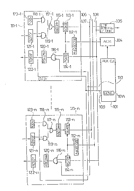
FIG. 1 sho~s a TDM sys-tem ~7hich includes a
mul-tiplex control uni-t 101 fo~ no-t only con-trolling -the
bi-t-by-bit mul-tiplexing/demultiple~ing o~' data :Ero~n the
or signals -Erom a high-speed digital ].ine bu-t al,so
sequen-tially transmittirlg~a receiving con~rol s,igrlal 11~ and
a sending control signal 109 -t;o a ~ank o~' D'rIli's l:L1-l
-~.3-
lZ~333
~through 111-n -to -thereby con-trol a sending signal switchin
circuit, ~hich ls to be described below, accordirlg to a
predetermLrled ch.~nnel bit group of in~`ormation. O-t~ler
elements 10~ through lQ~ are iderltica] wit;h those o~' li'I~ l()
ancl will not describe~ in detail.
~ ll the ~TIFs 111-1 -throug~h 111-n are~ idelltical
and only -the D'l'IF 111-1 will be described. 'l'~e ~'l'Ili' 111-1
corlsis-t;s o~ an ~cll~ECO~ llZ-1, an SG~ 113-1, a I~G~'l'E 114-1,
an SSCONY 115-1, a ~S~ONY lZ0-1, an SDI~Ili' 1~1-1, ~nd a 12~Slli'
lZ2-1, which are all identicai with -t~lose o~ FIG. 10, ancl a
N~ND ga-te 11~-1 formirlg a receiving con-trol ga-ter ancl a
sending signal s~itchlrlg circui-t consis-t;ing o~ an ~l~ irate
117-1, an ~N~ gate 11~-1, and a N~N~ L~ate 119-1, which are
provided l'or purposes o~ easier understanding o~'-the
~unc-tions o~ the serldingr sif,~nal switchirlfJ circuit. 'l'he
sending signal swi-tchin~ circui-t also has an all "1" code
generator 123-1 which is a circuit for genera-ting co~es
t~le sanle level.
The ~ul-tiplex control unit 101 has a sen~ing
control signal generator 101~ which ~enerat;es a senclin~r
con-trol signal ~'or controlling -t~le N~N~ ga-tes 116 ~nd 11~3,
and the AN~ gate 11~.
FlG. 2 shows an example o~ bi-l; set-tinL~rs of -the
sendinf,S control signal 109 an~ receivirlg control sigrlal 110.
'l'he details will 'be describe~ later herein.
llow signals are transmit-ted by respective~ s-tations,
accorcling to those se-ttinL,~s o~'-the sendingr control si~,~nE-~l
109 and receiving con-trol sigrlal 110 are illus-tra-ted in
FIGS. 5a-5d. In -this exa~ple, six channels are necessary
~or signal -transmissiorl among ~'our s-tations Ml -t~lrouf~h M4 so
_~_
~L292333
-that a ~rar~e o~ ~ bits a-t; a bl-t rate ol` 'l~ Kb/s is divi ded
in-to six 1~-bi-t or 2-octet chanllel bit groups. ~'acl-l bit
~roup is la~beled ~ith a letter ~ -through L and, i.n a ~it
group, the bit mul-tiplexing is employed. I;`or example, in
-the bi-t group ~, M1 ~ M4, in -the bit group B, Ml -~ M3, in
the bi-t group C, M1 -~ M~, and in the bit ~roup D, M2 -~ M3,
an(l so orl.
In operation, -the multiple~ control uni-t 101
sequentially ~transmits a sendirlg con-trol signal 109 and a
receivingr control signal 110 to tlle ~'l'Il~'s 111-1 l,hroul,~h
111 -Il according to a predetermine~ channel bit grou~p o~
in~ormatiorl. ~s shown in FIG. 2, eac~l s-ta-tiorl transm:it~ a
logical "O" or "1" ~or each bi-t group or chanr:~el. 'l'he
sendirlg con-trol signal 109 is se-t to a logical "0" to send
da-ta in the bi-t group and -to a logical "1" to send an all
"1" code ~hile the recei~ing con-trol signal 110 is se-t -to a
logical "O" -to inpu-t -the received signal to -the I~SCONV 120-1
through lZO-n and to a logical "1" -to inhibit the inpu-t.
'l'hese sendirlgr ~nd rccei~ing~ con-trol sigrnals are supp:Lied to
all -the DTIFs 111-1 -through 111-I1.
'l'he da-ta si~nal ~rom -the D'l'li, is sen-t -to the S~
lZ1-1 and -then the N~ND ga-te 119-1. Whell the ~dDl!.COD 117.-1
finds i-t5 own address on -the a~ress bus 10~, -the ~
113-1 and ~G~T~ 114-1 open. When the sending control signal
109 is a logical ''O", -the N~N~ ga-te 11'9-1 opens to pass t~le
da-ta signal ~rom -the S~RIF 121-1 to -the SSCONY 115-1 via the
OR ga-te 11'1-1. The bit ra-te is conver-te~ an~ the data
signal is ou-tpu-t on the sending bus 107 in -the al]o~-ted
time slot. 'rhe subse~uen~ operation i5 i~entical with -that
o~ -the conven-tional system and the descriptiorl wlll ~e
--10--
~;~92333
omi-t-ted.
When -the sending conl;rol signal 10~3 i5 a lolrical
'1'', -the AM~ gate 11~-1 opens so tha-l; arl output :Ero~n t~e all
"1" code genera-tor 123-1, WhiC~l renders a bit, in t~le time
slot -to a logical "1", is input to -the SSCONY 115--1 ior
~trarlsmission o~ a logical "1". The AdD~CO~s 11~-1 -t~lrough
112-n se~uerl-tially open while the D'~'IFs 111-1 -throu~h lll-n
in the same channel bit group ~transmi-t a logical "1" as long
as the sen~ing con-trol signcal is a logical "1". 'l'hus, an
all "1" code is ~ormed and transmit-ted.
The received signal on -the receiving bus l0~ is
inpu-t -to 't~lC NAND ga-te 11~-l via the l2(;A'l'Ii' 114-1. W~-len -I,Ile
receiving con-trol signal 110 is a logical "O`', t'he N~N~ gfcll,e
~ 1 opens to input -the received signal -to -the l~S~ONY 120-l
so that the RDSIli' 12~-1 -transmi-ts -the data sigrlal to -the
D'rE. ~len -the receiving control si~Snal 110 is a logical
"1", -the NAN~ gate 116-1 does no-t open, e~Xec-tirlg no
receivirlg; i.e., any reception is neglec-ted.
The ~ranching urli-t in this embodi~ent is composed
o~ only AN~ ga-tes so -tha-t an all "1" code is used ~'or -the
equal level code genera~tor. I~' an all "0" code i5 used, o~
course, -the all "1" code genera-tor is replaced by an all "0"
code generator.
FIG. 3 shows another embodiMent of ~the invention
Unlike the above eMbodi~ent, the mul-tiplex cont:rol uni-t 1~1
o~ this embodiment; fur-t'her inGludes a memory 1()'3 arId a
microprocessor lU2 capable of set-tin~ the sending con-trol
signal 109 and the recei~ing control signal 110 1`or each
station at each -time and e~sily changing the se-t-tin~s
FIGS. ~a-~d illus-tra-te se-t-ting patterns o~ the
3~3
sendinf~ control signal 10~ and the receivirlg~ corltrol si~rlal
11~ for each station a-t each -time pat;t,ern, in which '1`~-'1'3
are set-ting~-time pa-tterlls and (1) and (2) are ou-t;pu-t
set-tings o:f -the sending control signal 109 and t.lle receiYi
control signal ~10, respectively. '1'0 is a condi-tion under
which data signal transmission is always possible amor~ e
respec-tive sta-tiorls.
FIG. ~a shows a -time pattern in whicli all cllannel
bit ~roups be-tween the mast,er s-tatiorl Ml and t~le slave
sta-tions M2-M~ are assigned to a particular slave sta-tiorl,
;from which da-ta are collec-ted. 'l'he par-ticular slave s-tation
is changed ~ith time so that data are collected se(1~lelltial]y
from all the slave statiorls.
In FIG ~b, all the channel bit grouE~s ~mon~ the
slave stations are assi~ned to a particular slave stat~on,
~rom which da-ta are collec-ted '1'~1e particular slaYe s-tatio~
is chan~e~ with time so that da-ta are collect;ed sequentially
from all the slave s-ta-tions.
In FIG. ~c, all the chanllel bi-t groups bel;ween -the'
master sta-tion and the slave s-tation and a~orlg t~le slaYe
stations are assigned -to a particular slave sta-tion, ~rom
which da-ta are collected. 'rhe particular slave sta-tion is
changed with -time so t~lat data are co]lec-ted sequen-tially
from all the slave s-ta-tions.
In FIG. ~d, all ~the channel bi-t b~roups between the
master sta-tion an~ -the slave station and among -the 31ave
statioris are assi~ed -Lo ~e-tween a par-ticular ~lave sl,al,ior
and a Plurali-ty of master s-tations so that -the master
stations collec-t data fro~ the par-ticular slave s-tatio~l~ A-t
-the same -time, the par-ticular slave sta-tion is change(l with
-12-
2333
time so -that -the mas-ter s-ta-tions collec-t data se~uentially
~rom a:ll -the sla~e stations
FIGS. 5,~-5d illus-tra-te signals o~ -tl-le -time ~a-t-tern
T1 transmitted among the ~espec-tive s-tat,ions, with the
sending con-trol signal 109 and -the receiYing con(,rol ~iL~naL
llV se-t as shown in E`I~S. 4a-4~.
The opera-tions o~ t~le respec-tive unit~ o li'lG. 3
are the same as those o-~ FIG. 1. 'l'he ou-tpu-t se-t-ting~ o~ the
sending con-trol signal 109 an~ -the recei~ing control sigrla]
110 as shown in E'IGS. ~a-4d are storecl in -the r~emory 103 of
-the mul-tiple~ control unlt 101 in each T~M 1-~ of sta-t:ion
Ml-M4. 'l'he microprocessor lU2 controls -the me~lory 103 to
provide an ou-tpu-t a-t a time according to each se-t;-tin~ table
This allows tr~nsmission signals to ~)e processed accordint-J
to each time pa-ttern as sho~n in l~IG~. 5a-5d. 'l'}la-t is to
say, the time pa-t-tern T1 of FIG. 4a al:Lows -the signal
transmission o~ FIG. 5a, the time pa-t-~;ern 'l'1 ol' FJG. ~b
allows the ~igrrlal transmission of FrG. 5b, and the -time
pa-ttern 'l'1 ol' FIG. ~c allows -the sig~lal transmi~sioll o~ r~'L(;.
5c, and so on. In terms of the ~umber of charlrlel bit gro-lps
in the case o~ M2 -~ M1, t~e bit brroup (l)(G) at a t;in~e
pattern 'l'0 in l,he sta-tion M2 is increased -to three bi-t
groups (l)(G), (2)(H), and (3)(I) in l~'IG. ~a, two ~it groups
(l)(G) and (~)(J) in FIG. 5b, and six bit groups (l)(G)
-through (6)(L) in FlG~ 5c.
FIG. 5d shows -that at time T1 the s-tal,ion M2 is
allowed -to use -three bit groups for each of two mas-ter
s-ta-tions M1 and M4. ~lthough this is for -the time set-tin~
pat-tern T1, the s~me rules~apply -to -the time set-ting
pa-tterns '1'2 and T3, respec-ti~ely.
-13~
~L~92333
li'lG. 6 5how5 a ~OV b/s sigSnal i'~ame ~'ormat; more
specifically, li'IG. 6a sl1ows a si~nal ~`rame on a hig~1-speed
digital lirle and FIG. 6b illus-trates a multi~'rame consis-tiI1~
of ZO ~'rames MUi-R Nos. l-20. Ir1 li'IG. 6a, time slo-ts ('~'S) are
de~ined irl oc-tet urli-ts. k co~-tinuous time slot k'l'S (k x ~4
Kb/s) :~rom j to (j -~ k - l) in a ~rame lengt~1 l'l'S is
allotted -to a chanr1el indica-ting that a secluence o~' bit;s
l-~3~ is processed w.ithou-t oc-te-t divisiorl in -tl1is su~l.`rame
kTS. j, k, and l are ir1-te~Sers. When -the bi-t ra~te ol a
hi~h-speed di~i-tal line is l.536 Mb/s, l is 24. Thus, i~
the bi-t ra-te o~ in~ormation branched -to a certain char1r1el is
~2 ICI)/SJ t~1en k = ~. ~lso, l i~ 9~; ~or ~.l44 Mb/s. F o~
the subframe :is a frame synchronizing 'bit ~nd cor1stitu-tes,
~or example, the CCI'1"1' recommer1da-ti.oxl X,5() syr~chrox1izinl,J
pattern. 'l'hi5 synchronizir1~ pat-tern may be ~II10 ther ~:ie~Uel~Ce
oI- codes. ~1-D~k-1 are dat:a bi-ts for transmissior1 o~' da-ta
or con-trol sigr1als.
The mul-ti~rame o~ FIG. 6b is cornposed of Z0
sub~rames Bit No. l is an li` bi-t ~'orming -the above
synchroni~ir1g pattern. Bi-t Nos. 2-~3k in sub~rames M~ Nos.
l-20 are used to ~orm channels (~ a-t b:it No. l, ~E'1
No. l, is a pass n1onit;orin~ bit and transmil;s r1orn1al "l" a~
abnorrnal "0`' accor~ing to -t~1e ~CI'1"r reco~ er1datior1
lllG. '7 shows -the num~er o~ cha11~1els availab].e at
,various data transmiss:ion speeds dependir1b on -the nu1l~ber of
bi-ts a-t -the same bi-t No. in sub~ra~es of -the mu,L-ti.l`rame
format of l~ . 6b. I-t means tha~t a plurali-ty o~' char1rlels
may be lormed Wi't~1 bi-ts of the same bit No. at bit ra-tes o~'
l.2 Kb/s, 2.~ Kb/s, e-tc. pelow 64 Kb/s.
FIGi~ ~3 shows ar1 ~3 Kb/s si~Sr1al ~rame :Lormat; 1i`IG.
~2~2333
~a is a signal frame on a ~1igh-spee(1 digital line an(1 1~
Ub illus-trates channe~ alloca-tion ~or sig~al transm:ission a-t
bi-t ra-tes of ~ kbfs, l~i Kb/s, 32 Kb/s, and 64 Kb/s. Like
reerence numerals ir1dicate t~1e same elemer1ts as -those of
FIG. 6. I1-Io k are in~ormation bits.
When t}1e -transM:ission speed of da-t~ sigl1als is l.2
Kb/s or i-ts mul-tiples (q times), the dal;a is stored ~lorla~
wltl1-the ancillary con-trol slgnal whic.h has mul-ti~oint
sampled a-t ~00 b/s.
FIG. (i ~l1ows how a plurali-ty ol' da-ta termi~n~l
lines at bit r~tes of l.Z Kb/s -to l9.Z K~/s are allot-ted in
n multiPrame. E'or -the ~00 b/s signals, char1r1els are rllade 1n
bit rate units oP (q ~ l.2 Kb~s -1- m ~ ~OU b/s) where m is
the nwnber o~ control signals, and allo-l;ted in the above
multilr~me ~`ro~n thc beginning.
Il' q = l and m - l, -then tl1e bi-t ratc is l.G Kb/s,
-thus requiring 4 bits in the mul-tiframe Consequex1-tly, Por
lO data terminal lines at l.2 Kb/s, bi-t No. 2 acco~1odal;es
CHl-CE15 and bi-t No. 3 accomllloda-tes C~16-~1lO includin~
con-trol sigr1als~ Similarly, if q -- 2 and m = l, -then the
bi-t rate is 2.~ Kb/s, requirin@ 7 bi-ts :iIl the mU.I.ti~'rallle.
Consequen-tly, for ~iYe data terminal lines of ~.~ 1Cb/s, bi-t
No. ~ accommoda-tes ~Hll through part of ~1-113 and bi-t No. 5
accommodates -the res-t of CHl3 throug}1 C1115 includin~ control
signals. Similarly, if q = 4 and m = l, -then tt1e bit rate
is 5.2 Kb/s, requiring 13 bits in t;he multiframe.
Consequently, ~'or -three data i-tems oi` ~.~ Kb/s, C11 21, C~122
and C1-123 are alloca-ted to bit No. 6, bit No. ~i a~1d pa-rt of`
bi-t No. 7, and the rest o~' bi-t No. '1, :res~)ect:ively. '1'he
char1nel numbers are ~iver1 on -the basis oi' data bi-t rat;es a11d
-15-
333
no-t con-tirluous from ~I-Il. At ~ = U an~l m = 1, the ~il; rate
is lO.2 Kb/s, and C1131 an~ CL-132 are allotted to bi-t ~o. ~
arld p~rt of bi-t. No. 9, and the rest o~ bi-t No. 9 ~n~ ~:i-t No.
10 J repectively. Wherl-the bi-t rate i5 1~ . 4 or 19.2 Kbts,
pluraL bits in a subframe are ~is-tribu-ted in -the multirame
for allocation. ~n example ol' the rlumber o~ charlrlels
a~ailable in a mul-tiframe consis-tirlg of 20 subrames is
s'hown in FIG. 7.
l~or bi-ts Nos . higher than bit No. l6, no
illustra-tion is provided bu-t i-t is apparen-t -tha-~ -the
multifrarne is used in the s~le way or plural bits in a
sub~'rame are used -to transmit hlgh-speed ~a-ta si.grlal~ o:E ~,
16, 32 J or 6~ Kbfs.
In -the multiframe i'ormat of FI~'. 6b, ~L13Z i~.
alloca-ted -to -the bit No. lU while the MF~ Nos. ll-~0 ~re
blank, -to which data charmels o~' other bit r~tes May be
allocated for achie~ing higher effic:iency. For example, the
allocation of data channels of ~..4 Kbfs increclses -the
mul-tiplexing efficiency.
FIG. 9 shows the irame i`ormat oi a telephorle
signaling signal. Signaling is clccomplished by allocatirlr
data, which has been mul-tipoint sampled at mul-tiples oi' ~0~
b/s (400 and ~00 b/s in -this e~ample) for each chanrlel, to a
single bit No. in -the rr~ltiframe for transmission. For -l;he
-transmission of a signaling signal, the same mul-tiirame
synchronizin~ pa-t-tern as -that oi' FIG. 6 is use(1 l~owever,
-the synchronizirlg pa-t-tern may be another se~uence ol' bi-ts.
Data oi' no more -than 6~ Kb~s, signals o~ 8 Kbf '-3, and
signaling signals may be m~l-tiplexed in a single subfr~ne.
When no branching ser~ices are required~ the Ml1ltii'rame
~Z333
synchroni~ing bit of a pluraLit~ of subframes ~ay be
allocated to a single subframe and other subXrames are
processed in the same multiframe phase, thus eliminating the
need for the other multiframe synchronizing bits.
l`he number of subframes constituting a multiframe
has been 20 in the aboYe embodiment but, of course. it is
not limited to this number. Where signals of Lo~ speed are
transmitted, more than 20 frames, for example, 80 frames ma~
be used to form a multiframe. In such a case, t~e minimum
multiplexing speed is 100 b/s. 0~ course, t~e present
'; ,- invention is applicable to digital lines of higher speeds
such as 2.048 or 8.192 ~b/s or e~en 32 Mb/s.
''' ' .
. . .
.
,