Note: Descriptions are shown in the official language in which they were submitted.
1~2777
COMB FILTER PRESSU~E/TEMPERATURE SENSING SYSTEM
1 BACKGROUND OF ~HE INVENTION
The disclosed invention generally relates to sensing
systems, and is more particularly directed to a sensing
system having passive elements in its transducer.
Sensing systems may be utilized in applications
where one or more parameters (e.g., pressure or tempera-
ture) is sensed at a location that is remote from the
readout device. For example, pressure and temperature
sensing systems are utilized in oil and gas wells to
provide pressure and temperature information, sometimes
sensed at the well-head and/or down-hole. Such sensing
systems may be utilized to optimize production efficiency,
and to determine operating parameters that are useful in
assessing the well's performance status.
Known pressure and/or preCsure sensing systems, such
as those used in oil wells, typically include active
devices (e.g., transistors) in the transducer and its
associated components. In oil well applications, the
transducer (i.e., the sensing element for sensing pressure
or temperature) is sometimes located down-hole, and is
therefore subjected to a very harsh environment. Down-
hole transducers that utilize active devices generally
have limited lifetimes due to`the harsh environment, and
moreover are very difficult and costly to replace. As a
result, they typically do not get replaced, and the oil
wells are operated without the benefit of pressure and
temperature information.
PD 86301 361/P10
sZ~777
1 A further consideration with known sensing systems
that utilize active devices in their transducers and which
are utilized in a harsh environment is drift. Such
consideration is particularly important in applications
such as oil wells where access to the transducers is
difficult and costly after installation.
A further consideration with known pressure or
temperature sensing systems having transducers that
utilize active devices is the necessity of providing power
to the active devices. In the case where the transducer
is placed down down-hole, the power must be supplied
down-hole, thus posing another possible failure mode
through breakage of the power-supplying electrical conduc-
tors, or poor contact in their electrical connectors.
SUMMARY OF THE INVENTION
It would therefore be an advantage to provide a
pressure or temperature sensing system which functions
reliably for extended lifetimes in a harsh environment.
Another advantage would be to provide a pressure or
temperature sensing system which provides for long term
accuracy.
It would also be an advantage to provide a pressure
or temperature sensing system that utilizes only passive
devices in its transducer, and which does not require
electrical power for operation of the sensing element in
the transducer, or for relay of sensed data from the
transducer.
An aspect of the invention is as follows:
.
lZ~?Z777
An sensing system comprising:
means for providing optical illumination having
a bandwidth of at least 25 nanometers;
means for transmitting said optical illumina-
tion;
transducer means responsive to said transmitted
optical illumination for amplitude modulating said
transmitted optical illumination as a function of a
monitored physical parameter to provide an amplitude
modulated optical illumination having generally
sinusoidally varying nulls across the spectrum
thereof, the frequency of said nulls varying across
the spectrum of said modulated optical illumination
and being a function of the monitored physical
parameter;
means for transmitting said modulated optical
illumination;
means for spectrally dispersing said transmit-
ted modulated optical illumination to provide a
spectrally dispersed optical signal indicative of
the spectral content and amplitudes of said modulat-
ed optical illumination;
means responsive to said spectrally dispersed
optical signal for extracting the frequency varia-
tion of said periodic nulls to an electrical signal
indicative of the substantially constant frequency
of said periodic nulls across the spectrum of said
modulated optical illumination;
means for narrowband filtering said electrical
signal to provide a filtered signal; and
means responsive to said filtered signal for
providing an output signal indicative to the sub-
stantially constant frequency of said periodic
nulls.
12~Z7~7
2b
By way of added explanation, the foregoing and other
advantages are provided by a sensing system which includes
a wideband optical source for providing optical
illumination having a bandwidth of at least 25 nanometers,
and an optical fiber cable for transmitting the optical
illumination to a remote location. A transducer responsive
to the transmitted optical illumination amplitude modulates
the transmitted optical illumination as a function of a
monitored physical
lZ~27~77
1 parameter to provide an amplitude modulated optical
illumination having generally sinusoidally varying nulls
across the spectrum thereof, the frequency of the nulls
varying across the spectrum of the modulated optical
illumination and being a function of the monitored phys-
ical parameter. The fiber optic cable (or another fiber
optic cable, depending on the transducer implementation)
transmits the modulated optical illumination to an optical
spectral analyzer which provides a spectrally dispersed
optical signal indicative of the spectral content and
amplitudes of the modulated optical illumination. A
clocked detector array responsive to the spectrally
dispersed optical signal is clocked at a varying clock
rate to remove the frequency variation of the periodic
nulls across the optical spectrum, so as to provide an
electrical signal having a substantially constant fre-
quency of the nulls. Narrowband filtering circuitry
filters the electrical signal of substantially constant
frequency to provide a filtered signal, and output cir-
cuitry responsive to the filtered signal provides an
output signal indicative to the substantially constant
frequency of the periodic nulls.
BRIEF DESCRIPTION OF THE DRAWING
The advantages and features of the disclosed inven-
tion will readily be appreciated by persons skilled in the
art from the following detailed description when read in
conjunction with the drawing wherein:
FIG. 1 is a block diagram of a pressure sensing
system implemented with a Michelson interferometer.
FIG. 2 is a block diagram of a pressure sensing
system as alternatively implemented with a Mach Zehndar
interferometer.
PD 86301 361/P10
Z~*7
Figure 3 is an overall timing sequence diagram for
the analyzer of the invention.
Figure 4 is a block diagram of one embodiment of
the invention.
Figure 5 is a detailed timing sequence for the Fast
Fourier Transform transform analyzer.
Figure 6 is a block diagram of an alternate
tracking filter analyzer embodiment of the signal
analyzer.
Figure 7 is a detailed timing sequence diagram for
the tracking filter processor of the invention.
Z7';7
1 DETAILED DESCRIPTION
In the following detailed description and in the
several figures of the drawing, like elements are iden-
tified with like reference numerals.
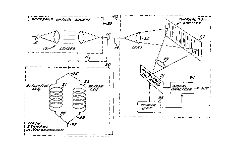
S Referring now to FIG. 1, shown therein is a pressure
transducing system 10 in accordance with the invention and
which includes a wideband optical module 20 for providing
point source illumination for a fiber optic cable 11. By
way of example, the wideband optical module 20 can provide
illumination having infrared (IR) wavelengths, near IR
wavelengths, or visible light wavelengths. The fiber
optic cable 11 is coupled to a transducer 30 which ampli-
tude modulates the source illumination provided by the
fiber optic cable 11 by placing periodic nulls across the
spectrum thereof. The modulated illumination is provided
to an analyzer 40 via the fiber optic cable 11 and the
fiber optic cable 13.
By way of example, in an oil well application the
wideband optical module 20 might be located at the well-
head, or in the case of sub-sea wells at a shore-based
station, or at a sub-sea flow control assembly at the
well-head. The transducer 30 would be positioned down-
hole in the oil well, while the optical analyzer 40 would,
for example, be surface-based, such as at a monitoring
station or at a well control station.
The wideband optical module 20 includes a wideband
optical source 15, which by way of example may be one or
more high brightness wideband light emitting diodes
(LED's). A collimating and focusing lens system 17
optically couples the output of the wideband optical
source 15 to the fiber optic cable 11 via an optical fiber
12 and a three-port optical splitter/combiner 36. Alter-
natively, the output of the wideband optical source (or
sources) is directly coupled to the optical fiber 12.
PD 86301 361tP10
lZ~tZ7~7
1 The wideband optical source 15 should provide a
bandwidth commensurate with the requirements for the
pressure range and accuracy of the transducer 30. By way
of example, such bandwidth may be 20 to 80 nanometers with
the center of the bandwidth being at, for example, 850
nanometers; i.e., an IR optical source having a bandwidth
of about 2 to 10 percent.
As an alternative to a single wideband optical
source such as an LED, the wideband optical source 15 can
include a plurality of optical sources, such as LED's,
which may be combined to increase the total optical power
and/or to cover respective portions of the desired optical
spectrum. The outputs of such optical sources would be
combined, for example, with fiber optic combiners.
A further alternative for implementation of the
wideband optical source 15 would be a laser diode that is
capable of being swept over the required wavelength range.
The use of such a wavelength-swept source requires either
that the source be capable of covering the bandwidth of
interest without wavelength gaps, or its modes must be
spaced considerably closer in the wavelength domain than
the minimum spacing of the periodic interferometeric nulls
created by the interferometer in the transducer 30.
As discussed more fully herein, the transducer 30 is
implemented with one of several types of interferometers
that are capable of creating amplitude modulation in the
form of periodic peaks and nulls across the illumination
spectrum provided by the optical source 15, where the
periodic peaks and nulls are approximately sinusoidal in
shape. One such type is a Michelson interferometer as
shown in F~G. l; another ~s a Mach Zehndar interferometer
as shown in FIG. 2.
As another alternative optical source, an incandes-
cent infrared source can be utilized as the wideband
PD 86301 361/P10
l~Z7 77
1 optical source 15, provided that sufficient light can be
coupled into the fiber optic cable 11.
In the example embodiment shown in FIG. 1, the
transducer 30 includes a Michelson interferometer which
more particularly includes first and second optical legs
21, 23 comprising respective optical fiber channels that
are optically coupled via a three-port optical splitter/-
combiner 35 to receive the illumination provided by the
fiber optic cable 11 which receives the source illumina-
tion via the three-port optical splitter/combiner 36.
The three-port optical splitter/combiner 36 allows
light to pass from the wideband source down the fiber
optic cable 11 to the down-hole transducer 30 while
permitting light returning from the down-hole transducer
30 to be extracted into another optical fiber channel 13.
Such an optical splitter/combiner is known in the art and
provides negligible internal cross-coupling between its
input from the LED source and the output optical fiber
that extracts the return light from the interferometer.
The three-port optical splitter/combiner 35 func-
tions similarly to the optical splitter/combiner 36.
The first optical leg 21 of the interferometer is a
reference leg which does not change significantly in
length with change in the pressure being sensed, while the
second optical leg 23 is a sensor leg which changes in
length with change in the pressure being sensed. The ends
of the optical fibers comprising the first and second
optical legs 21, 23 are made highly reflective so that the
light in each leg of the interferometer is returned along
the legs and combined in the three-port optical splitter/-
combiner 35 so that the now combined reflected light
returns via the fiber optic cable 11. The combined output
illumination from the Michelson interferometer, after
having been amplitude modulated across its spectrum by the
PD 86301 361/P10
lZ~Z777
- 1action of the interferometer, is provided to the analyzer
40 via the three-port optical splitter/combiner 36.
As an alternative to the Michelson interferometer
shown in FIG. 1, a Mach Zehndar interferometer can be used
as shown in FIG. 2. In such embodiment, the illumination
transmitted by the two legs 37, 38 of the interferometer
is combined in a three-port optical splitter/combiner 39
for transmission to the analyzer 40 via a return fiber
optic cable 14.
10Referring again to the Michelson interferometer
implementation of FIG. 1, the first and second optical
legs 21, 23 can comprise, for example, respective single
mode optical fibers. The optical fiber of the reference
leg 21 is wound in a coil or otherwise configured in the
transducer 30 so that its length does not change signifi-
cantly with pressure. The optical fiber of the sensing
leg 23 is wound, for example, on an expansible cylinder,
and configured in such a way that the diameter of the
cylinder increases by a small amount in proportion to
pressure, thereby increasing the length of the sensor leg
23. An alternative to winding the reference and/or
sensing optical fiber on a cylinder is to configure the
interferometer so that the sensing optical fiber is
linearly stretched pursuant to pressure such as with a
bellows structure whose length varies with pressure. The
optical fiber of the pressure sensing leg 23 might, for
example, be made longer than the optical fiber of the
reference leg 21, whereby when pressure is increased, the
length of the sensing leg 23 increases even more with
respect to the reference leg 21. By way of more specific
example, the differential length at the minimum atmos-
pheric pressure to be encountered might be 0.01 inches
when not subject to down-hole well pressure. Under
maximum pressure, the differential length might increase
to 0.11 inches.
PD 86301 361/PlO
12~Z7 ~7
- 1 Apart from the slightly longer length in the sensing
leg 23, the optical legs 21, 23 have relatively long equal
lengths. The relatively long length in the sensing leg 23
provides for an easily sensed amount of elongation as a
function of pressure without incurring permanent fiber
deformation or breakage. The sensing leg 23 is made of
nearly equal but slightly longer length than the reference
leg, so that the two legs never become equal at any
pressure within the range to be sensed. However, at
maximum pressure (maximum differential lengths in the
interferometer legs), the periodic nulls across the
spectrum must not be too closely spaced to be resolved in
the analyzer 40. At the same time, the number of nulls at
maximum pressure must be sufficiently large that the
change in null spacing can be discriminated with suffi-
cient accuracy to provide the required pressure accuracy.
As an example of lengths for the two optical legs
21, 23, of the Michelson interferometer shown in FIG. 1,
the reference leg might have a length of 100 inches, while
at nominal atmospheric pressure the sensing leg might have
a length 0.01 inches longer (i.e., 100.01 inches). At
maximum pressure to be sensed, the sensing leg 23 might
increase in length by an additional 0.1 inches (to
100.11). Thus, 0.01 inches of differential length might
correspond to nominal atmospheric pressure, while 0.11
inches of differential length might correspond to 5000
pounds pressure. Since the illumination is reflected back
along both legs 21, 23 of the Michelson interferometer,
the effective differential length between the two legs and
the effective change in differential length with pressure
is doubled,
The Michelson interferometer of FIG. 1 can be
alternatively implemented with optical paths in air
instead of optical paths in optical fibers. With such
implementation, the physical parameter being monitored
PD 86301 361/P10
~2~
1 (e.g., pressure) would affect one optical path in air
instead of elongating an optical fiber~ Such an alterna-
tive implementation might include an optical splitter for
splitting the optical illumination provided by the fiber
optic cable 11 into two optical channels~ One channel
would comprise the reference channel which has a substan-
tially constant optical path. The other channel would
comprise the sensing channel and could include a first
lens system to collimate the optical illumination received
by such channel and a movable mirror to reflect the
collimated optical illumination. The reference channel o~
the interferometer can comprise an optical fiber having a
highly reflective end, with a length to provide an optical
path that is slightly shorter than the optical path of the
lS sensing leg. The movable mirror in the sensing leg o~ the
interferometer is adapted to vary its distance from the
source of the illumination for sensing channel as a
function of the physical parameter being monitored. The
combined light returned from the interferometer is then
provided to the analyzer 40 via the fiber optic cable 11
and the three-port optical splitter/combiner 35.
For ease of later understanding, it should be
pointed out that the differential length between the
reference leg 21 and the sensing leg 23 of the Michelson
interferometer shown in FIG. 1 creates periodic generally
sinusoidally varying interferometric nulls across the
spectrum of the combined illumination relayed by the fiber
optic cable 11 to the analyzer 40. Similarly, the differ-
ential length between the legs 37, 38 in the Mach Zehndar
interferometer shown in FIG. ~ creates generally sinusoid-
ally varying periodic nulls across the spectrum of thecombined illumination relayed by the fiber optic cable 14
to the analyzer 40.
The spacings of the periodic nulls across the
spectrum created by the action of the interferometer is
PD 86301 361/P10
zt;;~7~7
1 deter~ined by the differential length between the two legs
of the interferometer and the wavelength, and is thus a
direct measure of pressure. However, as will be discussed
in the paragraphs to follow, the cycle-to-cycle spacing of
these interferometric nulls across the spectrum as imaged
onto a photodiode array 31 is not uniform; instead they
vary inversely with wavelength across the wideband spec-
trum provided by the wideband optical source 20. That
frequency-varying component must be removed from the
photodiode serial readout before narrowband filtering the
data to improve the signal-to-noise ratio and to more
precisely determine the frequency of the periodic nulls.
Once this frequency-varying chirp-like component has heen
removed, the analyzer 4Q functions to determine the
frequency of the constant-frequency burst, thereby provid-
ing a direct indication of the pressure sensed by the
sensing leg of the interferometer (leg 23 of the Michelson
interferom~ter in FIG. 1 and leg 38 of the Mach Zehndar
interferometer in FIG. 2).
2Q More particularly, the analyzer 40 (FIGS. 1 and 2)
performs three overall functions: (a) it optically spec-
trally analyzes the optical output of the interferometer
and images the resulting spectrum onto a photodiode line
array; (b) it converts the optical spectral analysis into
an electrical signal by serially reading out the photo-
diode array with a frequency-varying readout clock rate
(the action of the frequency-varying clock rate is to
provide a serial output from the photodiode array that is
essentially a constant frequency burst); and (c) it
performs narrowband filtering and frequency determination
of the serial readout from the photodiode array 31. The
narrowband filtering achieves a significant improvement in
signal-to-noise ratio. On the basis of the eleckrical
spectral analysis of the readout data, an output is
PD 86301 361/P10
-`` 12~t2777
1 provided that is a direct measure of frequency of the
readout burst, i.e., a direct measure of sensed pressure.
In a preferred embodiment of the analyzer 40, the
frequency determination of the electrical signal read out
from the optical detector array is performed by spectral
analyses in a Fast Fourier Transform processor which, in
effect, provides a bank of closely and contiguously spaced
filters whose outputs are sampled at the end of each
essentially constant frequency readout burst from the
optical detector array which can be a photodiode line
array or a charge coupled device (CCD) line array.
Interpolation between the relative magnitudes of the
filter outputs can be performed to improve the resolution
of the system over that provided directly by the number of
filter channels.
The analyzer 40 includes a collimating lens 25 which
collimates the illumination provided by the transducer 30.
Particularly, in the Michelson interferometer embodiment
of FIG. 1, such illumination is provided to the analyzer
40 by the optical fiber 13 which is coupled to the three-
port optical splitter/combiner 36, while in the Mach
Zehndar interferometer embodiment of FIG. 2, such illu-
mination is provided to the analyzer 40 by the fiber optic
cable 14.
The collimated illumination provided by the colli-
mating lens 25 illuminates a diffraction grating 27, which
in its simplest form includes rulings that are equally
spaced at, for example 1200 lines per millimeter. The
diffracted spectrally dispersed illumination outputted
from the diffraction grating 27 is focused by a lens
system 29 onto a detector line array 31 which by way of
example may be a photodiode line array or a CCD line
array.
The differential length introduced between the two
legs of the interferometer creates periodic peaks and
PD 86301 361/P10
1Z~;277-7
12
l nulls across the spectrum of the wideband optical source,
and such nulls are imaged across the photodiode array 31
by virtue of the spectral analysis action of the diffrac-
tion grating 27. However, these periodic nulls are not
exactly equally spaced across the spectrum of the wideband
source. As a result, if no correction were made, the data
as serially read out from the photodiode array would
contain a chirp-like (time varying) frequency component.
This chirp-like component must be removed prior to narrow-
band filtering.
The existence of the non-linear spacing of the nulls
across the spectrum of the wideband optical source 20 can
be shown by the following expression for the relative
phase Fe between the two legs of the interferometer, where
Delta is the differential length between the two legs of
the interferometer and lambda is optical wavelength. It
should be appreciated that in the case of the Michelson
interferometer (FIG. 1), Delta is the two-way differential
length since the illumination is reflected back along the
two legs of the interferometer. That relative phase
(i.e., the optical phase angle Fe between the light
vectors in the two legs of the interferometer) is shown by
the expression below.
Fe = 2 Pi Delta
lambda
From the above expression, it is evident that the
relative phase Fe does not vary in direct proportion to
optical wavelength lambda. Since the angular spread of
the optical spectrum as imaged onto the photodiode array
is relatively small (less than 6 degrees in a typical
system), the deflection across the photodiode array 31
resulting from the action of the diffraction grating is
approximately proportional to the wavelength lambda. But,
PD 86301 361/P10
lZ~Z77
1 as shown in the expression above, the phase of the inter-
ferometric null Fe varies as 1/lambda. Thus, the phase of
the interferometric nulls varies approximately as the
reciprocal of the deflection distance along the photodiode
array.
It can be shown that this hyperbolic spacing of the
nulls corresponds approximately to the change in period of
a waveform having a linear (chirp-like) frequency compo-
nent. This varying frequency component can be removed
from the serial data electrically outputted from the
photodiode array by varying the readout clocking rate at a
corresponding linearly varying rate. Qualitatively, when
the interferometric nulls that are close together are read
out, the clocking rate is made slow, and correspondingly,
when the interferometric nulls that are more widely spaced
are read out, the clocking rate is made more rapid. The
end result of such non-linear clocking of the photodiode
array readout is that the data as read out from the
photodiode array is essentially a constant-frequency
burst; i.e., it is essentially de-chirped. The frequency
of that burst is proportional to the differential length
of the interferometer, i.e., the frequency of the burst
(as read out with a linearly varying frequency clocking
frequency) is essentially proportional to pressure.
Following the removal of the frequency varying
(chirp-like) characteristic from the data readout from the
photodiode array 31, the de-chirped readout data is
electronically processed in a signal analyzer 34. As
discussed in greater detail further herein, such signal
analysis includes narrowband filtering the de-chirped
readout data, followed by further electrical processing to
determine the frequency of the interferometric nulls
created by the differential length in the interferometer
legs.
PD 86301 361/P10
12~Z7 ~7
14
1 The timing functions for the analyzer 40 are pro-
vided by a timing unit 33 identified in FIGS. 1 and 2.
The timing unit 33 provides a clocking signal for the
readout of the photodiode line array 31. Such clocking
signal has a linearly modulated (FM'd) clock rate (i.e., a
clock rate having a linearly varying frequency) to achieve
the de-chirping function discussed above relative to the
readout of the photodiode line array 31. As discussed
more fully below, the timing unit 33 further functions to
time functions in the signal analyzer 34.
The overall timing sequence for the analyzer 40 is
shown in FIG. 3, and includes a photodiode readout inter-
val, followed by a processing interval. FIG. 3 schemat-
ically shows the FM'ed readout clock pulses discussed
above relative to de-chirping. More specific aspects of
the timing sequence will depend upon the implementation of
the signal analyzer 34 which will now be discussed in more
detail.
Referring now to FIG. 4, shown therein is a block
diagram of one embodiment of the signal analyzer 34. The
signal analyzer includes an analog-to-digital converter, a
Fast Fourier Transform filter bank, and a filter peak
selector, which together perform the signal narrow-banding
and frequency determination functions.
More specifically, the de-chirped data read out from
the photodiode line array 31 is provided to an analog-
to-digital converter 39 which provides digitized data to a
Fast Fourier Transform filter bank 40. The filters
comprising the Fast Fourier Transform filter bank 40
partially overlap one another in the frequency domain (for
example, at the -3dB points) and cover the frequency
interval that corresponds to the pressure extremes to be
encountered. Depending upon the pressure, the de-chirped
burst (essentially constant frequency) as read out from
the photodiode line array 31 will fall within the response
PD 86301 361/P10
1~2t7'~7
1 of one (or possibly two) of the filters comprising the
Fast Fourier Transform filter bank 40.
The Fast Fourier Transform filter bank provides two
important functions; namely, narrowband filtering of the
data and providing an output indicative of the frequency
of the de-chirped data burst as read out from the photo-
diode line array 31. Such frequency, after de-chirping,
is proportional to the sensed pressure.
Since the readout from the photodiode line array 31
is essentially a constant frequency burst by virtue of the
non-linear read out clocking, the resulting serial data
burst as read out from the photodiode line array 31 has a
spectral width determined by the reciprocal of the data
burst duration, and a frequency determined by the sensed
pressure.
The narrowband filtering provides for greatly
improved signal-to-noise ratio than with other techniques
for determining frequency of the data burst, such as, for
example, cycle counting. The Fast Fourier Transform
filter bank 40 performs this narrowband filtering in a
bank of narrowband filters. Depending upon the frequency
of the data burst, the signal is integrated in one of the
filters, or possibly in two of the filters if the data
burst frequency falls between the peak frequency responses
of two spectrally adjacent filters. However, the wideband
noise components that would otherwise compete with the
desired signal are reduced to only those noise frequency
components falling within the passband of the one or two
filters containing the de-chirped data as readout from the
photodiode line array 31.
If the sensed pressure is such that the de-chirped
readout signal falls, for example, at the peak response
frequency of one of the narrowband filters of the Fast
Fourier Transform transfilter bank 40, then the data burst
PD 86301 36ltP10
1~277~
1 signal in that filter competes only with the noise falling
within such filter's passband.
An example of one of the wideband electrical noise
contributors that is significantly reduced by the narrow-
band filtering process is the random noise produced bydark current in the photodiode line array 31. A further
example of wideband noise that is significantly reduced is
the noise generated in the amplifier (not specifically
shown) that would normally be used following the photo-
diode array line array 31. Still another example of acontributor of wideband electrical noise is non-periodic
spatial noise (pattern) in the photodiode line array 31.
Such noise can arise from random diode-to-diode non-equal
photosensitivity between photodiodes of the array 31.
The primary output (i.e., the filter output of
greatest amplitude) of the Fast Fourier Transform filter
bank 40 provides an indication of the frequency location
of the de-chirped data within the spectral coverage of the
filter bank 40. However, assuming the narrowband filter-
ing results in a sufficiently high signal-to-noise ratio,
the outputs of the filter bank 40 can be interpolated to
provide a determination of frequency that is finer than
the frequency spacings of the filters of the filter bank
40.
The process of determining the filter containing the
peak response to the line array readout data is performed
by the filter peak selector 41. Peak selection techniques
are well known in the art, and the present invention
contemplates commutation through the outputs of the filter
bank 40 at the end of each data processing cycle to
- identify that filter providing the output of greatest
amplitude.
The filter peak selector 41 can also be adapted to
provide an interpolated output showing where the readout
PD 86301 361/P10
.
2 7 ~ 7
17
1 de-chirped data burst lies in frequency with respect to
the response peaks of two spectrally adjacent filters.
After each filter peak selection/identification
process is completed, the data in the Fast Fourier Trans-
form processor 40 is "dumped" in preparation for reception
of the next readout data to be processed.
The detailed timing sequence for the Fast Fourier
Transforn transform analyzer implementation is shown in
FIG. 5. As shown, analog-to-digital conversion takes
place during the read out interval, such read out interval
being illustrated in more detail in FIG. 3 with FM'ed
readout clock pulses. Subsequent to the analog-to-digital
data conversion process, the Fast Fourier Transform
filtering is performed. Following this step in the
process, the filter peak selection process is provided by
the filter peak selector 41, and an output signal indica-
tive of the data burst frequency is outputted. Such
output signal is indicative of the pressure sensed.
Finally, the processing interval is completed by dumping
all data in preparation for the next processing cycle.
A quantitative example of the operation of the pres-
sure sensing system implemented with a Michelson inter-
ferometer (FIG. 1) may be helpful in appreciating its
advantages. The previously discussed example of an
interferometer differential length of 0.01 inches at
atmospheric pressure and a 0.11 inch differential length
at 5000 psi is appropriate. Since the illumination is
reflected back along both legs of a Michelson interfero-
meter, the effective differential lengths are respectively
0.02 and 0.22 inches. For an optical spectral width from
the wideband optical source 20 of 50 nanometers centered
at 850 nanometers, (recognizing that the propagation speed
of light in the fiber is approximately 0.7 of that in a
vacuum), a two-way differential length of 0.02 inches
between the legs of the interferometer includes 870.7
PD 86301 361/P10
lZ~27~7
18
l cycles at 825 nanometers, and 820.9 cycles at 875 nano-
meters. If the 50 nanometer spectrum is analyzed, there
would appear (870.7 - 820.9 cycles) = 49.8 nulls across
the 50 nm spectrum. -If the pressure were increased to
5000 psi, the two-way differential length of 0.22 inches
includes 9577.5 cycles at 825 nanometers, and 9030.2
cycles at 875 nanometers. Analyzing the 50 nm spectrum
would provide 547.3 nulls.
If these 547.3 interferometric nulls corresponding
to 5000 psi are read out in 0.1 seconds, the data burst
output from the photodiode array would have a nominal
frequency of 5473 Hz. If the transducer were at atmos-
pheric pressure, the 49.8 nulls across the spectrum would
have a nominal frequency of 498 Hz. However, as mentioned
earlier, these nulls are not equally spaced and instead
have a chirp-like spacing that can be removed by non-
linearly clocking the photodiode array readout.
After de-chirping, the resulting data burst as read
out from the photodiode array has a bandwidth approxi-
mately equal to the reciprocal of the readout time. Thus,
with a readout interval of 0.1 seconds, the bandwidth of
the data burst is approximately 10 Hz. Thus, when 5000
psi pressure is being sensed, the aforementioned nominal
readout frequency of 5473 Hz can be resolved to about 10
hertz out of 5473 Hz, i.e., 0.18%. However, if the
signal-to-noise ratio of the readout is high, the data can
be interpolated to finer accuracy.
Referring now to FIG. 6, shown therein is a block
diagram of an alternative tracking filter analyzer imple-
mentation of the signal analyzer 34 (FIGS. 1 and 2). This
alternative implementation utilizes tracking filters to
perform the narrowband filtering and frequency determina-
tion functions. The readout from the photodiode line
array 31 is provided in parallel to two switched capacitor
filters 45, 46. Switched capacitor filters are known in
PD 86301 361/P10
l~Z777
19
1 the art and are available commercially in integrated
circuit form. In a narrowband filtering configuration, a
switched capacitor filter provides a narrowband frequency
response similar to that of a parallel-tuned inductance/-
capacitor filter. The response frequency of a switchedcapacitor filter is precisely determined by a clock
frequency applied to its clock input, where the clock
frequency determines the center frequency of the filter
response. Depending on the switched capacitor filter
integrated circuit terminal wiring selection, the clock
frequency would be a multiple of about 25 to 75 times the
peak frequency response of the filter. Thus, variation of
the clock frequency provides a mechanism for precisely
tuning the response of the switched capacitor filter over
a wide frequency range.
Referring again to FIG. 6, the output of a voltage
controlled oscillator clock 42 is provided in parallel to
two single sideband modulators 43, 44. The output of a
frequency offset oscillator 47 is also provided in paral-
lel to the single sideband modulators 43, 44. The fre-
quency of the voltage controlled oscillator 42 is con-
trolled by a feedback loop as described further herein.
The outputs of the single sideband modulators 43, 44 are
respectively coupled to the clock inputs of the switched
capacitor filters 45, 46.
The function of the frequency offset oscillator 47
in conjunction with the single sideband modulators 43, 44
is to provide respective signals that are slightly offset
in frequency from the output of the voltage controlled
oscillator 42. The frequency offset provided by the
single sideband modulator 44 are positive, while the
frequency offset of the single sideband modulator 43 is
negative. Thus, the switched capacitor filters 45, 46 are
tuned at slightly different frequencies, with their
PD 86301 361/PlO
Z777
- 1 response peaks offset by an amount about equal to their
-3dB bandwidths.
The example practical values discussed further
herein for the responses of the switched capacitor filters
45, 46 and corresponding voltage controlled and offset
oscillator frequencies are based on the following consid-
erations. For example, if the transducer 30 (FIGS. 1) is
monitoring 5000 lbs. of pressure, there might be 547.3
cycles across a 50 nanometer spectrum as provided by the
wideband optical source 20. If those wideband optical
547.3 interferometric nulls are read out in 0.1 seconds,
the de-chirped data burst provided to the switched capa-
citor filters 45, 46 would be at 5473 Hz. However, if the
sensed pressure were, for example, 50 lbs., the two-way
differential length would be 0.022 inches, and correspond-
ing de-chirped readout would have a frequency of approxi-
mately 547 Hz.
Assuming that the switched capacitor filters 45, 46
are configured so that their frequency response peak is at
1/50 of the clock frequency, the corresponding frequency
of the voltage controlled oscillator 42 to respond to 5000
lbs. pressure (a nominal 5,473 Hz readout frequency) would
50 times 5,473, which is equal to 273,650 Hz. To respond
to 50 lbs. pressure (a 547 Hz readout frequency), the
required frequency of the voltage controlled oscillator 42
would be 27,350 Hz.
In order to symmetrically displace the peak fre-
quency responses of the switched capacitor filters 45, 46
by, for example +5 Hz about the de-chirped photodiode line
array readout, the offset oscillator 47 would offset the
frequency of the voltage controlled oscillator 42 by about
50 x i5 Hz, i.e., +250 Hz. in the single sideband modula-
tors 43, 44. This +250 Hz offset in the clocking rates of
the switched capacitor filters 45, 46 will result in the
their peak frequency responses to be offset by +5 Hz
PD 86301 361/P10
1~92777
1 around the frequency of the de-chirped data burst readout
from the photodiode line array 31.
The two clock inputs to the switched capacitor
filters 45, 46 are offset slightly so that, due to closed
loop feedback discussed further herein, the response peaks
of the switched capacitor filters 45, 46 will symmetric-
ally bracket the frequency of the data burst readout from
the photodiode line array 31. When the switched capacitor
filters 45, 46 are so tuned, their response amplitudes
will be alike. However, if the data burst readout lies
closer to the response peak of one of the switched capa-
citor filters 45, 46, its envelope detected output will be
greater. Thus, an error (control) signal can be derived
that can serve, in a feedback circuit, to maintain the
response of the switched capacitor filters 45, 46 symmet-
rically around the frequency of the incoming data burst
readout from the photodiode line array 31.
The feedback error signal for controlling the
voltage controlled oscillator clock 42 is derived as
follows. The output of the switched capacitor filter 45
is applied to an envelope detector 48, while the output of
the switched capacitor filter 46 is applied to an envelope
detector 49. The outputs of the envelope detectors 48, 49
are respectively sampled by sample and hold circuits 50,
51 at the end of each data burst readout at the point in
time when the integration process in each of the switched
capacitors filters 45, 46 is completed.
It is preferred that, in deriving an optimum feed-
back error signal, the sampled outputs of the switched
capacitor filters 45, 46 should be processed so as to make
the derived error signal approximately proportional to the
frequency displacement of the filters with respect to the
incoming data burst, but at the same time relatively
independent of the data burst amplitude. This can be
achieved by ratioing the outputs of the sample and hold
PD 86301 361/P10
lZ~2777
1 circuits 50, 51. This is achieved by respectively provid-
ing the outputs of the sample-and-hold circuits 50, 51 to
logarithmic amplifiers 52, 53, and providing the outputs
of the logarithmic amplifiers 52, 53 to a subtraction
circuit 54.
The output of the subtraction circuit 54 is a direct
function of the error in tuning of the switched capacitor
filters 45, 46 with respect to the frequency of the
incoming data burst as read out from the photodiode line
array 31 (FIGS. 1, 2), where such output is relatively
insensitive to data burst amplitude as a result of sub-
tracting logarithms. The output of the subtraction
circuit 54 is provided to a smoothing filter 55 which
comprises a resistor and capacitor serially connected
between the output of the subtraction circuit 54 and
ground. The signal at the node between the resistor and
the capacitor is the feedback error signal provided to the
voltage controlled oscillator clock 42.
In the tracking filter analyzer of FIG. 6, the
voltage controlled oscillator clock 42 is feedback con-
trolled so that the switched capacitor filters 45, 46 are
tuned by feedback control to symmetrically bracket the
frequency of the incoming data burst. The frequency of
that voltage controlled oscillator is thus proportional to
the pressure being sensed. The frequency of that voltage
controlled oscillator 42 is detected by a conventional
frequency counter 56 and thereby provides an output that
can be translated to pressure.
In summary, the tracking filter analyzer of FIG. 6
performs the following. The frequency of the voltage
controlled oscillator is feedback controlled so as to
maintain the closely spaced response peaks of a pair of
switched capacitor filters symmetrically displaced with
respect to the frequency of a de-chirped data burst
readout from a photodiode line array. The switched
PD 86301 361/P10
--- 125~Z~77
23
1 capacitor filters serve to narrowband filter and integrate
the data over the duration of the readout data burst, the
data thereby improving the signal-to-noise. At the end of
each integration interval, the outputs of the filters are
sampled. The sampled outputs are compared by taking their
ratios, and the resulting ratio is smoothed and applied
back to the voltage controlled oscillator, thereby main-
taining the response peaks of the switched capacitor
filters symmetrically displaced with respect to the
frequency of the de-chirped data read out from the photo-
diode array. The frequency of the voltage controlled
oscillator is determined to provide an output indicative
of the pressure sensed.
Since the de-chirped frequency burst output of the
CCD array may not be coherent from readout to readout, it
is necessary to ensure that the tracking filters do not
carry over stored energy from one readout to another.
This can be accomplished by shorting the inputs to the
filters after sampling the envelope detected output of the
samplers at the end of each photodiode line array readout.
It should be noted that the closed loop response
time of the feedback circuit need only be made fast enough
to satisfy the data updating rate requirement of the
application. At the same time, higher frequency tran-
sients, for example, pressure transients, can be monitoredin the feedback loop error channel by picking off an
output prior to the smoothing circuits.
The disclosed invention further contemplates a
remote transducing system for sensing temperature.
Temperature sensing may be required as a sensed output,
but it may also be needed to compensate for incidental
effects of temperature on the pressure sensing transducer.
Such temperature sensing system would be similar to the
previously described pressure sensing system, with a
different interferometer structure. For the temperature
PD 86301 361/P10
1292777
- 1 sensing system, both the reference and sensing fiber optic windings optics legs of the interferometer are configured
so that neither leg is substantially influenced by pres-
sure. That is, the sensing leg is not increased in length
S with pressure as in the case of the pressure sensing
system. Instead, the temperature sensing winding can be
wound around a structure such as a sleeve on a cylinder
where the sleeve has a high thermal coefficient of expan-
sion. Alternatively, the temperature sensing leg might be
linearly stretched in accordance with temperature, for
example, by using a bellows whose length increases with
temperature. Here again, as in the pressure sensing
interferometer, the sensing leg of the temperature sensing
interferometer at minimum temperature will be made slight-
ly longer than the reference leg of the interferometer.Thus, increasing temperature will further increase the
differential length. Temperature can be determined by
measurement of the differential length of the temperature
sensing interferometer as described above relative to the
analyzer 40.
The foregoing has been a disclosure of embodiments
of a sensing system achieves advantages including the
following. No electrical link is required between a
remote transducer and the remainder of the system.
Instead it utilizes only optical fiber means for relaying
the optical spectrum from the source to the transducer,
and to relay back to the analyzer the light after being
amplitude modulated across the spectrum by the trans-
ducer's interferometer. It utilizes only passive elements
in a remote transducer, and requires no amplification for
relaying the sensed data to the sensor analyzer. Further,
the disclosed sensing system does not utilize energy for
either the transducer (sensing element) or for data relay
from the remote transducer to the sensing system's
analyzer. It utilizes long life optical components for
PD 86301 361/P10
lZ92777
1 sensing and for data relay. Also, the accuracy of the
disclosed sensing system should remain high throughout its
operating lifetime since the primary parameters that
affect the accuracy of the differential length measurement
include the center optical wavelength, the span of the
optical wavelengths fed to the interferometer, and the
yield and hysteresis of the sensor optical fiber and the
cylinder upon which the sensor fiber is wound.
Although the foregoing has been a description and
illustration of specific embodiments of the invention,
various modifications and changes thereto can be made by
persons skilled in the art without departing from the
scope and spirit of the invention as defined by the
following claims.
PD 86301 361/P10