Note: Descriptions are shown in the official language in which they were submitted.
-- 1 --
SOLID STATE MICROLASER
Backqround of the Invention
This invention relates to optically pumped
solid state lasers.
Optically pumped solid state lasers have been
demonstrated to be useful sources of coherent radiation
for more than twenty years. For example, semiconductor
lasers have been used to pump solid state crystalline
materials such as Nd:YAG and are now available
commercially. In most laser materials, especially solid
state crystals such as Nd:YAG, the presence of spectral
and/or spatial hole burning will cause more than one
longitudinal mode to oscillate in devices where the
intracavity mode spacing is less than the gain bandwidth
of the active medium. These known devices require mode
selecting elements in the laser resonator to achieve
single frequency operation or operating in a ring cavity
configuration.
SummarY of the Invention
The solid state, optically pumped microlaser
includes a solid state gain medium disposed between two
mirrors, the distance between the mirrors, the cavity
length, selected so that the gain bandwidth of the gain
medium is less than the frequency separation of the
25 cavity modes. In a preferred embodiment the mirrors are
in the form of coatings deposited directly on the gain
medium. Alternatively, the mirrors may be separate
elements and bonded to the gain medium in a sandwich
configuration.
Because the cavity length is selected to
provide an intracavity mode spacing larger than the
bandwidth of the active gain medium, only a single
longitudinal mode will oscillate when the device
l;~9Z797
operates in a single transverse mode. Optical pumping
may be provided by any appropriate source such as a
semiconductor injection laser or laser array.
Brief Description of the Drawinq
Fig. 1 is a graph of gain bandwidth and cavity
modes as a function of frequency;
Fig. 2 is a perspective view of a microlaser
according to the present invention; and
Fig. 3 is a cross-sectional view of an
10 embodiment of the microlaser with the diode laser pump
bonded to one of the laser mirrors.
escriPtion of the Preferred Embodiment
The theory on which the present invention is
based will now be discussed in conjunction with Fig. 1.
15 A curve 10 is a plot of gain versus frequency for a
solid state gain medium such as Nd:YAG or Nd
pentaphosphate. The gain bandwidth of the curve 10 is
defined as the separation between the arrows 12 and 14.
Also shown in Fig. l are intracavity modes 16-24 as a
20 function of frequency. The separation between adjacent
ones of the cavity modes 16-24 is given by the equation
vc=c/2nQ, where c is the speed of light, n is the
refractive index of a gain medium and Q is the length
of the resonant cavity. As will be appreciated by those
25 skilled in the art, if the spacing VC of cavity
modes is greater than the gain bandwidth vg, then
only a single longitudinal mode will oscillate when the
oscillator operates in a single transverse mode.
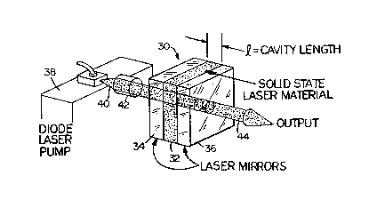
With reference to Fig. 2, a microlaser 30
30 includes a solid state gain medium 32 disposed between a
pair of mirrors 34 and 36. In accordance with the
discussion above in conjunction with Fig. 1, the cavity
length Q between the mirrors 34 and 36 satisfies the
inequality: Q<c/2nvg where vg is the
l~9Z797
bandwidth of the gain medium. Suitable solid state gain
media are Nd:YAG and Nd pentaphosphate. The laser
mirrors 34 and 36 may either be deposited as coatings
directly on opposing surfaces of the laser gain medium
32 or made using thin glass or other appropriate
material and subsequently bonded to the gain medium 32
to form a sandwich structure. For a laser gain medium
such as Nd:YAG, the cavity length would be approximately
several hundred ~m, while for a stoichiometric
compound laser material such as Nd pentaphosphate,
cavity lengths will be typically in the range of 10-100
~m.
In operation, the microlaser 30 is excited by
an appropriate source such as a semiconductor injection
laser or laser array. A diode laser pump 38 is shown in
Fig. 2. A pump beam 40 from the diode laser pump 38 is
focused by an optical focusing system 42 and optically
pumps the microlaser 30 such that it operates in a
single spatial mode. The microlaser 30 then generates
an output beam 44. Alternatively, the diode laser pump
38 may be bonded directly to the mirror 34 of the
microlaser 30 as shown in Fig. 3.
In the case where the absorption length of the
pump laser radiation is longer than the length of the
laser material, an enhancement of the pump laser
absorption can be made by placing the laser material
inside a Fabry-Perot type resonator at the pump laser
wavelength. For example, refering to Fig. 2, the
dielectric coatings on both laser mirrors would have
high reflectivity at the pump laser wavelength in
addition to being properly coated at the wavelength of
the laser material.
The microlaser 30 may be made to operate at
several wavelengths including the 1.32 ~m transition
12gZ7~37
of Nd which would be useful for optical fiber
communications and fiber sensors. Furthermore, the
frequency of the microlaser 30 may be locked to a
secondary frequency reference such as an atomic or
molecular absorption to provide a well defined carrier
frequency as a communications standard. A multiplexed
communications system may be operated by generating side
bands from the frequency locked master oscillator. Such
a system will allow for any communications system to be
10 compatible with any other system because each channel
will have an absolutely identifiable frequency.
The microlaser 30 may be tuned in a number of
ways such as changing the effective length of the
optical cavity. Cavity length may be changed by
15 altering the refractive index of the gain medium or of
some other material contained within the laser cavity.
The mechanism for altering refractive index may be
thermal or electronic by utilizing a temperature
dependent refractive index effect or an electro-optic or
20 piezoelectric effect, respectively. Alternatively, a
piezoelectric or other mechanical device may be employed
to move one of the laser cavity mirrors for laser tuning.
The microlaser 30 can be made quite compact and
stable using microfabrication techniques similar to
25 those used in the semiconductor fabrication industry.
The design of the microlaser 30 renders it able to
withstand significant shocks for operation under adverse
conditions. One application for a microlaser 30 device
would be for fiber optic gyros which require narrow line
30 width operation.
The microlaser 30 may also be operated at low
temperature (from the temperatre of liquid helium at
1.5 Kelvin to just below room temperature). Such
operation will provide for stable, precision frequency
lZ9Z797
output. The spectral gain linewidths for the active
gain materials can become quite narrow at low
temperatures (less than 100 MHz in some cases). By
locking the microlaser 30 to its own gain peak using a
number of well known techniques, an absolute frequency
of operation may be obtained with an accuracy of as
little as a few kilohertz.
It is recognized that modifications and
variations of the present invention will occur to those
skilled in the art and it is intended that all such
modifications and variations be included within the
scope of the appended claims.