Note: Descriptions are shown in the official language in which they were submitted.
~ $~
E5-002
This invention relates to method and apparatus for
acquiring and storing an electronic latent image of a
scene in a fielfl of view and for reducing that stored
image to visible form for purposes of reproduction and/or
display. It relates more particularly to an improved
technique for taking pictures electronically and for
displaying or printing those pictures after they are
taken.
Background of the Invention
Most modern photographic reproduction systems and
cameras are based on either the use of silver halide
film, or the employment of solid state electronic
photosensors for image detection to drive a display, or
the use of an electron beam tube whose sensing surface
receives an image and is scanned with an electron beam
for one-time read-out and separate storage of the
detected picture signals. While all of these prior
systems work reasonably well, each has certain
disadvantages. For example, those cameras using film
require relatively complex shutter mechanisms, and the
film, which is not reusable, must be developed chemically
in order to obtain the picture. Electronic solid state
sensor-type cameras tend to be relatively large and
complicated machines which are relatively expensive to
make. Those electronic cameras which utilize an electron
beam tube, such as a vidicon tube reauire a video tape or
other storage medium to reproduce the pictures acquired
by the tube. That is, they store the picture information
in analog or digital form on a separate magnetic medium.
That medium imposes significant limitations on the amount
of image information that can be stored, thus limiting
the quality of the reproductions made from the sensed
data. A disc or tape buffer memory also makes that type
~k
~ 3~
E5-002
of camera quite bulky, costly and necessitates large
electrical power supplies. It would be desirable,
therefore, to provide a new type of camera which can take
a series of snapshots electronically and reproduce those
pictures without the need to store the picture
information on buffer storage media, such as video tapes
or video disks.
There hav-e been some efforts in the past to produce
materials which can sense and simultaneously store
optical images on multiple loù~cr materials and
subsequently produce hard copy output. One of these
approaches called the Ratsuragawa process and its
derivative, the so-called Canon NP process, were
developed to form electrostatic images for office copying
products. 8Oth of these old processes use a
photoconductive medium comprising a photoconductive layer
and a superimposed dielectric layer. The photoconductive
layer modulates an incoming light image to create an
electrical charge pattern across the dielectric layer.
Toner is then applied to the medium to develop the image.
These processes require precise interactions of corona
ionic charging of the medium, light exposure while
countercharging of the medium and subsequent blanket
exposure of the medium to form a stabilized electronic
image across the medium's dielectric layer. Furthermore,
the Katsuragawa and Canon processes neefl a gas plasma or
open-air environment in order to function; they also
require significant amounts of incoming light, i.e., a
very intense light image, for exposure because the
recording medium used in those processes have relatively
poor sensitivities. Also, these prior techniques obtain
only limited resolutions and they are not capable of
acquiring and storing color images of photographic
quality at photographic speeds.
~ E5-002
Another approach to the development of an electronic
camera system is described in U.S. patent 3,864,035
(Kuehnle). This camera also utilizes an electrographic
recording medium comprising superimposed photoconductive
and dielectric layers. The medium is exposed to a light
image and simultaneously, a corona-producing device
charges the surface of the medium to a peak voltaqe
dependant upon the intensity of the incoming light. Due
to the different light and dark decay characteristics of
the medium, an electronic charge distribution develops
across the surface of the medium's dielectric layer.
That charge pattern corresponds to the incoming light
image and immediately torer is applied to the surface of
the medium to develop that electrostatic image before it
decays. Thus, that patented camera utilizes well known
xerographic and electrofax copying techniaues and the
value of that prior arrangement resides in the packaging
of the various components that carry out those well known
processes into a small camera-size envelope. As noted,
the recording medium described in that patent can store
an acauired image for only a very short time so that the
image must be developed by toner almost simultaneously
with its acc!uisition. This presents certain timing
problems, it also requires that the camera incorporate a
complete toning station which increases the size,
complexity and cost of the camera.
That prior camera system also has a low photospeed,
making it commercially not viable. Large amounts of
light are required to create an image on the medium,
comparable to the exposures needed in xerographic
copiers, e.g., ASA 1.
Another disadvantage of that camera system stems
from its utilization of an electrographic recording
medium incorporating a substrate or base through which
~3~
ES-002
the image being acquired is projected that is made of an
organic plastic material, such as polyester, polyethylene
or the like. ~lthough that substrate is quite optically
clear when the medium is new, due to its low abrasion
resistance, its optical properties begin to deteriorate
rapidly when the medium is used, because scratch marks
accumulate on its surface.
Furthermore, the medium described in that patented
system, even if it could retain an acguired image for a
reasonable period of time, cannot be read-out by the most
effective technique, namely electron beam scanning. This
is because such scanning must take place in a vacuum and
outgassing from the medium's organic components,
particularly the base, produces a sharply reduced vacuum
besides causing ion/electron collisions in the scanning
beam and effecting the beam electrode, making impossible
the retrieval of quality images. Since, out of
necessity, development by toner rather than electron beam
scanning is ~tilized in that prior system, it becomes
essential that the recording medium is discharged by
exposure to a potential near zero in the brightly
illuminated areas; only then is it possible to develop
the image without pronounced fog in the theoretical]y
clear areas of the picture. This means that the lighter
areas of the medium require saturation exposure to
accommodate the innate fogging problem with the toner.
Another electronic imaging technique that does
permit retrieval by electron beam scanning of an
electronically stored image is disclosed in the
publication Electrostatic Imaging and Recording by E.C.
Hutter et al, Journal of the S.M.P.T.E., Vol. 69, January
1960, pp. 32-35. The recording medium or "phototape~ in
that reference, also disclosed in U.S. Patent 3,124,456
(Moore), comprises a transparent polyester base coated on
lZ93(~54
E5-002
one side with a layer of photoconductive material which
is, in turn, coated with a thin layer of a dielectric
material. To record an image on the medium, the
dielectric layer is precharged by a voltage applied
across that layer and then the photoconductive layer is
exposed to a light image while an electric field is
applied across the dielectric layer. The charge on the
dielectric layer decays toward zero with the decay being
most rapid where the optical image is brightest and,
therefore, the photoconductive resistance is the lowest.
After a time corresponding to the greatest difference
between the potentials in the light and dark areas of the
medium, the electric field is turned off and the
discharging process stops, thereby leaving on the
dielectric layer an electrostatic charge distribution
corresponding to the optical image incident in the
medium. The stored image may be developed by applying
toner to the medium or it may be read from the medium by
scanning the dielectric layer with a focused electron
beam to produce an electrical signal corresponding to the
stored image.
Since the ~utter et al system employs a recording
medium incorporating an organic plastic substrate, it has
the same disadvantages as the patented camera discussed
above. Also, in that system, a voltage must be applied
to the recording medium prior to exposure in order to
precharge the dielectric layer of that medium. Since the
precharge bears no relationship to the brightness of the
scene, particularly in its dark areas, the image may be
totally under- or over-exposed, making it difficult to
read. Also, due to imperfections and defects in the
medium's active layers, that precharge may vary across
the surface area of the medium and is, therefore, not
dependable as an exposure reference potential.
~Z93~54
E5-002
That arrangement has several other disadvantages as
well which seriously limit, if not prevent, its practical
application. More particularly, the phototape used in
the Hutter et al system has poor light sensitivity
comparable to the very slowest silver halide films, i.e.,
ASA 1-10. Furthermore, it can store the acquired data on
the medium for only a limited period of time, e.g., a few
weeks, because of charge leakage in the dielectric layer
of the medium. In other words, using a brute force
approach, the Hutter et al system achieves exposure of
the recording medium along a portion of the charge vs.
exposure characteristic curve for that medium yielding
only up to eight levels of the grey scale. Accordingly,
the quality of the images acquired by that system are not
very high. That being the case, it is not surprising
that the pictures retrieved from the medium by electron
beam scanning are of poor quality and inferior to silver
halide film. Furthermore, read-out of the image stored
on the medium is accomplished by detecting a capacitively
modulated current signal from the medium involving
simultaneous movement of many charge carriers in the
medium. Resultantly, the resolution of the detected
picture signal is less than that of the stored electronic
image which, as just stated, was fairly poor to begin
with.
still further, in the process of reading the stored
image for display or reproduction, that image is degraded
by electronic conduction caused in the medium by the
electron beam scanning process itself. In other words,
when the Hutter et al system performs a read operation,
it also tends to erase the image stored on the medium.
This, of course, is completely unacceptable if that
system is to be considered for long or short term storage
lZ~3~54
E5-002
of optical images which may have to be retrieved several
times during the storage period.
Other recording systems are disclosed in U.S.
Patents 3,880,514 and 4,242,433 to Kuehnle et al which do
not reguire precharging of the recording medium. Rather,
those systems charge and expose the medium
simultaneously. In that respect, they are superior to
the Hutter et al recording system; otherwise they are
disadvantaged in the same respects as the latter system.
_umm ry of the Invention
Thus, it is an objective of this invention to
provide an interactive electronic image recording
apparatus in the nature of a microscope or camera system
for the acguisition, storage and retrieval of optical
images in order to compare, view and/or reproduce the
acguired optical data.
Another object of the invention is to provide a
system such as this which has automatic exposure control
and focus capabilities.
A further object of the invention is to provide an
image acquisition and storage system which can record
optical images at a high photospeed and store said images
for a period of several years in parallel form for
subsequent retrieval and further electronic processing in
a serial manner.
Yet another object of the invention is to provide a
system which records an incoming light image on an
optoelectronic storage medium in a manner that produces
substantially no information loss.
Still another object of the invention is to provide
an optical signal acguisition and recording system in
which the recording medium interacts or cooperates with
other components of the system including an
exposure/contrast meter and an electron source for
~293~54
E5-002
optimizing conditions to capture the maximum amount of
information in the incoming liqht image.
A further object of the invention is to provide such
image recording apparatus in the nature of a microscope
or camera that can take high quality pictures
electronically both in black and white and in color.
Another object of the invention is to provide an
apparatus in the nature of a microscope or camera for
retrieving and disp~aying or reproducing latent
photographic images stored electronically on phototape.
A further object of the invention is to provide such
interactive recording apparatus in the form of a
shutterless camera with an autofocus capability.
Another object of the invention is to provide a
lS microscope-camera system which can store a large amount
of information for a long period of time on a taPe-like
optoelectronic recording medium which can be scanned by
an electron beam to read the stored information for
display or reproduction purposes.
Another object of the invention is to provide such a
recording system whose recording medium has segments or
frames for displaying scenes in a field of view
interspersed with frames for storing electronic images of
those scenes.
It is also an object of the invention to provide a
system which records pictures electronically on a
recording medium which, in situ, can be erased and reused
in whole or in part a multiplicity of times.
A further object of the invention is to provide a
system for storing electromagnetic signals on a recording
medium as an electronic pattern and for reading that
information from the medium in a manner that does not
degrade the stored pattern which after a suitab]e number
of scans can be used for image contrast refreshment.
lZ93~54
E5-002
Another object of the invention is to provide
improved apparatus for recording optical images on tape
electronically in black and white or in color for later
read-out by electron beam scanning.
Still another object is to provide such apparatus
which retrieves images stored electronically on an
optoelectronic medium with an improved scanning electron
beam detection system.
A further object of the invention is to provide an
apparatus of the aforesaid type which achieves close
control over the electron beam scan path during the
retrieval or read-out operation.
Yet another object of the invention is to provide a
method of acquiring and storing optical or electrical
images on an optoelectronic recording medium which
produces one or more of the aforesaid advantages.
Still another object of the invention is to provide
a method of retrieving or reading electronic images
stored on an optoelectronic recording medium that
produces one or more of the benefits enumerated above.
Other objects will, in part, be obvious and will, in
part, appear hereinfter.
The invention accordingly comprises the several
steps and the relation of one or more of such steps with
respect to each of the others, and the apparatus
embodying the features of construction, combination of
elements and arrangement of parts which are adapted to
effect such steps, all is exemplified in the following
detailed description, and the scope of the invention will
be indicated in the claims.
Briefly, my new electronic microscope-camera system
uses a special plural-layer, solid state, wholly
inorganic, crystalline, optoelectronic recording medium.
For purposes of this description, the medium will be
lZ93~54
E5-002
described as a flexible tape. It should be understood,
however, that the medium may also be implemented as a
disk, plate or drum. The medium, e.g. tape, includes a
transparent inorganic base, a photoconductive modulator
on the base and a dual-material dielectric storage layer
on the modulator. The tape is controllably and
simultaneously electrically charged and exposed at
photospeeds about 1000 times faster than all previous
systems, with the charging means acting as a photographic
shutter so that it acquires and stores precise electronic
images in its storage layer for immediate or delayed
read-out. In one apparatus embodiment, the acquired
electronic images can be subseauent to the imaging step
by exposure in the dark to a high energy electron cloud
for the purpose of removing the initial bias electron
charges from the tape. To read or retrieve the pictures
stored on the tape, the tape is scanned by a finely
focused electron beam and the latent images thereon are
read-out in analog form and digitized. These binary
picture signals, now in serial form, may be processed by
conventional electronic circuitry for display or to
reproduce hard copy, or they may be stored on other
storage media for later use.
Thus, the present system performs unlike those prior
electronic imaging systems discussed at the outset which
digitize the incoming picture information immediately
and, therefore, reguire a buffer memory for intermediate
storage of an equivalent image on a magnetic medium such
as video tape. That is, whereas those prior systems use
the photosensitive medium many times as an acauisition
element, the information must be stored elsewhere. In
the system described herein, the photosensitive medium
itself stores the pictures until the user wishes to
retrieve those pictures in analog form for display or
1~93~54
11 E5-002
reproduction. As we shall see, the recording medium and
the remaining elements of my system interact and
cooperate optically and electronically to optimize the
exposure of the recording medium under the prevailing
light conditions in the instrument's field of view so
that the image recorded on the tape is of the highest
resolution and has many steps of grey (dynamic range) and
large contrasts.
As will be seen later also, the electronic images
stored on my medium are read nondestructively from the
medium so that the same images can be read numerous times
and, in fact, the images stored on the tape can be
refreshed from time to time if multiple read-out should
slightly affect the stored signal level. Thus, my system
can retain high guality electronic images for a prolonged
period, making it especially useful for longterm or
archival storage of optical images. On the other hand,
if desired, the tape can be erased fully and reused
repeatedly so that the system is applicable to short-term
storage of optical signals as well.
In my recording system, a projector, which may be an
optical enlarger or reducer, projects a light image onto
the recording medium which is supported by a transparent
platen at the focal plane of the projector. The
projector optics account for the presence of the medium
which has a high refractive index and the projector
includes a motorized focus adjustment. The platen
supporting the tape also incorporates an array of filter
stripes and another array of photosensitive stripes which
are flush with the tape and which respond to different
light intensities over the image area by producing
corresponding electrical signals. These intensity
signals are used to generate a set of control signals
which are applied in a feedback arrangement to adjust the
"` lZ93~S4
E5-002
12
projector's focus so that the image projected onto the
recording medium is brought into sharp focus
automatically before each picture is taken.
Every optoelectronic recording medium has a charge
vs. exposure characteristic curve which is a measure of
the medium's sensitivity or responsiveness to light at
different exposure levels, comparible to the ASA rating
of conventional silver halide photographic film.
Conventional cameras and recorders utilize a separate
light sensor to set the exposurè to suit the film being
used. In the present system, those same photosensitive
stripes on the platen that are flush with the tape are
used to measure the incoming light energy and contrast to
set the charging current and duration for exposure so
that the total incoming energy flux is placed at the
optimal sensitivity region of the particular recording
medium or tape being used. Therefore, there is little
likelihood of the medium being overexposed or
underexposed during the taking of the picture.
After the camera has been focused and its exposure
set automatically as aforesaid, the picture is taken,
i.e., the tape is exposed to an optical image or signal.
~uring this exposure step, while the incoming optical
image is projected onto the tape, an electron source
deposits a cloud of electrons on the surface of the
tape's dielectric storage layer, and at the same time the
active layers of that medium are subjected to a very
intense electric field caused by the electron deposition
on the storage layer and a counter-potential at an
electrode layer adjacent to the base. The energy in the
~light image focused onto the medium is absorbed in the
tape's photoconductive modulator, thereby creating
electron-hole pairs in that photoconductor. Under the
influence of that field, the positive carriers or holes
lZ93~i54
13 E5-002
tunnel through an interface or barrier zone ~field
effect) comprisiny one component of the dual-material
storage layer to the underside of the other component,
namely a dielectric storage zone, while the negative
charges or electrons are conducted away from the
photosensitive medium via the electrode layer to the
battery. The positive charges become trapped or "pinned"
to the underside of the dielectric zone and as soon as
the electric field is turned off, the interface layer
acts as a barrier to prevent any thermally generated or
image unrelated photogenerated charges from tunnelling
B throughlinterface layer and thus accidentally
neutralizing the positive image-related charges which are
pinned, as charge centroids, at the underside of the
dielectric zone.
The number of electron-hole pairs produced at any
location in the image area depends upon the amount of
light impinging upon the photoconductive layer at that
location, thus, translating the incident photonic energy
into an electronic equivalent in the medium which is
stored as a distribution of positive charges at the
underside of the medium's dielectric layer.
Substantially all of these positive charges are matched
by an equal number of negative charges, or electrons,
which reside opposite the positive charges in the surface
of the die~ectric layer, having been deposited there by
the electron source. Thus, the tape's photoconductive
modulator modulates the movement of charge carriers in
the medium in accordance with the incoming light image to
create a distribution of electronic domains across the
upper and lower surfaces of the dielectric layer to form
the electrical analog of the image which is projected
onto the tape. As will be described in more detail
later, the recording medium has a high degree of
lZ93(~54
E5-002
14
perfection and is very thin with the result that the
charge distribution on the medium's image area forms a
very accurate noise-free representation of the optical
image in the camera's field of view.
At the completion of the exposure step, the
electronic images on the tape may have their charge
biases removed by subjecting the surface of the storage
layer to a stream of energetic electrons from an electron
source. This clears the surface of the dielectric layer
of all negative charges that are not bound there by
corresponding positive charges reposing at the underside
of the dielectric layer. The removal of those free
charges eliminates directional dark currents which could
form background noise. Even in those applications where
the removal of excess e]ectrons at the surface of the
storage layer is not sought as noted above, with the
removal of all but image-related electric fields, any
thermally generated carriers in the photoconductor (dark
current) cannot tunnel through the interface layer and,
therefore, leave unaffected the electronic image which is
stored in the dielectric zone or layer. Resultantly, an
electronic image of unusually high auality is stored on
the medium and will remain there for a year or more
unless that image is erased intentionally or another
image is recorded at that same location on the medium.
It should be noted also that the "pinned charges" do not
drift laterally in the dielectric zone so that the full
resolution of the original image is retained in that
zone.
The optoelectronic image-storing medium or tape
described herein is conveniently spooled as a strip or
ribbon in the recording apparatus, which may be a
microscope or camera, and advanced frame by frame into
the focal plane of the apparatus so that images can be
12~3(~54
E5-002
recorded on successive frames of that tape. To
facilitate retrieving the information on the tape,
fiducial marks and timing tracks may be recorded on the
tape along with the optical images to define those
storage locations or frames. When information is being
read from from the tape, these markings are detected and
used to develop electrical signals for controlling the
recorder's tape advance mechanism to reposition the
frames containing the desired optical information
accurately for read-out of that stored data. Such
markings are also used to initialize and align the
electron beam scan as will be described in detail later.
With the aid of recorded marks on the tape, the tape
can be repositioned to bring a selected frame thereof
into position in front of an electron gun. The gun
thereupon emits a finely focused electron beam which
sweeps across the surface of the tape's storage layer in
a raster-type scan under the control of a scanning
circuit. The impinging electrons penetrate that surface
slightly and produce secondary electron emission from
that layer proportional to the number of charges
deposited during exposure on each element of the picture
and held by the internal electric field. ~ collector
detects the number of emitted secondary electrons at each
point in the scan and produces a corresponding electrical
signal which is representative of the stored image. The
electron beam initially searches for the specific
fiducial mark on each frame to attain a zero position for
the drive scanning ciruit so that the track of the beam
on the medium will follow the filter lines which were
exposed onto the frame and be guided precisely during the
scanning process. The picture signal produced thusly by
scanning the tape can be fed to a display, or a printer,
1293(~54
E5-002
16
or it can be s~ored on a magnetic tape or disc for later
use.
The present system can take pictures in black and
white or in color. In the latter event, the tape is
S exposed through a filter array on the tape platen
consisting of very fine interlaced red, green and blue
color lines which coincide with the scan lines of the
electron beam raster. Thus, when a picture is taken, the
information stored electronically on the medium consists
of three interlaced images corresponding to the red,
green and blue color components of the optical image
projected onto the tape. To retrieve or read that stored
color image d~ring a read-out operation, the electron
beam is caused to execute three successive scans across
lS all of the image lines of each color. Thus, the electron
collector generates a set of three analog signals
representing the red, green and blue color information
stored electronically on the recording medium. These
signals, which are in serial form, are then amplified,
digitized, color corrected and otherwise processed in
ways well known in the color graphics art to produce
picture signals for controlling a color display or color
printer. The sensitivity of the electron collector-
amplifier, combined with the nearly noise-free perfection
~5 of the optoelectronic recording medium, gives my system
extremely high sensitivity and fast response, e~uivalent
to a silver halide film speed in the order of ASA 3,000.
The optoelectronic recording medium or tape that is
used in this recording system can be scanned numerous
times without destruction or even material degradation of
the recorded information. In fact, the image stored on
the medium can be refreshed from time to time with the
aid of the electron source if need be to restore its
original distributed charge potentials and, thus, its
12913(~S~
E5-002
17
contrast. If, however, it is desired to record other
optical images on the medium, the stored electronic
images can be erased quite easily by exposing the medium
briefly to ultraviolet light. This short wavelength
energy renders the dielectric layer of the medium
sufficiently conductive to neutralize the electronic
charges stored at opposite surfaces of that layer.
When my system is implemented as a microscope or as
a camera of the single lens reflex type, the medium
disclosed herein is preferably made as a flexible strip
or ribbon with recording frames alternating with
transparent or translucent viewing frames. In the case
of the microscope, the operator can look through a
viewing frame at an object being examined before taking a
picture of that object on the next recording frame. In
the case of the camera, the field of view may be
projected as a virtual image onto a viewing frame area so
that it can be observed through the camerals view finder
prior to taking the picture to be s~ored on the next
recording frame. My apparatus also includes a tape
transport mechanism, the required logic circuitry and
battery power supply to enable the apparatus to advance
the tape accurately and take pictures automatically at
the touch of a button on the camera housing. As will be
seen, the amount of electrical energy needed to deposit
the electronic images on the recording medium and to
retrieve those images is quite low so that the unit can
be lightweight, compact and portable. Also, the
electron-producing sections of the recorder and the
recording medium are contained in an evacuated
compartment in the recorder housing so that lenses and
batteries can be changed in the usual way without
affecting the operation of the apparatus of the medium.
Therefore, my recording system should find wide
lZ93C~
E5-002
18
application whereven the acquisition, long or short term
storage and subsequent retrieval of visual information is
desired.
Brief Description of the Drawings
For a fuller understanding of the nature and objects
of the invention, reference should be had to the
following detailed description, taken in connection with
the accompanying drawings, in which:
FIG. 1 is an isometric view of an interactive
electronic image recording system embodying the invention
implemented as a microscope;
FIG. 2 is a sectional view on a larger scale taken
along line 2-2 of FIG. l;
FIG. 3 is a fragmentary isometric view on a still
larger scale showing the recording medium or tape used in
the FIG. 1 system;
FIG. 3~ is a similar view showing a portion of the
FIG. 1 system in greater detail;
FIG. 4 is a sectional view on an even larger scale
taken along line 4-4 of FIG. 3;
FIG. 5 is a view similar to FIG. 3 showing a portion
of the FIGS. 1 and 2 system in greater detail;
FIG. ~ is a sectional view taken along line 6-6 of
FIG. 5.
FIG. 7 is a diagrammatic view illustrating the
exposure of the FIG. 3 medium.
FIG. 8 is a graph showing the mode of controlling
exposure.
FIG. 9 is a view similar to FIG. 7 which helps to
explain the passivation of the FIG. 3 medium
FIG. 10 is a graphical diagram that helps to explain
that passivation;
FIG. 11 is a view similar to FIGS. 7 and 9 showing
the electronic image stored on the FIG. 3 medium; and
1~93~54
E5-002
19
FIG. 12 is a diagrammatic view of a complete optical
image acquisition, storage and printing system embodying
my invention.
Detailed Description of the Preferred Embodiment
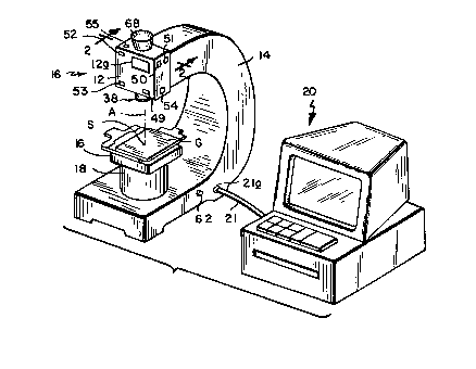
Referring now to the drawings, FIGS. 1 and 2 show my
interactive electronic image recording system. For
purposes of this description, the system takes the form
of a microscope-camera 10 capable of acquiring and
storing electronic images of very small specimens or
objects. However, the invention could just as well be
implemented as a different type of recorder, such as a
camera, by substituting the appropriate camera optics or
lens system.
The microscope 10 comprises a rigid housing 12 which
is supported by a stand 14 above a standard X-Y-Z slide
table or positioner l6 mounted to a pedestal 18
projecting up from the base of the stand. The positioner
16 is arranged to support and position a glass slide G on
which the specimen S to be viewed is placeA. Using the
positioner 16, the specimen S can be spotted on the
viewing axis ~ of the microscope 10. After microscope-
camera 12 takes a picture of specimen ~S, which is stored
on an optoelectronic recording medium 34 (FIG. 2) inside
the microscope, that apparatus can be operated in a read-
out mode to retrieve the stored image for display orreproduction using a CRT/printer unit indicated generally
at 20 connected electrically to the microscope by a cable
21.
As best seen in FIG. 2, the microscope housing 12 is
divided into a plurality of internal compartments. More
particularly, there is a tape transport compartment 22 at
the bottom of the housing which contains a pair of rotary
spindles 24 and 26 for supporting take-up and let-off
- ` lZ93~54
E5-002
spools or reels 28 and 32~respectively~between which
stretches the optoelectronic recording medium which is in
the form of a long phototape 34. When the spindles 24
and 26 are rotated, the tape is advanced along a focal
plane indicated generally at P which constitues the
exposure position of the tape.
The bottom wall of housing 12 is formed with a
generally cylindrical cavity 35 which intercepts
compartment 22 directly opposite plane P. The inner end
of that cavity is closed by a transparent glass platen 36
that isolates compartment 22 from cavity 35. While in
FIG. 2 the platen 36 is shown separated from the tape, in
actuality, its surface 36a positions the tape at focal
plane P. The platen may also constitute an optical
element in the microscope's optical path to produce field
flattening, color correction, filtering, etc. of the
incoming optical image. Furthermore, as we shall see,
the platen has special light sensing capabilities that
are used to foc~s the microscope automatically prior to
taking a picture and to set the exposure duration when
the picture is being taken.
The camera's movable lens unit, indicated generally
at 38, is rotatively mounted in cavity 35 and the
microscope is focused onto specimens by controlling a
servomotor 39 that moves the lens unit axially very
precisely in one direction or the other. Of course, the
instrument can also be focused man~ally by appropriately
moving unit 38.
The tape 34 is moved back and forth between the two
spools 28 and 32 by reversible servomotors 42 which
rotate spindles 24 and 26 respectively. By applying
currents to these motors 42 of the appropriate
polarities, the tape 34 may be kept taut and moved in
either direction to position a selected tape frame on
~93C~S~
21 E5-002
platen 36 at the microscope's focal plane P. In some
applications, the tape may be advanced by other means
such as a capstan or a linear or eddy current motor using
a metallized margin of the tape itself.
The mechanism for transporting tape 34 may include
other components, such as tape edge guides and a tape
gate for actually locating each increment or frame of the
tape at an exposure position in the image plane P.
However, for ease of illustration these components, which
are found in many conventional automatic cameras, have
not been shown in the drawing figures.
Microscope 10 includes another compartment 46 which
contains the camera's control section 48. That section
includes a microprocessor and current drivers for
providing the drive signals for the drive motors 42 and
for the camera's gate (if present). The makeup of
section 48 and the programming of its processor will be
obvious from the control functions to be described. When
the operator pushes a recessed FORWARD button 50 (FIG. ])
in the side wall of housing 12, the control section 48
will apply a selected number of pulses to motors ~2 to
shift the next tape increment or frame into the exposure
position at the image plane PO Signals from control
section 48 to the motors will shift the tape frame by
frame in the opposite direction when a recessed REVERSE
button 51 on the side of the housing 12 is depressed.
Preferably, buttons 50 and 51 and the camera's other
control buttons to be described are capacitive "touch"
buttons built right into the wall of housing 120 These
other control buttons include a FOCUS button 49 which may
be depressed to automatically focus instrument 10, an
EXPOSE button 52 which initiates the recording of an
optical signal on the tape 34, a R~AD button 53 which
initiates a read operation on the tape to produce picture
lZ93~:35~
E5-002
22
signals corresponding to an image stored on the tape and
an ERASE button 54 which is depressed to erase an image
already stored on the tape in microscope-camera 10.
Also, a tape frame counter 55 is mounted in the top wall
of housing 12.
The power for motors 42 and for control section 48
and the other electromechanical parts of the apparatus
derives from a power supply 56, including batteries,
contained in a compartment 58 of housing 12 located above
compartment 46. Appropriate electrical conductors are
provided between these parts as wires or printed circuits
inside the housing. Access to the interior of the
battery compartment 58 is had by removing a small cover
12a tFTG. 1) in the front wall of housing 12. Preferably
also, the batteries in the power supply 56 are of the
type that can be recharged by connecting them to a source
of DC power by means of a female connector 62 located at
the bottom of stand 14 as shown in FIG. 1.
~ousing 12 also has a large compartment 64 which is
aligned with the axis of lens unit 38, which axis
coincides with the optical axis A of the microscope.
Compartment 64 contains the various stationary lenses 66
that comprise the microscope. These are all centered on
axis A and the operator uses the microscope to observe
specimen S by looking through an eyepiece 68 in the top
wall of housing 12.
Still referring to FIG. 2, microscope-camera 10 a]so
includes a field emission device or electron source 74
which is slidably mounted in the housing just above
platen 36. The source can be moved between an extended
position shown in solid lines in that figure wherein it
overlies the tape frame at the focal plane P and a
retracted position shown in dotted lines in that same
figure in which the gun is located in housing compartment
lZ930~4
23 64421-394
46 away from the tape. While source 74 may be shifted between its
two positions by any suitable means, in the illustrated apparatus,
it is moved by a servomotor 78 located in compartment 46 and
coupled to source 74 by way of a rack and pinion arrangement. The
electron source 74 is normally located in its retracted position
so that it does not obstruct the operator's view through the
microscope. However, during the exposure process, the source is
moved to its extended position overlying the tape by motor 78
under the control of section 48. Section 48 then causes source 74
to direct a cloud of electrons from discharge points 74a of source
74 against the upper side of the tape frame present at the focal
plane P. As we shall see, the upper surface of the tape frame at
plane P becomes charged with these negative carriers, enabling
that frame to acquire and store an electronic image corresponding
to the optical image projected onto that frame by the instrument's
lens unit 38. The amount of the charge is controlled in terms of
time and magnitude to assure the capture of the maximum amount of
information contained in the image to be recorded. As we shall
see, the electron source 74 is also used to eliminate the electri-
cal bias field from each tape frame after the exposure of thatframe by removing excess charge carriers from the frame.
Microscope-camera 10 also includes an electron gun 84
located in a large housing compartment 86 to the left of compart-
ment 64 and used when instrument 10 is operated in its read-out
mode. Unlike source 74, electron gun 84 directs a finely focused
beam of electrons to the exposed tape frame present at a read
plane or position R in compartment 86 that is defined by the
bottom wall of that compartment. Gun 84 is controlled so that the
electron beam sweeps out a raster on the upper surface of that
^`` lZ93~5~
E5-002
24
frame by a circuit 88 located in a housing compartment 92
positioned just to the left of compartment 86. Since
tape 34 is temperature dependent, preferably the gun is a
cold cathode device that does not generate heat.
During read-out, the scanning electron beam from gun
84 causes secondary electrons to be emitted from the tape
frame being scanned whose numerical distribution by area
elements (pixels) represents the electronic image stored
on that frame. These secondary electrons are collected
by an annular electron collector 94 located near the top
o~ compartment 86 which thereupon produces a signal which
is the electrical analog of the stored image. That
signal is applied to a read-out circuit 96 contained in a
housing compartment 98 to the right of compartment 86
where it is amplified, digitized and otherwise
conditioned before being applied to the various
conductors of the connector 21a to which cable 21 is
coupled as shown in FIG. 1. Those picture signals are
then fed by way of that cable to terminal 20 where the
retrieved image can be viewed or reproduced.
In the microscope-camera 10 speci~ically illustrated
herein, the same tape 34 is intended to remain
permanently in the housing compartment 22. ~ccordingly,
that compartment, along with compartments 46, 86 and the
portion of compartment 64 below the lowest lens 66, is
maintained under a high vacuum, in the order of 10-8
Torr. To hold the vacuum, airtight seals tnot shown) are
provided between platen 36 and the wall of cavity 35 and
between the lowest lens 66 and the wall of compartment
64. These compartments are thus free of dust, moisture
and other contaminants that could interfere with the
electrons from the electron sources 74 and 84.
Refer now to FIGS. 3 and 4 which show the
optoelectronic tape 34 in greater detail. It is composed
1293~54
E5-002
of a large number of imaging segments or frames 34a and
an equal number of viewing segments or frames 34b which
alternate along the length of the tape. The tape is made
in toto of inorganic materials, as opposed to organic
plastic materials. Therefore, it does not produce
dreaded contamination caused by outgassing in the high
vacuum environment of the microscope and it will,
B therefore, not ~ any adverse effects on the electrons
emmitted from guns 74 and 84.
Basically, the tape is a unitary hetero-epitaxially
grown structure comprising a flexible, optically clear
tfrom 0.2 to 5.0 micrometers) ribbon-like monocrystalline
sapphire (A12o3) base or substrate 102. Added to base
102 in each imaging area 34a of the strip are a thin
(i.e., about 10,000 A) modulator 104 composed of a
photoconductive material, such as silicon (Si) or gallium
arsenide (GaAs~, and a very thin (i.e., 1,000 A) dual-
material storage layer 106. A very thin phosphorus-doped
zone 104a of modulator 104 (i.e., n-doped with fixed
positive charges) is present ad~acent base ln2 to serve
as an electrode. The remaining zone 104b of modulator
104 is free of additives.
The dual-material storage layer 106 is composed of a
very thin (i.e., about 1,000 A) storage zone or layer
106a made of a suitable dielectric material such as
silicon nitride (si3N4) and an ultra- thin (i.e., about
30 A) interfacial zone 106b of an anisotropic dielectric
material such as silicon dioxide (SiO2) at the underside
of zone 106a. Zone 106b exhibits electrical insulating
behavior that prevents penetration of thermally generated
or even photogenerated charge carriers in modulator 104
to the undersurface of storage zone 106a; but zone 106b
does allow tunnelling through to the storage zone 106a of
photogenerated charge carriers under the influence of a
1293(~5~
26 64421-394
suitable superi~posed strong orthogonal electrical field
through the tape layers 104a, 104b, 106b and 106a. In other
words, charge carriers from the modulator 104 that have
tunnelled through zone 106b under the influence of an applied
field are "pinned" to the underside 106c of storage zone 106a in
so-called charge centroids. In the absence of that field, zone
106b prevents additional carriers from reaching the storage zone
and disturbing the properly accumulated charge count there.
Thus, zone 106b traps all photogenerated positive carriers
created during the exposure step in storage zone 106a, thereby
storing an electronic signal pattern spatially in that zone of
the tape and preventing also any lateral movements of said charge
carriers in zone 106a so that an image having exceptional
resolution is maintained for many years.
The tape 34 is very thin, being only a few microns thick,
so that it is flexible enough to be wound easily onto reels 28
and 32. It may be made, for example, by the process described
in applicant's copending Canadian patent application Serial No.
539,271, filed on June 10, 1987 and entitled Method and Apparatus
For Making Inorganic Webs and Structures Formed Thereof. The
imaging areas 34a of the tape have extraordinary properties,
among which are extremely high sensitivity or photospeed,
comparible to a silver halide film speed in the order of ASA
3,000. Each of these areas is imageable at low energy levels
(e.g. 20 electrons minimum/pixel) due to low inherent noise
(defects) and dark currents (threshold minimums). Thus, each
of the areas has the capacity to acquire a very high quality
,;
(~ ,...
:, ... ;.
1293(~S4
26a 64421-394
electronic image corresponding to the optical image projected
onto it by the microscope's lens unit 38. Furthermore, because of
the barrier and trapping
., .
~Z93~54
E5-002
27
functions of the tape's unique dual-material storage
layer 106, an image can be stored on the tape areas 34a
for several years without any appreciable degradation of
that image.
The images stored on the tape frames 34a can be read
by scanning the surfaces ~06d of those areas using the
electron beam from gun 84 to produce exceptionally high
guality displays or reproductions of the stored images.
If desired, the image on each tape frame 34a can be
erased by exposing the frame to ultraviolet light from a
U.V. lamp 110 (FIG. 2) mounted in housing compartment 64
just above tape 34. This radiation discharges the
frame's dielectric layer 106 enabling the film frame to
be reused repeatedly and the frame area does not lose its
optical signal acc!uisition and storage capabilities with
such repeated usage.
The base or substrate 102 of tape 34 is ~uite
transparent so that the segments of that substrate in the
viewing frames 34b of the tape constitute windows. When
one of these frames is located at the microscope's focal
plane P, the operator sighting through eyepiece 68 can
see right through that frame to the object being viewed,
i.e., specimen S (FJG. 1).
In another application, as when the tape 34 is
processed in a single lens reflex camera incorporating my
invention, the surface of the substrate 102 may be
abraded, etched or otherwise treated in the tape frames
34b so that it has the characteristics of frosted glass.
If the modulator 104 and storage layer 106 are etched
away to form the viewing frames, then only the clear
sapphire substrate remains in the optical path for
viewing the scenery as through a telescope; however, the
refractive index of the substrate must be considered when
the additional lens elements are calculated for the
1293¢5~
E5-002
28
viewfinder subsystem. In any event, a virtual image of
the scene in the camera`s field of view will be projected
onto the viewing frame located at the camerals focal
plane and that image can be seen from behind the frame by
looking through the camera's viewfinder eyepiece. It
should be noted that the red, green, and blue filter
lines, which represent the primary colors, will appear as
white to the viewer (daylight spectrum). Also, of
course, the phototape may consist entirely of imaging
frames for use with an instrument having a seperate
viewfinder.
Referring to FIG. 3, proper exposure of the imaging
frames 34a of the tape requires that voltages from power
supply 56 be applied to the conductive zone 104a at those
frames. Accordingly, in the forward edge margin of each
imaging area, the material zones 106a, 106_, and 104a to
104_ are etched away so that a conductive strip 112 can
B be ~e~ down on conductive zone 104a. Tf desired, in
some applications the strip 112 adjacent each frame 34_
may be isolated electrically from the similar strips
associated with the other frames of tape 34 so that
electrical connections may be made to each frame
independently. As shown in FIGS. 2 and 3, when a
particular imaging frame 34a is present at the
microscope's focal plane P, a contact finger 118 at the
front of compartment 64 contacts strip 112. ~s shown in
FIGS. 2 and 4, that contact finger is connected in
parallel to switches 122 and 124 in the microscope's
control section 48. Alternatively, electrical
connections to the strip may be made through the spool
spindle 24 or 26.
As best seen in FIG. 2, an optical detector 134
connected to control section 4~ is located at the
righthand corner of compartment 64 above the tape. It is
lZ~3~15~,
29 E5-002
arranged to detect the transition from a transparent
viewing frame 34b to the next opaque imaging frame 34a,
i.e., the leading edge of an imaging frame. Whenever
section 48 receives a detector 134 signal, it indicates
that a viewing frame is positioned properly at focal
plane P. That signal also indicates that the previous
imaging frame 34a (or the tape leader) is located at the
readout plane R in compartment 86 for a read operation on
that frame by electron gun 84. P second similar optica]
detector 136 is positioned just above the tape on the
righthand wall of compartment 86. Detector 136 emits a
signal to section 48 whenever it detects the leading edge
of a frame 34a, thus indicating that a frame 34a is
positioned properly at focal plane P, ready for imaging.
15 Thus, the detectors 134 and 136 together provide position
signals to section 48 enabling that section to control
servomotors 42 to position a tape frame 34a or 34b at
either the exposure position at focal plane P or the
scanning or readout position at readout plane R.
Refer now to FIGS. 5 and 6 of the drawings which
depict the portions of microscope-camera 10 that set
automatically the instrument~s focus and its exposure in
accordance with the prevailing lighting conditions.
These parts include an array of numerous thin, parallel,
transparent, abutting, bandwidth-limited, electrically
insulating, color filter stripes 142 formed on the platen
surface 36a that supports the tape 34 at the camera's
focal plane P. The stripes extend longitudinally and
parallel with respect to the tape edge so that they
coincide with the scan line pattern associated with the
electron beam from gun 84. Although the drawing figures
illustrate stripes 142 as being relatively thick and few
in number, in actuality there may be several thousand
stripes in the array on platen 36, each stripe being in
lZ~3~54
E5-002
the order of only a few microns wide and a few microns
thick.
The filter stripes 142 on platen 36 consist of very
fine abutting parallel red (R), green (G), and blue (~)
films which divide the incoming light image into its
color components. Thus, when a tape frame 34a is exposed
at plane P, the image applied to the frame consists of
red, green and blue color components of the object being
viewed which are interlaced on the frame as shown. In
other words, the picture information for each color
component of the picture is stored every third line on
the tape frame. The color filter lines coincide with the
raster path of the scanning electron beam from gun 84,
when that imaging frame is located at read-out plane R in
compartment 86. The width of the scanning electron beam
may be slightly less than the width of the filter stripes
to compensate for any residual skew and any minute
misregistration of the tape frame 34a between its
exposure position at plane P and its read-out at plane R.
Interspersed with the stripes 142 are a series of
thin, photoconductive stripes 143 featuring large band
width sensitivity. The function of stripes 143 is to
detect incident light levels when their photo-currents
are all integrated and image contrast (focus) when their
differential photo-currents attain the widest amplitude
spread. Suitable photoconductive materials for stripes
143 include silicon or gallium arsenide (GaAs).
Electrical leads 144a and 144b lead from the conductive
layers of each stripe 143 to the camera's control section
48. The number of photoconductive stripes 143 may be
only 10 or 100 out of the several thousand filter stripes
142, placed at ninety line intervals, for example. When
a voltage is applied across each stripe 143, the current
through that stripe will provide a measure of the
`` 1293054
31 64421-394
intensity of the light incident on that stripe. The photodetector
stripes 143 are quite opaque as compared to the color filter
stripes whose transparency exceeds 90% in the bandwidth limited
region but since they are relatively few in number they attenuate
the incident light only minimally.
Preferably, a transparent conductive film or layer 145
overlies stripes 142 and 143, clearing the latter as shown in FIG.
6, to form an electrode which is connected by a lead 145a to
control section 48. During the exposure process, control section
48 biases layer 145 negative with respect to the tape conductive
layer so that that frame is electrostatically attracted to platen
36 and held closely to the filter stripes 142. On the other hand,
when the tape is being moved before and after exposure, section 48
applies a DC voltage of the opposite polarity to layer 145 so that
the tape is electrostatically repelled from the platen 36 to
minimize scratching of the tape base 102.
When the operator depresses the EXPOSE button 52 (FIG.
1) to record an optical signal on a tape frame 34a just prior to
exposure of that frame, control section 48 connects stripes 142 to
the power supply 56 so that a constant voltage is applied in
parallel across all of the photosensitive stripes 143. The con-
trol section then samples and integrates the currents through the
stripes to develop a total flux (TF) signal which represents the
total light flux incident on the tape frame 34a being exposed.
That TF signal is then used by control section 48 to control the
charging current flowing during the separately computed on-time of
the electron source 74 during the exposure process; the control
section also "finds" the stripe producing the smallest signal,
representing the darkest part of the image, the magnitude of that
signal, referred to herein as the exposure
. ,~
1~3(:~54
E5-002
32
duration (ED) signal, being used by section 48 to control
the "on time" of the electron source 74 during the
exposure process, the mathematical product of current and
"on time" being proportional to the incident light flux.
Refer now to FIG. 7 which shows the electrical
environment of the film frame 34a during exposure and
FIG. 8 which depicts a typical characteristic curve C for
the frame being exposed. Effectively, control section A8
controls a variable resistor ~ connected in series with
electron source 74, a 5-100 volt tap of power supply 56,
switch 122 and tape imaging frame 34a at layer 104a
thereof so that the darkest part of the light image being
projected onto the frame receives a selected minimum
exposure, i.e., at least 109 photons/cm2 corresponding
10-3 ergs/cm2. In a typical case, the charging current
in the FIG. 7 circuit is under one ampere and persists
for one microsecond to one second (or more), depending
upon the amo~nt of light incident on the tape. ~ach
incident photon produces one electron-hole pair in
modu~ator layer 104 as shown in FIG. 7. In the portions
of modulator 104 where the light image is darkest, the
incident photons emanating from a faint image typically
produce in the order of 3.108 electrons/cm2. For the
brightest parts of the modulator, there may be in the
order of 3-1011 photogenerated electrons/cm2. Thus, the
charges stored at different locations on layer 106 may
vary from, say, 2n electrons/pixel to 20-103
electrons/pixel. The difference yields a dynamic range
of 1000:1, permitting the retrieval of far more than the
desired thirty two different grey levels G in the image
being recorded on the tape frame 34a, as shown in FIG. 8.
The electric field across the tape causes the
photogenerated electrons to move toward conductive layers
104a from where they are conducted away to the ground
1293(:~54
~5-002
33
plate of the battery 56 via conductive layer 104a. The
photogenerated positive carriers or holes move toward
tape storage layer 106. Under the influence of the
strong superimposed external field extending between the
electrode layer 104a and the virtual electrode formed by
electron deposition on surface 106d and the additional
internal field formed between negative electronic charges
on the surface 106d of layer 106 and the innate positive
potential of the holes, these holes tunnel through the
interfacial zone 106b and are trapped in the under-
surface 106c of the dielectric zone 106a in numbers that
are in direct proportion to the image brightness in the
different parts of the image area I of the frame 34a.
B -~ positive charges are balanced by equal numbers of
electrons from source 74 that repose on the surface 106d
of layer 106 as shown in FIG. 7. A~though the charge
domains or numbers of electrons stored at ad~acent pixels
on tape surface 106d may vary to establish the contrast
or grey le~vels in the stored electronic images, the
potential versus electrical ground is egualized
throughout the ~rame area. Thus, during exposure,
control section 48 charges frame 34a to a voltage and for
a time so as to operate on the o~tim~m segment of the
tape's characteristic curve C/und7er the prevailing
lighting conditions. Accordingly, there is no
possibility of over-exposure or under-exposure of the
picture being taken by camera 10 and stored on each tape
frame 34a in an exposure energy range from a minimun of
10-3 ergs/cm2 to 10 ergs/cm2.
As noted above, the photosensitive stripes are also
used to focus the camera when a viewing frame 34b is
located in the focal plane P. Accordingly, the specimen
S (FIG. 2) will assuredly be in focus when seen through
eyepiece 68 and frame 34b or when photographed on the
lZ93~5~
~S-002
34
next imaging frame of the tape. More particularly, when
control section 48 receives a signal from detector 134
indicating that a viewing frame 34b is positioned at
focal plane P, it provides a constant voltage across
stripes 143 and samples the current signals from these
stripes as described above. When an out-of-focus image
is projected onto the array of stripes which, in fact,
defines the camera's focal plane P, that image will be
blurred and will have little or no gray level
differentiation or contrast over the image area in plane
P. Accordingly, the output signals from the array of
stripes 143 will have a corresponding lack of
differentiation. As the projected image at plane P is
brought into focus, there is greater contrast between
light and dark areas of the projected image. Ultimately,
when the image projected onto the stripe array is in
exact focus, the differences between the lighter and
darker areas of the image will reach a maximum, as will
the amplitude spread of the differential photo currents
from the stripes 143 corresponding to those image areas.
During the focusing process, control section 48
repeatedly samples the set of signals produced by the
stripe array. During each such samp~ing, after pein~ J
digitized, the signals from the stripes are ~u~sh~s~h~
to develop a set of difference signals which are averaged
and inverted to produce a feedback signal to control the
motor 39 that moves lens unit 38. If, as a result of a
given sampling, the motor 39 is driven to improve the
focus, the feedback or difference signal resulting from
the subsequent sampling of the stripe signals will
reflect that fact and the driving of the motor 39 will
continue until the feedback signal is reduced to zero.
On the other hand, if there is no improvement in the
focus after a few samplings and consequent lessening of
`` ` lZ~3t35~5~
Es-on2
the feedback signal, indicating that the lens unit 38 is
being moved in the wrong direction to achieve focus,
control section 48 will reverse the polarity of the
voltage applied to motor 39 so that during subsequent
samplings of the stripe 143 array, the resultant feedback
signal will cause motor 39 to move unit 38 in the right
B direction to focus the microscope--camera 10.
The automatic focus procedure described above is
initiated just prior to exposure by control section 4R
following depression of EXPOSE button 52. It can also be
initiated by depressing the FOCUS button 49 on housing 12
if a specimen is to be viewed without being recorded.
It is generally desirable to make the focusing
stripes 143 wavy, instead of straight, as shown. This
avoids periodicity problems that could occur if the
object being focussed upon is composed of alternate light
and dark bands extending parallel to straight stripes
143, e.g., a picket fence. hlso, if the present
invention is incorporated into a single lens reflex
camera, the photosensitive stripes 143 need only be
present in a small area at the center of the platen 36
which may be marked by a border. When taking a picture,
the camera is aimed so as to center that border on the
point of most interest in the field of view. In this
way, the focus and exposure settings will be determined
by the distance and lighting conditions at that location.
In describing the operation of microscope-camera 10,
we will assume that the operator has pressed the FORW~D
button 50 to advance the tape 34 while it is being
repelled from platen 3~ as discussed above until detector
134 signals the presence of the first viewing frame at
focal plane P. ~pon receipt of that detector signal,
control section 48 stops drive motors 42 and closes the
" 1293~54
E5-002
36
tape gate (if present) thereby locking the first viewing
frame 36b at the focal plane P.
The control section also initiates the focus routine
described above by sampling the signals from the array of
S stripes 143 on platen 36 until the instrument is brought
into exact focus on the desired object in the field of
view, i.e. specimen S. At this stage, the electron
source 74 is in its retracted dotted line position in
FIG. 2 so that the operator can examine specimen S by
looking through the eyepiece 68. The instrument is also
now ready to store a picture of specimen S on the first
imaging frame 34a of the tape 34 if the operator wants to
do this. In that event, he depresses the EXPOSE button
52 on the camera housing which prompts the control
section 48 to issue a series of command signals that
control the various operative parts of the camera. More
particularly, section 48 energizes and samples the
signals from stripes 143 to develop and store TF and ED
signals as described above. From the TF signals, section
B 20 48 computes the adjustment for resistor ~ to bias the
tape to establish the reauisite exposure field strength
in the tape for the exposure duration called for by the
E~ signal. In other words it customizes the charging
and duration to the prevailing lighting conditions and
the range of densities of the object being viewed. Then,
section 48 applies a drive signal to motor 78 causing the
motor to extend the electron source 74 to its solid line
position in FIG. 2 wherein it overlies the focal plane P
and blocks light entering the microscope through eyepiece
68. Section 48 also applies drive signals to servomotors
42 to advance the tape, which advancement continues until
the leading edge of the first imaging frame 34a is
detected by detector 136.
lZ93(~54
E5-002
37
Control section 48 responds to the detection signal
from detector 136 by deenergizing motors 42 to stop the
tape advance and by closing the tape gate ~if present).
That section also charges film layer 145 on plate 36 so
5 that the imaging frame 34a is now positioned at focal
plane P and held against the platen 36. That detector
signal also prompts control section 48 to advance the
frame counter 55 so that it shows the numeral "ln. ~fter
section 48 receives acknowledgements indicating that all
10 of the above operations have been completed, it energizes
electron source 74 with power from power supply 56,
adjusts resistor 145 (FIG. 7) and closes switch 122 for
the duration of the ED signal thereby grounding by way of
contact 118 and strip 112 the conductive layer 104a of
15 the tape frame at plane P. This applies at the beginnina
of the exPOSure no less than 5 volts across the frame to
B faci~itate ~n~of photogenerated charges through
zone 10fib. It also causes a cloud of electrons to decend
toward, and uniformly charge, the exposed upper surface
20 106d of the film frame at plane P, while at the same time
that frame receives imaging photons through the lens unit
38. Resultantly, as described above in connection with
FIGS. 7 and 8, a strong electric field is developed in
zone ln6b so that positive carriers tunnel through that
25 zone and become pinned or trapped in zone 106a ~
approximately 100 A into that zone. Further, controlled
by the value of the TF signal, source 74 disperses a
specific amount of negative charges during the exposure
duration to eaual the maximum number of photogenerated
30 charges which have tunnelled through zone 106b, thereby
establishing a charge eguilibrium in the storage zone
106a. Accordingly, a perfectly exposed electronic
equivalent image corresponding to the photonic image
"` lZ93(~54
E5-002
38
projected onto focal plane P is acouired by that tape
frame and stored in its storage layer 106.
As described above, the electronic image is present
on layer 106 as a topographical distribution of different-
S charge coulombic domains over the area I of the tapeframe 34a. This distribution is composed of two parts,
namely the charges which were depositefl on layer lOh at
the beginning of the exposure step to establish the
initial internal field between the surface 106d of layer
106 and electrode layer 104_, plus the photogenerated
charges created by exposure of the tape frame. Thus, the
number of electrons at each point on the surface 106d
equa~s the number deposited initially (circled in FIG. 7)
plus a number of electrons corresponding to the number of
photogenerated positive charge carriers that tunnelled
through zone 106b during the exposure step (uncircled in
FIG 7). In the normal mode of operation, the initial
charge (circled in FIG. 7) remains on the tape frame 34a
after the exposure step is completed, i.e., after
electron source 74 is shut off and switch 122 is opened.
Thus, the charges on zone 106a are spatially varied by
the number of photogenerated carriers which became
superimposed on the evenly distributed carriers present
in thermal equilibrium initially. However, at each point
on the frame 34a, the numbers of opposed positive and
negative charges are substantially equal.
After the exposure step, when source 74 is turned
off and switch 122 is open, thereby removing the negative
bias that was set to control electron cloud current
density and duration, the positive charges which
tunnelled through zone 106b are pinned in place in zone
106a, the retention time (tr) being determined by the
decay of the space charge layer near the interface layer
106b, as follows:
1~93~5~
64421-394
tr Z ln2/[v exp(g~B /kT)l
where v is the dielectric relaxation frequency.
It should be noted that any free thermally generated or
even photogenerated positive carriers now have insufficient energy
(kT /g=26 UeV) to tunnel through the zone 106b barrier (g~B=1.7V)
and upset the stored charge count at the underside 106_ of zone
106a. If there are still any excess negative charges on the
surface 106d of zone 106a, i.e., electrons with no opposed
positive carriers at the underside of zone 106a, these may be
removed by means of a grounded conductive roller 160 (FIG. 2~
rotatively mounted in the bottom wall of camera compartment 86 and
touching the surface of zone 106_ as the tape is advanced
automatlcally to its next frame position. It should be noted that
those electrons representing the image remain unaffected as the
conductive roller passes over frame 34_.
Slmultaneous wlth the recording of the picture on each
tape frame as just described, an electronic fiducial mark 128 is
recorded in the top (i.e. right hand) edge margin of that frame
outside the image area I thereof as shown in FIG. 3. As will be
described later, these marks 128, recorded at the same times as
the images, enable the microscope-camera 10 prior to each read-out
operation, to set the initial position (zero) and skew of the
scanning beam from electron gun 84 to compensate for any slight
mispositloning of each tape frame 34_ at its position at plane R
when an lmage is read from the frame with respect to its position
at plane P when that image was recorded on that frame.
Microscope-camera 10 records these marks 128 on the tape by means
39
,~;
lZ93(} 54
64~21-394
of a light unit 132 located in platen 36 at ~he righthand corner
of compartment 64 at focal plane P.
As best seen in FIG. 3A, unit 132 comprises an elongated
light source 132a such as a LED or
39a
~2~3~S4
E5-002
laser diode extending transverse to the tape ~ff~ and which
preferably emits green (e.g. ~=500nm) light. The other
component of unit is an opa~ue mask 132b positioned to be
in intimate contact with the tape in plane P. The mask
has a precise narrow (e.g. 1 micrometer) elongated (e.g.
lOmm) slit leg 133a extending transverse to the tape
(i.e. X axis) with a (Y axis) cross-slit 133b adjacent
the forward edge of platen 36. Each time an optical
~ image is impressed on the image area I of a tape frame
34a, control section 48 energizes light source 132a so
that the marginal area of tape frame ~ opposite slits
133a and 133b receives a saturating dose of light.
Resultantly an easily detectable electrostatic fiducial
mark 128 having orthogonal cross-hair lines or legs 128a
and 128b and consisting of a large number of electrons is
recorded on the tape frame outside its image area I.
In special cases, such as slow light level exposure,
it may be desirable to eliminate the electrical bias
field applied to the tape frame through the removal of
the charges deposited initially on the frame. This step,
if used, involves the operation of the electron source 74
in circuit with the tape so that each primary electron
from source 74 results in the emission of more than one
secondary electron from the surface 106d of tape layer
106. This gradually turns that surface electrically
neutral or positive with respect to electrode layer 104a.
~eferring now to FIGS. 3 and 9, the bias removal of frame
34a is initiated automatically by control section 48
immediately following the exposure step while frame 34a
is still in the darkness of compartment 64. Section 48
closes switch 124 momentarily (e.g. for 1/10 microsecond)
so that a negative voltage in the order of 500V from
power supply 56 is applied to the strip 112 and
conductive layer 104a of that frame by way of contact 118
`` ~Z~3~4
E5-002
41
in compartment 64. Simultaneously, section 48 turns on
electron source 74, still overlying that frame, which
directs a flood of energetic electrons to the surface
106d of storage zone 106a causing the emission of
secondary electrons from that surface. As shown in FIG.
10, at that applied voltage, the number of secondary
electrons emitted from zone 106a exceeds the number of
arriving primary electrons from source 74. Once the
electrons are removed from the darkest parts of the image
areas (i.e., those circled electrons deposited initially
at the beginning of the exposure step), only the
uncircled electrons remain which counterbalance the
positive charges pinned to the underside of zone 106a.
Thus, as shown in FIG. 11, only the charges corresponding
to the image remain on the frame. In response to
incident light varying from 6`10 photons/cm2 to 60109
photons/cm2, a typical electronic image as in FIG. 11
might vary from 20 electrons/pixel to 20,000
electrons/pixel, corresponding to a field strength of 70
V/cm to 70-103 V/cm inside the storage zone 106a. The
net result is that in the unexposed or dark portions of
the frame, the originally applied 3-101~ electron/cm2
blanket charge is removed so that the stored image is
completely free of this bias. The surface charge in the
exposed portions of the frame also drops to the exact
same extent, but now reflects only the image information.
The magnitude of the dark current in modulator 104
during exposure and bias removal is temperature dependent
and relatively small in comparison to the charses created
during exposure. However, if temperature compensation is
desired, a temperature sensor (not shown) may be
incorporated into microscope 10 and coupled to control
system 48 so that the duration of the exposure and bias
\
1~93(~54
E5-0û2
42
removal steps may be varied to compensate for those
changes.
Immediately following the exposure step, control
section 48 issues another series of command signals.
5 These signals open the tape gate (if present) and actuate
drive motors 42 to advance the tape ?s4 to position the
exposed imaging frame 34a at the read-out plane R in
compartment 86 and/next viewing frame 34b at the focal
plane P. Another command signal drives motor 78 to
10 retract electron source 74 into compartment 46. The
arrival of the just-exposed imaging frame 34a at the
read-out plane R is signalled by detector -l~ when it
detects the leading edge of the next imaging frame. The
resultant signal from detector 136 prompts control
15 section 48 to stop the film advance.
The operator can now look at another specimen
through eyepiece 68. If that specimen is out of focus,
he can correct that situation without taking a picture by
depressing the FOCUS button 49 which causes control
20 section 48 to initiate the focus routine described above
or he can resort to a manual focus override. On the
other hand, if he wishes to photograph the new specimen,
he can depress the EXPOSE button 52 again to initiate the
sequence of operations just described to take a second
25 picture which will then be stored on the second imaging
frame 34a of the tape with the frame counter 55 being
incremented to show a "2". In a similar manner,
electronic images can be recorded in sequence on the
remaining imaging frames 34a of the tape by repeatedly
30 pressing EXPOSE button 52. ~fter each such exposure, the
next viewing frame 34 is moved to the focal plane P and
the frame counter 55 will have been incremented by one.
The tape 34 has typically several hundred or more sets of
12~3~S4
E5-002
43
viewing and imaging frames so that a large number ~f
images can be stored on a single tape.
~ lso, if the operator wishes, he may skip frames if
he chooses to do so. For this, he presses the FORW~RD
button 50 repeatedly causing control section 48 to
actuate drive motors 42 to repeatedly step the tape to
place succeeding viewing frames 34_ at plane P and to
increment the counter 55 until the counter displays the
desired frame number. The operator can now view
beforehand, and then take a picture of, a new specimen
which will be deposited on the next imaging frame 34a.
The skipped frames can then be returned to and used later
by depressing the REVERSE button 51. This causes contro]
section 48 to actuate the drive motors 42 to step the
tape backwards and to decrement counter 55 until the
desired frame number is displayed by the counter, at
which point the viewing frame 34_ corresponding to that
number will be positioned at focal plane P.
If when a desired frame number is reached, that
frame now present in compartment 64, contains a
previously recorded image that is no longer wanted, the
operator would depress the ERASE button 54. This causes
the control section 48 to energize momentarily the UV
lamp 110 in compartment 64 so that the entire film frame
at focal plane P is bathed in ultraviolet light.
Electromagnetic energy of this frequency makes layer 106
conductive so that the charge distribution stored thereon
is neutralized. Such UV radiation will totally erase the
image on the frame; it will not, however, alter or
otherwise degrade in the least the image acquisition and
storage capabilities of that frame.
The mechanisms and control circuitry for moving a
tape forward and in reverse to a particular frame is well
known in the video tape art and, therefore, need not be
lZ93~5~
64421-394
detailed here. Indeed, instrument 10 may include a key pad and
related circuitry to enable the operator to call up a particular
frame simply by punching in the frame number or address on the pad
as is done with some video tape systems.
When the operator desires to read for display or hard
copy reproduction purposes the image stored at a particular
numbered imaginy frame on the tape, he may step the tape forward
or in reverse without exposing the tape by depressing button 50 or
51. As each frame 34a moves past detector 136, the resultant
detector ignal causes control section 48 to increment or
decrement the frame counter 55. When the selected frame number is
displayed by the frame counter, the imaging frame 34_
corresponding to that number is positioned at the focal plane P.
The operator may then depress the READ button 53 which will cause
control section 48 to advance the tape one frame to place that
selected -frame at the read-out plane R in the darkness of
compartment 86. Then section 48 automatically executes a read-out
routine.
For this, it first energizes the electron gun 84 and its
beam control circuit 88 in houslng compartment 92 from power
supply 56 or from a remote power source via connector 62 (FIG. 1).
Then, as best seen in FIGS. 2-4, it closes a switch 157 which
connects a contact 158 ln compartment 86 (and thus film layer
104_) in a high voltage DC circuit with gun 84 and power supply
56. In this circuit, the gun cathode receives a voltage of
about -2 KV, while collector 94 is at ground potential and film
layer 104b is held at a bias voltage of about 300V. Resultantly,
44
-
~Z93~4
64421-394
as shown in EIG. 2, electron gun 84, and more particularly i~s
emission electrode 84a, located in an enclosure 84b, emits a small
diameter ~i.e., 2 micrometer) electron beam which impinges the
selected imaging frame 34a at read
44a
lZ9313 5~
E5-002
plane R. Cold cathode electron emission sources 84 which
can be operated with very little power tabout 1
nonoampere) are known in the art.
As best seen in FIG. 2, on its way to the tape frame
at read-out plane R, the focused electron beam e from
electrode 84a passes between the vertical a~d horizontal
J~ ~ r ~ '~
1~ deflection plates 84c and 84d of gun 84. ~orma~ ,'a
controlled voltage is applied to each set of plates by
the beam control circuit 88 so as to cause the electron
beam e to sweep out a raster composed of parallel scan
lines L (FIG. ~) on the imaging frame 34a positioned at
plane R, penetrating that frame's layer 106 to an exactly
known depth. Where the beam impinges the frame,
secondary electrons are emitted from layer 106a at that
point. The electron beam operates at the so-called
second crossover point so that each primary electron
results in the emission of one secondary electron from
layer 106. These secondary electrons form a return beam
e' which is modulated by the number of charges
representing the electronic image stored on surface 106d
with its counter-charges at the underside 106c of that
frame 34a. In other words, the numbers of secondary
electrons emitted at each point on frame 34a impinged by
the primary electron beam will depend upon the number of
charges and counter-charges stored at that point on layer
106. More specifically, where the number of stored
electronic charges on layer 106 is larger, corresponding
to a fiducial mark 128 or the lighter areas of the
acquired optical image, there will be fewer electrons
needed in the primary beam to achieve the signal level
carried in the secondary emission e'. There is likewise
an increase in the number of primary electrons in the
scanning beam from a point on the swept frame area where
` 1293~5~
64421-394
there are fewer stored charges, corresponding to a darker area of
the stored image.
The secondary electrons comprising the return beam e'
strike collector 94. Read-out by secondary electron emission
allows the employment in the collector of an optimum performance,
low noise amplifier such as a dynode amplifier. Thls is a known
electronic device consisting of a succession of electron emitters
arranged so that the secondary electrons produced at one emitter
are focused upon the next emitter. This amplifier thus produces a
current output which is as much as one million times stronger as
the input represented by return beam e' and thus it also
represents the amplified version of the mark 128 and the
electronic image stored on the tape frame 34a.
For each frame 34_, the amplified signal from collector
94 includes a very strong component corresponding to the flducial
mark 128 recorded on the margin of that frame and a component
corresponding to the electronic image recorded in that frame's
image area I. The former component is separated out, say, by
threshold detection, and routed to control section 48 where it is
used to initialize the beam scan from gun 84 so that the beam scan
ls always made wlth reference to the images on the tape rather
than to the tape itself. In this way, a slight misposltion or
skewlng of the tape in its movement from plane P to plane R will
not affect the read-out process.
More particularly, at the outset of each read-out
operation, control section 48 causes beam control circuit 88 to
execute a search routine whereby that circuit moves the beam e in
46
" lZ93C~5~
6g421-394
the X and Y directions over the margin of tape frame 34_ until the
collector 94 detects strong bursts of secondary electrons at the
intersection of the crossarms 128a and 128b which
46a
'~'
93~54
E5-002
47
constitutes the zero position of the beam scan. Circuit
88 then causes the primary beam e to track along the X
axis arm 128a of the mark which is inherently paral~el to
the filter stripes 142 through which the image on that
frame was exposed. This ensures that when the beam e
sweeps over the image area I during read-out, the beam
scan lines will be parallel to those frame exposure
lines. The circuit 88 then starts the beam scan at the
corner of image area I closest to the mark 128 which is
offset a constant distance from the aforesaid zero
position, i.e., the "electronic cross-hairs" ]28a and
l28b.
During the scan of image area I, the picture siqnal
component from collector 94 is applied to an A/D
converter included in read-out circuit 96 in housing
compartment 98 and is otherwise processed by circuit 96
to provide a picture signal. ~hen a color image is being
read from a frame 34a, control circuit ~8 controls the
electron gun R4 so that the electron beam e ~cans the
electronic image on frame 34a in three successive
operations. First the beam scans the frame where it was
exposed through all of the red filter lines (R); then it
scans the frame lines that were exposed through the green
filter lines (G), and finally it scans the portions of
the frame area that were exposed through the blue filter
lines (B). The three successive scans produce a set of
B red, green and blue picture signals~ corresponding to the
image on that frame. These signals are digitized and,
after being color corrected in circuit 96, they may be
applied to terminal 20 (FJG. 1) to print or display a
color picture corresponding to the image stored on tape
34. Alternatively, if separate long-term storage of the
picture signals read from the tape frame is reauired, the
` ` 12~13~54
E5-002
48
signals may be applied via connector 21a to a
conventional video disc or video tape drive.
The initial zeroing of the electron beam e that
scans the tape frame to be read at plane R using the
electron fiducial mark l28 recorded along with that image
assures that the scanning electron beam e will sweep
across the tape frame in register with the lines on that
frame that were exposed through the color filter stripes
142 when the tape frame was at plane P. If desired,
however, additional beam control may be obtained by
recording tiny fiducial marks 160 (FIG. 5) on a non-
imaged side margin of the tape frame which are congruent
with each red, green and blue filter stripe 142 when the
frame 34a is positioned at focal plane P. Tn this event,
the read-out circuit q6 would include a discriminator to
separate the color picture signals read from the image
area I of film frame 34a and the scan line position
signals read from that frame outside the area I. The
latter signals are then processed by electron gun control
B 20 circuit 88 to control~in a correctional feedback
arrangement, the deflection vo~tages applied to the
electron gun's deflection plates 84c and 84d to correct
for any misregistration of the scanning beam e with the
frame lines corresponding to the color filter stripes
142.
The detection threshold of collector 94, i.e. its
sensitivity, is such that each individual secondary
electron can be detected and amplified so that the
amplification factor of the resultant signal from
collector 94 can be as high as 106 or more. Thus, the
read-out process carried out by instrument 10 involving
detection of secondary electrons emitted from tape 34 is
totally different from the prior scanning methods
described at the outset which detect a capacitively
1293054
49 64421-394
modulated current signal from a recording medium. By detecting
and simply counting individual electrons in a return beam insti-
tuted by the charge distribution on tape surface 106d of frame
34a, rather than current flow through the frame, the present
apparatus can take advantage of the highly sensitive defect-free
nature of the tape frame 34a, to produce a picture signal which
has extremely high resolution and information content. Further-
more, it can accomplish this at a lower read-out or scanning vol-
tage, thereby conserving battery power.
In some applications, the scan control circuit 88 can be
arranged to control the beam from gun 84 so that it scans two
different rasters. A rough scan, say, every other or every third
color line, may be executed for each color to provide picture
signals suitable for previewing on terminal 20 to see if the
correct image is being readout. Then, if the image is correct, a
regular scan at the finer resolution may be performed to reproduce
a hard copy of that image.
In a preferred embodiment of my system, means are provi-
ded for increasing the beam current in the beam e from gun 84
while that beam dwells at each picture element or pixel in its
scan across frame 34a so as to extend the dynamic range of the
system's charge detection capabilities. This is desirable if more
charges per pixel are present on the tape frame than can be hand-
led by the usual lower beam current. More particularly, the read-
out circuit includes a threshold detector which counts the number
of secondary electrons emitted from each pixel over a time period
equivalent to a fraction, e.g. one-half, of the dwell time of the
beam at that pixel. If the threshold is exceeded, the detector
issues a signal to control section 48 causing that section to
double the current in the beam from gun 84 for the remainder of
the dwell time at that pixel. Such doubling
.,
lZ93~S~
E5-002
will thereupon increase the dynamic range of the system
by a factor of 10 to ensure that it will not be saturated
or overloaded by especially strong image signals on the
tape.
Unlike prior systems, when instrument 10 scans a
frame 34a during read-out, it does not destroy the
electronic image stored on that frame. On the contrary,
it automatically refreshes that image which can thus be
read over and over again. This is because during
scanning, which takes place in the darkness of
compartment 86, there are no photo-induced electron-hole
pairs produced in the medium's modulator 104; nor is
there any buildup of charge on the medium's layer 106
since the beam operates, by choice, at the second
crossover point as mentioned above. Resultantly, the
positions of the positive charge carriers (holes) at the
underside 106c of storage zone 106a remains undisturbed,
while the negative charges at the surface 106d of that
layer are continually replenished by electrons in the
electron beam to maintain a charge balance across the
layer 106 at each point thereon as depicted in FTG. Il.
~s a consequence, the field strengths of the charge
domains distributed on layer 106 of each frame 34a are
maintained, allowing theoretically infinitely repeated
read-outs of that frame.
Indeed, the electronic images stored on unread
frames 34a can be refreshed or renewed from time to time
by repositioning each such frame at focal plane P and
flooding it again with electrons from electron source 74
with the switch 122 (FIG. 4) remaining open so that r~-~f
frame's conductive layer 104a is not grounded. Those
beam electrons will replace any electrons on the outer
surface 106d of storage layer zone 106a that may have
leaked away over time so that the negative charge
lZ93~S4
E5-002
51
distribution on that surface will again correspond to the
distribution of positive carriers still present at the
undersurface 106c of that zone.
Instead of retrieving the image stored on the tape
34a by electron beam scanning as shown, the tape can also
be read by detecting so-called ~tunnel electrons~ using a
sensing needle that is caused to scan across the surface
106d of tape layer 106. As the needle moves across that
surface, an electron cloud is present in the gap between
that surface and the needle tip as a consequence of the
stored electrons' wave-like properties. Resultantly,
there is a voltage-induced flow of electrons through the
cloud which varies from point to point on the tape,
depending on the charge stored thereat. This electron
tunnelling and detection phenomenon is described in
greater detail in Scientific American, ~ugust 1985, pp.
50-56. Using this techniaue, electrons can be "picked
off" the frame surface 106d at each point on the frame to
produce pictuee signals corresponding to the image
recorded on the frame.
Microscope-camera 10 with its recording medium can
be used in a variety of ways. It can be used for long or
short term data storage, as described above. It can also
be used for buffer storage or to effect comparisons
between the same optical image recorded at different
times. For example, a picture of specimen S recorded on
one tape frame 34a can be read-out to one channel of a
terminal 20 with a two channel capability. Then, the
same specimen can be recorded at a later time on another
tape frame 34a and immediately read-out to the other
channel of terminal 20 so that the two pictures of
specimen S can be displayed side by side. The output
signals, also produced by instrument 10 during a read-out
operation, can be processed digitally using means well
lZ~3Q54
E5-002
52
known in the color graphics industry to produce an
enlargement of the stored image or any selected area
thereof or to generate pseudocolor and false color
variations of the stored image. In addition, as alluded
to above, the present invention can be incorporated into
a single lens reflex camera. In this event, the electron
gun 84 would be located in the same compartment as the
instrument's primary lenses. In other words, the focal
plane P and the read-out plane R would be the same. The
camera's viewing optics, on the other hand, would be
located in a compartment branching from the main
compartment 64 with appropriate mirrors and lenses to
permit the operator to look through the camera eyepiece
to the back of a film frame 34b positioned at the
camera's focal plane. Also, an appropriate shutter would
be provided to isolate that branch compartment while the
aforesaid exposing and read-out processes are carried out
in the camera. Also, in such a camera, the fi~ter
stripes 142 (P, G, B) can be applied to the exposed
surface of the film substrate 102 rather than to platen
36, as described above, to simplify registration of the
scanning beam with the filter lines during read-out.
FIG. l2 illustrates the invention incorporated into
a complete integrated computer graphics reproduction
system with color correction, scaling and enhancement
capabilities whose output is high quality color copies of
optical images on paper. In this system, the image-
representing read-out signals from instrument 10 are
applied to a buffered color printer 168 by way of a
conventional color graphics processor workstation 170
such as available from computer manufecturers. The
printer preferred for this system is applicant's high
temperature electrostatic printer which is capable of
utilizing the unusually high resolution and noise-free
lZ93~:)54
~5-002
.' .
picture data delivered by microscope-camera lO to produce
high qual~ty colol print~ of that info~mation on ordinary
paperO
It will thu~ be aeen that the ob~ect~ set forth
above, among those made ~pparent from the preceding
de~cription, are efficiently attained. Al60, certain
change~ may be made in the method de~cribed above and in
the Dbove con~truction wlthout departing from the ~cope
of the invention. Por example, as noted at the outhet,
the optoelectronic medlum ~4a need not be ln t~e form of
a ~lexible tape~ lt could alao be lmplemented a~ D rigid
ot floppy di~k, a drum, a rigid plate or a microfic~e.
Thereforq~ it iB intsnded thnt all matter contained in
the above description or ~hown in the accompanying
drawings be interpreted 06 illu6trative and not in a
limiting sense
It is al80 to be under6tood that the following
claim~ are intended to cover all of the generic and
specific featules of the invention herein described.
., "~. .