Note: Descriptions are shown in the official language in which they were submitted.
:~2~3~1~
The present invention relates to a liquid crystal
device, particularly a ferroelectric liquid crystal device.
B ~EF DESCRIPTION OF THE DRAWINGS
Fig. 1 is an explanatory view showing the condition o~
liquid crystal molecules interposed between substrates.
Fig. 2 is a schematic diagram show;ng two stable
positions of a liquid cxystal molecule.
Fig. 3 is a cross sectional view of a liquid crystal
device comprising a chiral smectic liquid crystal material.
Fig. 4 is a schematic view showing a micro-domain
texture in a li~uid crystal layer.
Fig. 5(A) and 5(B) are microscopic photographs of micro-
domains taken at two sites in a liquid crystal structure of
20 microns thickness in smectic A phase in accordance with
the present invention with magnification of 200 by use of
polarizing p]ates which are arranged normal to each other and
sandwich the liquid crystal structure.
Fig. 6(A) and 6(B) are microscopic photographs of micro~
domains taken at two sites in a liquid crystal structure of
20 microns thickness in smectic C phase in accordance with
the present invention with magnification of 200 by use of
polarizing plates which are arranged normal to each other and
sandwich the liquid crys-tal structure.
Figs. 7(A) and 7(B) are microscopic photographs of
micro-domains taken at two sites in a liquid crystal
structure of 3 microns thickness in smectic C phase in
accordance with the present invention with magnification of
.00 by use of polarizing plates which are arranged normal to
each other and sandwich the liquid crystal structure.
: :
33~7
IIereloEore, it has becn known to u-tilize twisted
nema-tic liquid crys-tals for electro-optical disp~ays. The liquid
crys-tal materia:ls are employed in layer form, which is finely
divided in-to a number of pixels by virtue oE a matrix electrode
arrangemen-t contiguous to the liquid crys-tal layer. However, due
-to occurrence cross--talk between adjacent pixels during operation
in a -time mul-tiplexing mode, -the number or densities of pixels is
subs-tantially limi-ted.
:l0 Swi-tching is performed by means of -thin film transis-
tors provided for each pixel, -the driving mode being called the
active matrix sys-tem. ~owever, because of -the complexities of
-the manufacture process, it is very difficul-t to produce a dis-
play having a large area at low cos-t.
In an attemp-t to solve the shortcomings of prior art
devices, Clerk at al, proposed a ferroelectric liquid crystal
device in -their U.S. Pa-tent No. 4,367,924. Fig. 1 is an explana-
tory schema-tic diagram showing the action of liquid crystal mole-
cules in -the prior ar-t devices. A ferroelectric liquid crystal
is interposed between a pair of glass substrates 11 and 11' which
is provided with an electrode arrangement made of In2O3, SnO~ or
ITO (Indium Tin Oxide) on the inside thereof. The liquid crystal
is arranged between the substrates so that each molecular layer
12 is formed normal to the substrates as illustrated in the
Figure. The phase of the liquid crys-tal is chiral smectic C a-t
which the device is driven, desirably at room temperature. The
liquid crystal molecule takes two s-table positions I and II which
make angles ~ and -0 with the layer normal as shown in Fig. 2.
The position of molecules switches between -the two
stable positions in the light of an externally applied electric
field normal to the subs-trates, whereupon visual images can be
- la-
I
!
`
:~e'?3~
constructed based on differential birefringence among pixels.
One feature of this type of display devices is bistability by
virtue of which the position of each liquid crystal molecule is
maintained same as previous state even after the applied signal
is removed until another signal is applied anew in the opposite
sense. Namely, they can function as memory elements.
To such a ferroelectric liquid crystal device, it has
been required to obtain a uniform state of liquid crystal without
imperfections throughout the liquid crystal layer between a pair
of substrates for uniform drive capability throughout the entire
display area. The liquid crystal layer of this condition is
referred to as ~mono-domain~ hereinafter.
Imperfections and defects are caused because of small
flaws of orientation control films, unevenness
,
'~8--09--09 18:47 I~K ~ Y~ " 3 P.5
~ 33~
of an electrode arrangement formed on the substrates,
spacers and other causes. In order to avo~d occurrence
of such imperfec~ons and defects, mono-doma-ln has
been developed bY ~emPera~ure grad~ent method in
which crYstalllne structure of liquid crYstal ls one-
dlmensionallY developed inwardly from one end of the
display area.
However, epitaxial growth of the smectlc Phase
from a spacer edge under appropriate temperature
gradient application of the gradient temPerature
method is eFfectlve onlY when the displaY area of
devices exceeds several squared cent~meters. Further-
more, even if a large area mono-doma~n ls con-
sturcted, the crystalline d~rect~on is not exactly
aligned parallel to the substrates) mak~ng a ~re-
tilted angle wlth the substrate plane. For this
reason, l~quld crYstal t~olecular laYers tend to bend
causlng zig-zag structures. The swltchlng due to
external electr~c Fields may take place ~n reverse
senses at the both sldes of a folding pl~ne in the
zig-zag structure. It has been often observed that
uniform display and driving performance are hindered
bY the zig-zag structure.
The inventors have repeated exper~ments uslng
l~quid crystal displays compr~slng a chiral smectic C
liqu~d crystal ~ferroelectric l~quid crYstal)~ How-
ever, theY have ~ailed ~o sat~sFactorily drive the
displays and to obtain clear images. This fail is
supposed because of interaction between pixel~. The
'E~B--09--139 113:49 1<1< lt~ J~-t"--S:~*l~i"3 P.6
~33
maln cause of lnteraction mlght be quasi-monocrYsta
line (homogeneously ordered wlthout d~scontlnuitY)
reglons bridsing ad~acent Pixels. In other words, the
switch~ng of one p~xel m~ght influence an adiacent
plxel through the mono-crYstall~ne region bridging
therebetween.
SUMMARY OF THE lNVENTION
_______..________________
It ls an object of the present ~nvent~on to
provide a liqui~ crystal devlce which can be driven
wlth pixels dlstinctly.
In order to accompllsh the above and other
objects, micro-domains are formed ~n each pixel con-
slsting of a ch~ral smect~c liquid crystal layer. The
micro-domain are reglons of several mlcrons width and
several hundreds mlcrons length ~n wh~ch molecules
are or~ented ln mono-crYstalllne form, but interfaces
among the micro-domains constltute discontinuitY
whlch hinders ~nfluence of orderllness of one micro-
doma~n upon others, Each pixel comPrlses a number of
micro-domains. Pos~tlon of liquid crystal molecules
can switch indlvisually ln each mlcro-domain by
virtue of an electric f~eld exerc~sed thereuPon~ The
lnteraction ~etween the mlcro-doma~ns subiected to an
applied electr~c f~eld and a neighbouring micro-
domalns free of the field are suppressed in the light
of the lnterfaces therebetween.
The improved structure is produced by lnterpos-
ing a comPosite l~quid crystal material between a
Pair of substrates provided with an orlentation control
,, ~.t i
31~
surface in the inside, at a relatively higll temPera
ture at whicll the 1-i~uid crYstal material is in an
-Isotropic Phase~ and gradually coo.ling the liquid
crystal material so that ordered arrallqenlent is deve-
loPed w-ith nlicro-(lolllains.
Unlike convelltional structures in ~hich liquid
crystal molecules are al~gned in a parlicular direc-
tion, liqui~ crYstal molecules in accordance with the
present invelltioll are aligned in diverse directions
vhereby a number of micro-donlains are formed. Prefer-
ably, -lhe average dimension oF said micro-domains
with reference to the row dlrec-tion is one or nnuch
order of magnitude smaller than that o-F said pixel.
~',.,~,
- 5 --
:~q~ 17
DETAlLED-DEscElpTloN-oE-THE-pREEERRED-iMBoDlMENT-
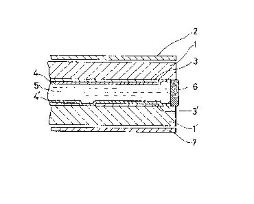
Rererring now to Fig.3 a linuid crystal dlsplaY
device in accor~ance with the Preserlt invention is
illus-trated -in a cross sectional view. The device
comPrises a Pair of glass subs-trates 2 and 2 a
rirst parallel electrode strips formed on the sub-
strate 2 and exten~ing in the lateral d-irection a
second parallel electrode striPs formed on the sub-
strate 2 and extenrling in the normal direction to
the plane of lhe dra~/ing sheet a first orientatlon
control Film 4 made of a Polyimide resin a second
orientation control film 4 made of SiO2 and an
ester -Ferroelectric liquid crYs-tal laYer 5. The ferro-
'PE~-29-09 18:53 KK ~ "-J~ "3 P.9
~3~
.
electric liquld crys~al material ls a comPoslte chlral
smect~c C Phase llqu~d crystal. The comblnation of
the first and second electrode striPS 3 and 3' con-
stitutes an electr~de arrangement ~n a matrix form
compr~s~ng a number of pixels. By appropriatelY
selectton oF a suitable resin to form the orlentatlon
control films, it is made Possible to relativelY rlse
the threshold level of the swltch~ng signa1s aPplied
to the llquid crystal laYer~ The first ~nd second
orientation control ~lms 4 and 4' are given rubbins
treatment, Assuming the scanning of the pixels is to
be carried out ~n the directlon Parallel to the first
electrode strips 3, the rubbing have to be performed
in the directlon normal to the Plane of the drawlng
sheet. In other words, rubblng is perfor,med along the
columns in case of desisns adapted for scanning along
the rows. The perlPherY of the substrates ls Provided
wlth a sealing member 6 for avoiding a loss of liquid
crystal, Reference numerals 1 and 7 deslgnate Polar
zlng plates arranged at the right directions. The
dimensions of parts of the device shown ln the flgure
are only chosen for illustration but not in accordance
with a real design. Although not shown in the flgure,
when assembled, spacers are interposed between the
substrates ln order to maintain the distance constant.
In realitY~ the d~stance between the substrate is 3
microns; the width of each electrode strip is 0.36 mm
and seParated from an ad~acent str~p by 0.04 ~m
intervals.
7 `~tJ!
'~18-l~9-~39 19:55 K~< J~ J~,-t"-'J~ "3 P.10
~3317
Particularly, ~n accordance with the present
inventlon~ ~he l~quid crYstal mater~al is prepared ln
order to have a broad transltlon range wlthin whlch
the phase of the llqu~d crysta~ ~s graduallY chansed
from lts ~sotropic Phase to its ~uasl-crYstalline
phase. In order to obtaln such a transition characte-
ristic~ the llquid crystal matertal is Prepared bY
blending several k~nds of liquld crystals. The liqu~d
crystal constituents are selected from those having
d~verse transltlon temPeratures distr~buted over a
wlde temperature ranse. We have ob~ained a comPosite
llquid crystal mater~al having a wide transition
temPerature range bY blending eight klnds of llquid
crYstal esters.
What follow are e~ght l~quid crystal const~-
tuents with respective Proportion ~n parenthesis
which constitute a comPoslte liquid crYstal in accor~
dance with the Present invention.
NO 1 C8Hl7 ~ -C02 ~ C02 ~
Cryst<-(31.8~C)-~Smc1~<-(32.6C)-~Sm~-(53.0~C)->Iso
NO 2~ ClOH21 ~ C02 ~ COz ~
Cryst<-(42.fi~C)-~Smc~<-(43.8C)->SmAc-(54.2~C)->Iso
8 ~.
9-09 1 ~1: 56 Kl< ~ j" 3 P . 1 1
3~
N0, 3: C8Hl 70~C02~0/~\
( 3 0 . 7 % )
Cryst<-(47.3C)->Smc~<~(47.80C) >SmA<-(~8.7C)->lso
N0;4~ C8Hl70~C02~C02/~\
Cryst<-(75,9C)->Srn~*<-(136,3C)->SmA<-(162.2C)->lso
N0 ~ ~ C l o H 2 l ~ C 0 z ~ C 2 /~/
Cryst~-(6l .5~C)~>Smc~-( l40.7C)->SmA<-( 164.3C)-~Iso
o
N0 . 6: C~H170 ~C2 {C~/
(0.5%)
Cryst~-(83,3OC)->Smc~<-( l39~7C)->SmA<-( 152.4C)->lso
O
N0 . 7 ~ C 8 H l 7 ~ C 2 ~
Cryst<-(102.0C)~>Smc~<~ 2.0C)-~SmA<-(137~C) >Iso
N0 . 8: Cl oH2 1 o~C2 ~ /\
( 9 . 7 % )
cryst<-(27,0c)->sinc~<-(2g.3c) >SmA<-(55.0C)->Iso
9 , ~
'BEI-09-09 lE3:5E3 KK J~ L~JI,~ "3 P.lZ
~ 7
By b1ending the above constituents, a liquid
crystal material was obta~ned wlth ~ts trans~t~on
characterlstlcs such that Crystal~-(4.7C-3.5~C)->
S~ <-( 62.5C-51 .9C)->SmA<-(B9.7C-75 .4C)-~Iso
It w~ll be not difficult for those skilled in
the art to prepare liqu~d crystal mater~als whlch
have transitlon characteristlcs suitable to the ap-
plications. In accordance with exPerlmental, we pre-
pared another liquld crYstal mater~al whose Phase
transltion was such that lsotroplc liqu~d ~- (130C -
98C) -> smectic A <- (73C - 60C) -> smectic ~C <-
(10C - 0C) -> smect~c ~I <- (-10C) -> crystal.
After lnterpos~ng such a comPosite llquid crystal
materlal between the or~entatlon control films pro-
vided on the substrates 2 and 2' at a temPerature at
whlch the liqu~d crYstal material is in its isotropic
phase, the structure is graduallY cooled to a te~Pe-
rature at which the entlretY of the composite liquld
crystal mater~al ~s in its smectic Phase. By the
way, liquid crystal molecules form micro-doma~ns
whlch grow as the temPerature r~ses. Each micro-
domain can be regarded to have a quasi-monocrYsta
11ne structure. The proport~on of each constltuent
be~ng 5-20%. It w~ll be deslre~ ~n general to l~m~t
the max~mum proportion of the constltuents up to 20
and to use many k~nds of liquld crystals at nearly
equal proportlons resPectlvelY~ The ~ormation of
micro-domalns in the l~quld crystal layer starts
;,,`~i
09-09 18:59 KK ~ $'~:J"3 P. 13
~ 31"~
along the oriented surface given rubbing treatment so
that the quas~-polycrystall~ne area conslst-lns o~
m~cro-domains gradua17y grows as the temPerature
rlses. ~ig~4 shows a sketch topologically drafted ln
accordance with a m~croscoPic photograPh of the micro-
domains. The w~dth and the length of each m~cro-
domaln 8 are about several microns and several hund-
reds microns respectlvelY~ The signif~cant feature of
the structure co~prising the micro-domalns is the
absence of z~-zag defects. While the interfaces 9
between the micro-domains 8 are defects, the entirety
of the liquid crystal can be regarded approximatelY
as a uniform ~uasi-crystalline structure except for
the lnterfaces between the domalns which are small
defects.
When a sawtooth pulse hav~ng a ~aximum voltage
of ilOV ls applled between the electrode striPs 3 and
31, the molecular state of the p-ixel iust sandwlched
bY the activated two electrodes is chan~ed. The state
change takes place uniformly ln every mlcro-domaln 8
wtthin the plxel so that the entirety of the pixel is
changed at once. In accordancc with exPer~mental,
there was observed no dlfference in the chang~ng pro-
cess between a central position and a Prepheral P~si~
tion o~ the pixel.
Figs.5(A) and 5(B) are microscopic Photosraphs
showlng mlcro-domains taken at two sites of a liqu~d
crystal layer 1n smectic A ln accordance wlth the
present inventlon with ~agniflcat~on of ~OO bY use o~
11 ~i
'8E3--09--09 1~:01 KK J~ y~I~J~-t"--'J~ j"3 P.14
polarizlns Plates which are arranged normal to each
other and suppor~lng the liquld crystal therebetween.
The distance between a pair Gf substrates was selec-
ted to be 20 microns rather than 3 mlcrons for tak~ng
photosraPhs ln wh~ch mlcro-domain textures aPpear
clearlY~ As shown in the Photographs~ the llquid
crystal is devided ~nto a number of mlcro-domalns.
Thls ~eans that llquicl crystal molecules have been
oriented unlformly in each micro-domaln but adiacent
mlcro-domains have been orlented in different orien-
tat~on dlrectlons. The micro-doma~ns have several
m1crons in wldth and several hundreds microns in
length. The m~cro-domains are formed aPProxlmately
Parallel to the rubblng direct~on given to the orien-
tati~n control films.
As the phase of llquld crystal ls transformed to
smect~c C at a descended kemperature, strlpes appear
in each micro-do~aln as seen from Figs.6(A) and 6(B)
~aken in the same conditlon as F~gs.5(A) and 5(B)
except for khe temPerature. The wldth of each str~pe
corresponds to one turn of a hellx of the chiral
smectic C liqu~d crYstal and ls about 3 microns. As
shown ln the photographs, strlPes of neishbourlns
mlcro-doma~ns are aligned at the ~nter~aces. ~gs,
7(A) and 7(B) are photograPhs in the case that the
dlstance between the substra~es ls about 3 m~crons,
other condltions be~ng same as Flgs.5(A~ and 5(B).
The length o~ each mlcro-domalns become short as com-
pared wlth Fl~s,6(A) and 6(B). Such a narrow dlstance
12 ~
~333 ~
be-tween the substrates allows the liquid crystal helices unwin-
ded, and therefore the response speed becomes as fast as 10
microseconds when measured ln the same conditlon as the case of
20 microns.
While several embodiments have been specifically des-
cribed, it is to be appreciated that the present invention is not
limited -to the particular examples described and that modifica-
tions and variations can be made without departure from the scope
of the invention.