Note: Descriptions are shown in the official language in which they were submitted.
1~9~
SPECIFICATION
DISCHARGE LAMP DRIVING CIRCUIT
BACKGROUND OF THE INVENTION
1. Field of the Invention
The present invention is directed to a discharge lamp
driving circuit, and more particularly to a circuit for
operating a high-pressure gaseous discharge lamp without
causing a harmful acoustic resonance.
2. Description of the Prior Art
There has been a growing demand for a discharge lamp
operating circuit which is operated at a higher frequency in
order to reduce the weight and bulk of the ballasting
inductor. On the other hand, it is also known that
discharge lamps, particularly high-pressure discharge lamps
such as mercury high pressure lamps and sodium vapor lamps
suffer from unstable discharge arcs due to "acoustic
resonance" when operated at certain high frequencies. U.S.
Pat. No. 4,291,254 proposed to select a stable frequency for
avoiding such "acoustic resonance". However, such stable
frequency is seen only in a limited range and differs from
different kinds of lamps, thus reducing the flexibility of
circuit design. Further, it is known that an extreme high
frequency drive, for example, over 100 KHz may be effective
for elimination of the "acoustic resonance", but this
eventually results in considerable switching losses and
d~
37~6
noises which are not acceptable for the lamp operation. To
this end, there has been proposed in Japanese Datent
Publication (KOKAI) No. 60-262392 to drive the lamp by a
composite lamp driving current having a repeating cycle of
an alternating current interrupted by a dc current. This
patent is based upon the finding that the repetitive
interruption of the alternating current by the dc current
can restrain the occurrence of the "acoustic resonance",
even the alternating current is in a frequency range which
would otherwise cause the "acoustic resonance". In this
sense, this patent is advantageous in selecting a lamp drive
frequency without having to consider the "acoustic
resonance". Notwithstanding this advantage, the patent has
a certain drawback in that two independent switching
circuits, i.e., chopper and inverter circuits, are required
for providing the dc current and the alternating current,
respectively. This requires duplication of switching
elements with consequent complexity in incorporating the
respective drivers in circuits for the duplicated switching
elements, thus eventually resulting in increased cost and
bulk of the physical circuit assembly.
SUMMARY OF THE INVENTION
The present invention eliminates the above problem by
commonly utilizing at least one switching element for
chopper and inverter switching circuits and provides an
~937~
improved discharge lamp driving circuit with simplified
circuit arrangement.
It is therefore a primary object of the present invention
to provide an improved discharge lamp driving circuit which
is simple in configuration, yet preventing the acoustic
resonance as well as assuring to make compact the physical
arrangement of the circuit.
An improved discharge lamp driving circuit in accordance
with the present invention comprises a dc (direct current)
voltage source, chopper means, and inverter means. The
chopper means comprises a first switching circuit which is
coupled to the dc voltage source to provide therefrom a
periodically interrupted current and smooth the same for
producing a smoothed dc current. The inverter means
comprises a second switching circuit which is also coupled
to the dc voltage source for producing therefrom a high
frequency alternating current. Included in the circuit is
control means which is connected to the chopper means and
the inverter means in order to apply to the discharge lamp a
repeating cycle of a composite lamp driving current composed
of the high frequency alternating current supplied from the
inverter means and is interrupted by the smoothed dc current
supplied from the chopper means.
A characterizing feature of the present invention resides
in that the first and second switching circuits of the
~Z937~`6
chopper and inverter means are arranged to have at least one
common switching element which operates both in producing
the dc current and the high frequency alternating current.
With this result, the circuit configuration can be
considerably simplified with consequent reduction in cost
and bulk of the device.
In a preferred embodiment, the chopper means is
configured in a bridge arrangement to apply to the discharge
lamp the smoothed dc current which is reversed in polarity
from one cycle to the subsequent cycle of the composite lamp
driving current. Thus, the deterioration of lamp electrodes
can be reduced to a minimum, thereby giving rise to an
enhanced life time of the discharge lamp.
The lamp driving circuit of the present invention can be
broadly classified into two types with and without a
transformer which operates to apply the high frequency
alternating current to the discharge lamp. In the former
type, the first switching circuit of the chopper means
comprises at least one switching element common to the
second switching circuit of the inverter means. The common
switching element is coupled in series circuit with an
inductor and a parallel combination of the discharge lamp
and a bypass capacitor of which series circuit is connected
across the dc voltage source. During a first period of
time, the common switching element is controlled to turn on
1~937~6
and off at a first high frequency to produce the interrupted
current which is smoothed by the first inductor and of which
high frequency component is bypassed through the bypass
capacitor for giving the smoothed dc current to the
discharge lamp within each cycle of the composite lamp
driving current. The second switching circuit of the
inverter means comprises a pair of first and second
switching elements at least one of which is common to the
first switching circuit of the chopper means. The first and
second switching elements are connected in series across the
dc voltage and is connected in circuit with a dc blocking
capacitor and the transformer with a primary winding and a
secondary winding which is inserted in series relation with
the discharge lamp and in parallel relation with the bypass
capacitor. The blocking capacitor is connected in series
with the primary winding of the transformer and in parallel
with one of the first and second switching elements to form
therewith a series oscillating circuit. During a second
period of time alternating with the above first period of
time, the first and second switching elements are controlled
to alternately turn on and off at a second frequency to
provide a high frequency alternating current in the series
oscillating circuit as repeating to charge and discharge the
dc blocking capacitor, whereby inducing the corresponding
high frequency alternating current in the circuit of the
12937~6
- 6 -
secondary winding and the discharge lamp to drive the
discharge lamp by such high frequency alternating current
within each cycle of the composite lamp driving current.
In the other type of the circuit without the transformer,
the first and second switching circuits of the chopper and
inverter means commonly includes a pair of first and second
switching elements arranged in a half- or full-bridge
configuration with a pair of capacitors or with a pair of
like switching elements. The bridge has its input ends
connected across the dc voltage source and has its output
ends connected across a series circuit composed of an
inductor and a parallel combination of the discharge lamp
and a bypass capacitor. During a first period of time, one
of the first and second switching elements is controlled to
turn on and off at a first frequency with the other
switching element being kept turned off to provide a dc
current which is smoothed by the inductor and is removed of
its high frequency component by the bypass capacitor for
feeding the smoothed dc current to the discharge lamp within
each cycle of the composite lamp driving current. During a
second period of time alternating with the first period of
time, the first and second switching elements are controlled
to a~ternately turned on and off at a second high frequency
in such a manner as to provide to the discharge lamp said
high frequency alternating current within each cycle of said
1~29;~7~6
composite lamp driving current. The second high frequency
is determined to be lower than the first high frequency to
such an extent that the second high frequency alternating
current is supplied to the discharge lamp within each cycle
of the composite lamp driving current while allowing the
second high frequency component to be substantially fed to
the discharge lamp without being bypassed through the bypass
capacitor.
BRIEF DESCRIPTION OF THE DRAWINGS
FIG. 1 is a schematic diagram of a discharge lamp driving
circuit illustrating one basic version in accordance with
the principle of the present invention;
FIG. 2 is a waveform chart illustrating a composite lamp
driving current in a conceptual form obtained in the present
invention;
FIG. 3 is a circuit diagram of a discharge lamp driving
circuit in accordance with a first embodiment of the present
invention;
FIG. 4 is a timing diagram of waveforms illustrating the
operation of the two switching transistors shown in FIG. 3;
FIG. 5 is a waveform chart illustrating a composite lamp
driving current in a conceptual form obtained in the circuit
of FIG. 3;
FIG. 6 is a circuit diagram of a modification of FIG. 3;
~937f~
- 8 -
FIG. 7 is a circuit diagram of a second embodiment of the
present invention;
FIG. 8 is a timing diagram of waveforms illustrating the
operation of the four switching transistors shown in FIG. 7
FIG. 9 is a timing diagram of waveforms illustrating another
operation of the four switching transistors shown in FIG. 7
in accordance with a modification of the second embodiment;
FIG. 10 is a waveform chart illustrating a lamp driving
current in a conceptual form obtained by the switching
operation of FIG. 9;
FIG. 11 is a circuit diagram of a third embodiment of the
present invention;
FIG. 12 is a timing diagram of waveforms illustrating the
operation of the four switching transistors shown in FIG.
11;
FIG. 13 is a timing diagram of waveforms illustrating
another operation of the four switching transistors shown in
FIG. 11 in accordance with a modification of the third
embodiment;
FIG. 14 is a circuit diagram of a fourth embodiment of the
present invention;
FIG. 15 is a timing diagram of waveforms illustrating the
operation of the two switching transistors shown in FIG. 19;
FIG. 16 is a waveform chart illustrating a composite lamp
driving current in a conceptual form obtained by the
~937~6
g
switching operation of FIG. 15;
FIG. 17 is a circuit diagram of a fifth embodiment of the
present inventioni
FIG. 18 is a timing diagram of waveforms illustrating the
operation of the three switching transistors shown in FIG.
17;
FIG. 19 is a circuit diagram of a sixth embodiment of the
present invention;
FIG. 20 is a timing diagram of waveforms illustrating the
operation of the two switching transistors shown in FIG. 19;
FIG. 21 is a circuit diagram of a seventh embodiment of the
present invention;
FIG. 22 is a circuit diagram of an eighth embodiment of the
present invention;
lS FIG. 23 is a timing diagram of waveforms illustrating the
operation of the two switching transistors shown in FIG. 22;
FIG. 24 is a circuit diagram of a ninth embodiment of the
present invention;
FIG. 25 is a circuit diagram of a tenth embodiment of the
present invention:
FIG. 26 is a timing diagram of waveforms illustrating the
operation of the four switching transistors shown in FIG.
25; and
FIG. 27 is a timing diagram of waveforms illustrating
2S another operation of the four switching transistors shown in
1~93~
- 10 -
FIG. 25 in accordance with a modification of the tenth
embodiment.
DETAILED DESCRIPTION OF THE PREFERRED EMBODIMENTS
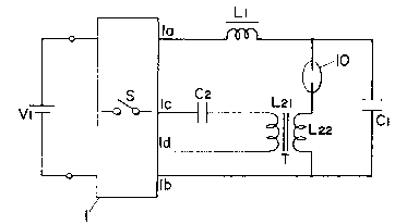
Referring now to FIG. 1, one version of a discharge lamp
driving circuit in accordance with the present invention is
shown in a general form for easy understanding of the
principle of the present invention. The circuit comprises a
switching section 1 which is connected across a dc voltage
source V1 and includes at least two switching elements or
transistors collectively indicated in FIG. 1 as S. The
switching section 1 has a first pair of output ends la and
lb between which is connected a series circuit of an
inductor L1 and a parallel combination of a discharge lamp
10 and a bypass capacitor C1. Also provided at the
switching section 1 is a second pair of output ends lc and
ld between which is connected a circuit of a dc blocking
capacitor C2 and a transformer T with a primary winding L
and a secondary winding L22. The secondary winding L22 is
coupled in series with the discharge lamp 10 in parallel
relation with the bypass capacitor C1. Tne switching
section 1 is controlled, during a first period of time T~
(t1 - t2), to repetitively interrupt the dc voltage at a
first high frequency for providing a chopped voltage between
the first pair of output ends la and lb. The chopped
voltage is then smoothed by the inductor L1 and has its high
1~937~
frequency component bypassed through the bypass capacitor C
to thereby feed a smoothed dc current I~ to the discharge
lamp 10 during the first period TDC~ as shown in FIG. 2 which
shows a composite lamp driving current Ia in a conceptual
waveform. During a second period of time T~ (t2 - t3)
alternating with the first period of time T~, the switching
section 1 is controlled to repetitively interrupt the dc
voltage at a second high frequency in order to repeat
producing a voltage between output ends le and ld and
shorting the same. While the positive voltage is developed
across the output ends le and ld, the voltage is applied
through the dc blocking capacitor C2 to the primary winding
L2l of the transformer T so as to flow a current in one
direction in the primary winding Lzl as charging the blocking
capacitor C2. Upon subsequent shorting between the output
ends le and ld, the blocking capacitor C2 discharges to feed
an opposite current through the primary winding L21.
Consequently, the above repetition of developing the voltage
and shorting between the output ends le and ld will induce
an alternating current with the second high frequency at the
secondary winding L22 of the transformer T such that the
resulting high frequency alternating current is caused to
circulate through the closed loop of the lamp 10 and the
bypass capacitor Cl as it is blocked by the inductor L1,
whereby providing to the lamp the high frequency alternating
~;~93~
- 12 -
current IAC during the second period of time T~, as shown in
FIG. 2. In this manner, the switching section 1 provides a
repeated cycle of a composite lamp driving current composed
of the high frequency alternating current I~c interrupted by
the dc current IDC. With this result, the lamp 10 can be
kept free from causing an acoustic resonance or instable
lamp operation even if the alternating current has a high
frequency which might cause such acoustic resonance when
utilized alone. The second frequency of the alternating
lamp current may be suitably selected to be equal to or
different from the first frequency at which the switching
section 1 is operated to chop the dc voltage. With the
circuit arrangement of FIG. 1, it is possible to share at
least one switching element in the switching section 1 which
operates both in a chopper mode for providing the dc current
I~ and in an inverter mode of providing the high frequency
alternating current I~. It is also noted in this connection
that other components can be commonly and effectively
utilized in the above two different operation modes. For
example, the bypass capacitor Cl, which acts to bypass the
high frequency component of the dc current in the chopper
mode, serves to complete the closed loop with the secondary
winding L22 and the discharge lamp 10 to effectively apply to
the discharge lamp 10 the alternating voltage developed at
the secondary winding L22 in the inverter mode. Also the
1~937
- 13 -
inductor L1, which smoothes the chopped voltage in the
chopper mode, serves to block the high frequency voltage and
prevent it from being applying to tne circuit other than the
closed loop, thereby applying the high frequency voltage
effectively to the discharge lamp 10 in the inverter mode.
Further, the secondary winding L22 of the transformer T,
which develops the high frequency voltage as a power source
in the inverter mode, can serve to block the high frequency
component of the chopped voltage in the chopper mode,
assisting to bypass the high frequency component through the
bypass capacitor Cl. The discharge lamp 10 may be a high
pressure gaseous discharge lamp such as mercury high
pressure discharge lamp with metal halogen additives, sodium
vapor lamp, and the like, or may be a low pressure lamp.
The present invention is now discussed in more detail
with reference to preferred embodiments. Like numerals
designate like parts throughout the following embodiments
for easy reference.
First embodiment <FIGS. 3 to 5>
In this embodiment, the circuit comprises a pair of first
and second switching transistors Q1 and Q2 which are
cooperative with a pair of capacitors Q3 and Q, to form a
half-bridge having its input ends connected across a dc
voltage source V,. Connected across the output ends of the
half-bridge is a series circuit composed of an inductor L1
~937~
- 14 -
and the parallel combination of a discharge lamp 10 and a
bypass capacitor C1. The first and second switching
transistors Q1 and Q2 are cooperative with the series circuit
to form a chopper which provides a dc current to the
discharge lamp 10. A transformer T is incorporated in the
circuit with its primary winding L21 connected in series with
a dc blocking capacitor C2 across the second switching
transistor Q2 and with its secondary winding L22 inserted in
series with discharge lamp 10 and in parallel with the
bypass capacitor C1. The series connection of the primary
winding L21 and the blocking capacitor C2 is cooperative with
the first and second switching transistors Q1 and Q2 to form
an inverter or series oscillating circuit which provides a
high frequency alternating current to the discharge lamp 10.
As discussed in the below, the first and second switching
transistors Q1 and Q2 are controlled to provide repeating
eyeles of a composite lamp driving current composed of the
dc current fed from the chopper and the high frequency
alternating current from the inverter, as shown in FIG. 5.
Typical values for the above circuit are as follows. The
voltage of the dc voltage source V1 is 280 V, the bypass
capacitor C1 has a capacitance of 0.22 ~F, the inductor L,
has an inductance of 0.2 mH, the primary winding L21 has an
inductance of 0.5 mH, and the blocking capacitor C2 has a
capacitance of 0.1 ,uF. The first and second switching
1~937~i
- 15 -
transistors Q1 and Q2 are operated at 90 KHz both in the
chopper and the inverter mode. The operation of the chopper
is now explained with reference to FIG. 9. During each
first period of time T~ alternating with a second period of
time T~, one of the first and second switching transistors
Ql and Q2 is controlled to turn on and off at a first high
frequency while the other switching transistor is kept
turned off. For example, during the first period of time T~
(tl - t2) of FIGS. 4 and 5, the first switching transistor Ql
repeats turning on and off at a frequency of 40 KHz while
the second transistor Q2 is kept turned off. When the first
transistor Q1 is on, the capacitor C3 will discharge a
current through a route of the first switching transistor
Ql, secondary winding L22, discharge lamp 10, and inductor Ll.
When the first transistor Ql is turned off, the inductor Ll
acts to continuously flow the current in the same direction.
Thus, the dc current from the capacitor C3 iS smoothed by
the inductor Ll and has its high frequency component
bypassed through the bypass capacitor Cl so as to feed the
smoothed dc current to the discharge lamp 10. During the
first period of time Tw (t3 - t,), the second switching
transistor Q2 turns on and off at the same frequency while
the first switching transistor Ql is kept turned off,
thereby producing the like dc current but in opposite
polarity, as shown in FIG. 5. With this provision of
1~937~
- 16 -
reversing the polarity of the dc current from one cycle to
the subsequent cycle of the composite lamp driving current,
the discharge lamp 10 can have an elongated operation life.
The second period of time T~ in which the inverter is
active to provide the high frequency alternating current is
initiated by driving to turn on and off the one of the
switching transistor which is kept turned off in the
previous first time of period while keeping the other
switching transistor turning on and off. For example, in
the second period of time T~ (t2 - t3), the second switching
transistor Q2, which has been off in the previous first time
of period T~, begins to turn on and off while the first
switching transistor Ql continues to turn on and off.
During this period, the first and second switching
transistors Q1 and Q2 are alternately turned on and off with
a dead-time therebetween, in which both of the switching
transistors are simultaneously off, in order to provide the
high frequency alternating current. The inverter operation
in this period is explained in terms of the repeating
~0 sequence of the following four consecutive occurrences 1) to
4), as indicated in FIG. 4.
At the first occurrence 1), the second switching transistor
Q2 is turned on while the first switching transistor Ql is
off such that the blocking capacitor C2 which has been
charged due to the previous turning on of first switching
~937~
- 17 -
transistor Ql will begin discharging to cause a current toflow through the primary winding L2" second switching
transistor Q2, and back to the blocking capacitor C2. At the
second occurrence 2) in which both of the first and second
switching transistors Q, and Q2 are off, the primary winding
L2l in turn causes the current to continuously flow through a
first diode Dl, dc voltage source V1, blocking capacitor Cz
and back to the primary winding L21. At the third occurrence
3), the first switching transistor Ql is on while the second
switching transistor Q2 is off so that the capacitor C3
discharges its energy, causing a current to flow in the
opposite direction through the first switching transistor
Ql, primary winding L21, blocking capacitor C2, capacitor C"
and back to the capacitor C3 . At the fourth occurrence 4)
where both of the first and second switching transistors Ql
and Q2 are off, the primary winding L2, acts to continuously
flow the current through a second diode D2, blocking
capacitor C2, and back to the primary winding L2l. In this
sense, the first and second diodes D1 and D2, which are
connected in antiparallel relation respectively to the first
and second switching transistors Q1 and Q2, provide first and
second bypass routes for continuously flowing the
instantaneous currents discharged from the primary winding
L2l at the second and fourth occurrences in which both of the
switching transistors Q1 and Q2 are off.
129;~7~6
- l& -
Likewise, in the next second period of time T~ (t, - t5)
which is initiated by turning on and off the first switching
transistor Ql which has been on in the previous first time
of period T~, the first and second switching transistors Q
S and Q2 are controlled to alternately turn on and off to
produce the high alternating current through the primary
winding LZ1-
In this manner, during each second period of time T~, the
high frequency alternating current continues to flow through
the primary winding L2l to thereby induce at the secondary
winding L22 the corresponding high frequency alternating
current which circulates through the closed loop of the
secondary winding L22, discharge lamp 10, and the bypass
capacitor C1 as the inductor L1 acts to block such high
lS frequency alternating current, whereby driving the discharge
lamp 10 by thus obtained high frequency alternating current,
as shown in ~IG. 5.
It is noted at this connection that the second frequency
is determined so that the inductor L1 blocks such high
frequency for circulating the high frequency alternating
current through the closed loop of the secondary winding L22,
discharge lamp 10, and bypass capacitor Cl. Due to the
above the circuit arrangement, the first and second
switching transistors are commonly utilized both in the
chopper mode of providing the dc current and in the i.nverter
~2937f.~
- 19 -
mode of providing the high frequency alternating current to
the discharge lamp. In brief, the inverter mode of
providing the high frequency alternating current is
terminated by deactivating one of the switching transistors,
which in turn immediately initiates the ehopper mode of
providing the de eurrent to the discharge lamp. Thus, by
repeating the above operations, the high frequeney
alternating eurrent can be repetitively interrupted by the
de eurrent, as shown in FIG. 5, to thereby inhibit the
oeeurrenee of the aeoustie resonanee whieh would be
otherwise develop due to the high frequency lamp driving.
The ratio of the period TDC to the period of one complete
eyele (T~ + T~) of the composite lamp driving current may be
suitably selected depending upon the kind of discharge lamp
utilized for prevention of the acoustic resonanee, as the
suitable ratio will vary with different kinds of lamps.
Modifieation of the first embodiment <FIG. 6>
This modifieation shows a eireuit arrangement whieh is
identieal to that of FIG. 3 exeept that the dc bloeking
eapaeitor C2 is inserted between the primary winding L21 and
the eonneetion of the eapaeitors C3 and C,. The eireuit
provides the like eomposite lamp driving current of FIG. 5
by the like switehing operations of FIG. 4, but in whieh
eaeh of the eapacitors Q3 and Q, is additive to the blocking
eapacitor C2 to act as a voltage source to provide the high
~Z937t~
-- 20 --
frequency alternating current during the second period of
time T~. The other functions are identical to those of the
first embodiment. In other words, during the second period
of time for providing the high alternating current, the
S capacitors Q3 and Q, can be made mainly responsible for
producing the high frequency alternating current, while the
blocking capacitor C2 is responsible for blocking the dc
current. Accordingly, the constant of the blocking
capacitor C2 can be determined relatively freely without
taking into account for utilizing it as the voltage source
for the alternating current, thus giving rise to an improved
design flexibility of the circuit. Typical values for this
circuit when operated on the dc voltage Vl of 280 V are as
follows. Cl = 0.22 ,uF, L, = 0.22 mH, L21 = 0.9 mH, and C2 =
0.01 uF. The first and second switching transistors Ql and
Q2 are operated at 40 KHz and 60 KHz, respectively in the
chopper mode and the inverter mode.
Second embodiment <FIGS. 7 and 8>
Referring to FIG. 7, a second embodiment of the present
invention is shown to be identical to the first embodiment
of FIG. 3 except for utilizing additional third and fourth
switching transistors Q3 and Q, which are coupled with the
first and second switching transistors Ql and Q2 to form a
chopper circuit of full-bridge configuration with third and
fourth diodes D3 and D, connected in antiparallel relation to
1'~937~;
the third and fourth switching transistors Q3 and Q"
respectively. Thus, as shown in FIG. 8, the one of the two
diagonally disposed pairs of switching transistors Ql, Q"
and Q2, Q3 is rendered to be active while the other pair is
inactive during the first period of time T~ providing the dc
current to the discharge lamp 10. For example, during the
first period of time T~ (t1 - t2), the first switching
transistor Ql is controlled to turn on and off at a first
high frequency with the fourth switching transistor Q, being
kept turned on, while the second and third switching
transistors Q2 and Q, are kept turned off. In this manner
the switching transistors are controlled to provide the dc
lamp current which is opposite in polarity from the period
tl- t2 to the period t3 - t,. In the inverter mode of
providing the high frequency alternating current, or in the
second period of time T~ (t2 - t3, t, -t5), the first and
second switching transistors Q1 and Q2 are controlled in the
same manner as in the first embodiment while the third and
fourth switching transistors Q3 and Q, are kept turned off,
during which the first and second switching transistors Ql
and Q2 are cooperative with the primary winding L2, and the
blocking capacitor C2 to oscillate an al~ernating current
through the primary winding L2l and the hlocking capacitor
C2, as repeating the four occurrences which are similar to
those discussed with reference to the first embodiment but
~9~76~
- 22 -
differ in that the dc voltage Vl will supply an energy to
the series oscillating circuit of the primary winding L2l and
the blocking capacitor C2 when the first switching
transistor Ql is on and the second switching transistor Q2 is
off.
Modification of the second embodiment <FIGS. 9 and 10>
The modification of the second embodiment utilizes the
same circuit arrangement of FIG. 7, but operates the first
and second switching transistors Ql and Q2 as shown by the
timing diagram of FIG. 9. As seen from FIG. 9, in the
chopper mode of providing the dc current during the first
period of time T~c (tl - t2, t3 - t~), both of the first and
second switching transistors Ql and Q2 are operative to
alternately turn on and off such that during this period TDC
the discharge lamp 10 receives, in addition to the smoothed
dc voltage from the dc voltage source Vl, the induced
voltage developed at the transformer T due to the
oscillation in the circuit of the primary windi.ng L2~ and the
blocking capacitor C2. Thus, the resulting dc lamp current
may take the form of FIG. lO in which the high frequency
component is superimposed on the smoothed dc current (tl -
t2, t3 - t,).
Third embodiment <FIG. 11 and 12>
Referring to FIGS. 11 and 12, a third embodiment of the
present invention is shown to comprise the same like circuit
1~937~
- 23 -
as in the second embodiment except that the blocking
capacitor C2 has its one end connected to the connection
between the third and fourth switching transistors Q3 and Q4.
The switching transistors Ql to Q, are controlled to turned
on and off in accordance with a timing diagram of FIG. 12 to
provide the like composlte lamp driving current as shown in
FIG. S for the first embodiment. In the chopper mode, the
two diagonally disposed switching transistors, for example,
Ql and Q" are controlled to turn on and off in a
synchronized manner while the other two switching
transistors, for example, Q2 and Q3 are kept turned off
during each first period of time T~ in order to provide the
dc current to the discharge lamp 10. Due to the synchronous
operation of the diagonally disposed switching transistors
Ql, Q, and Q2, Q3 in the chopper mode, the inductor Ll acts
upon the subsequent turning off of the all switching
transistors to cause the instantaneous dc current to
continuously flow through a closed loop to the dc voltage
supply Vl, thus feeding ~ack the energy thereto. For
example, when all of the switching transistors are turned
off immediately after the first and fourth switching
transistors Q1 and Q, being turned on, the inductor Ll cause
the current to flow through the diode D3, dc voltage source
Vl, diode D2, secondary winding L22, discharge lamp 10 and
back to the inductor L2l. On the other hand when all the
1~937~6
- 24 -
switching transistors are turned off after the second and
third switching transistors Q2 and Q3 being simultaneously
turned on, the instantaneous current from the inductor L21
flows through the discharge lamp lO, the secondary winding
S L22, diode Dl, dc voltage source, diode D" and back to the
inductor ~21'
In the inverter mode of providing the high frequency
alternating current during the second period of time T~
(t2 - t3, t~ - tS), the two switching transistors, for
example, Ql and Q, in one diagonally disposed pair are
controlled to simultaneously turn on and off while the
switching transistors Q2 and Q3 in the other pair are
controlled to simultaneously turn on and off in an
alternating manner therewith. Thus, the alternating current
appears in the series oscillating circuit including the
primary winding L2, and the blocking capacitor C2 with no
substantial direct current being caused to flow through the
discharge lamp 10 and the inductor L" whereby inducing at
the secondary winding L22 the high frequency alternating
current which circulates the closed loop of the secondary
winding L22, discharge lamp 10, and bypass capacitor C1.
Also in the inverter mode, when all the switching
transistors are simultaneously turned off, the primary
winding L2l acts to fed back its accumulated energy to the dc
voltage V1 through the diodes D3 and D2 or the diodes D1 and
~Z93766
D~.
Modification of the third embodiment <FIG. 13>
A modification of the third embodiment utilizes the same
circuit of FIG. 11 but in which the switching transistors Q
S to Q, are controlled in a somewhat different manner from the
third embodiment. As shown in FIG. 13, the difference is
seen in that, during first period of time T~ (chopper mode),
the first switching transistor Q1 is controlled to turn on
and off while the fourth switching transistor Q, is kept
turned on (tl - t2), and the third switching transistor Q3 is
controlled to turn on and off while the second switching
transistor Q2 is on (t3 - t,). Thus, upon the turning off of
the first switching transistor Ql, the switching transistor
Q, is cooperative to the diode D2 to form a closed loop
including the inductor Ll for circulating therethrough the
current which is otherwise fed back to the dc voltage source
V1 through the diodes D3 and D2 as seen in the third
embodiment. Likewise, upon turning off of the third
switching transistor Q3, the second switching transistor Q2
is cooperative with the diode D, to circulate the current
which is otherwise fed to the dc voltage source Vl through
the diodes Dl and D~ as seen in the third embodiment.
Fourth embodiment <FIGS. 14 to 16>
A fourth embodiment of the present invention comprises
first and second switching transistors Ql and Q2 connected
across the dc voltage source Vl with first and second diodes
lZ937~6
- 26 -
Dl and D2 connected in antiparallel respectively with the
first and second switching transistors Q, and Q2- The
inductor L1 is connected in series with a parallel
combination of the discharge lamp 10 and bypass capacitor
C" which series-parallel combination is connected in
parallel with the second switching transistor Q2. Also
included in the circuit is the transformer T of which
primary winding L2, is connected in series with the dc
blocking capacitor C2 across the second switching transistor
Q2- The secondary winding L22 is inserted in series with the
discharge lamp 10 in parallel with the bypass capacitor C,.
In this circuit, the chopper is defined by the first
switching transistor Q" and the series-parallel combination
of the inductor Ll, discharge lamp 10, bypass capacitor C1,
as enclosed in dotted lines CH in FIG. 14. Also, as
enclosed in phantom lines IV in the figure, the inverter is
defined by, in additions to the above components common the
to the chopper, the second switching transistor Q2 and the
series circuit of the primary winding L2, and the blocking
capacitor C2, and the secondary winding L22.
In operation, the first and second switching transistors
Ql and Q2 are controlled in a manner as shown in FIG. 15 to
provide a composite lamp driving current of FIG. 16. That
is, in the chopper mode during the first period of time T~
(tl - t2 and t3 - t,), the first switching transistor Q1 is
1~93~7~
- 27 -
driven to turn on and off at a first high frequency to
provide to the -hopped dc voltage which is smoothed by the
inductor Ll and of which high frequency component is
bypassed through the bypass capacitor Cl to flow the
resulting smoothed dc current to the discharge lamp 10. In
the inverter mode during the second period of time T~ (t2 -
t3), the first and second switching transistors Q1 and Q2 are
driven to alternately turn on and off with a dead-time
therebetween at a second high frequency, which may be equal
to or different from the first high frequency, to cause an
oscillating current through the circuit of the primary
winding L21 and the blocking capacitor C2 as repeating to
charge and discharge the blocking capacitor C2 in the same
manner as effected in the previous embodiments. Thus, there
is developed at the secondary winding L22 the induced current
which will circulate through the closed loop of the
secondary winding L22, discharge lamp 10, and the bypass
capacitor Cl as the inductor L1 acts to block such high
frequency alternating current. In the inverter mode, the
current flowing to the inductor L~ is kept at a minimum by
suitably selecting the values for the inductor L~, bypass
capacitor C~, the secondary winding L22, and the driving
frequency or the second frequency at which the first and
second switching transistors Ql and Q2 are operated.
1~37~6
- 28 -
Fifth embodiment <FIGS. 17 to 19>
The discharge lamp driving circuit comprises the first
and second switching transistors Ql and Q2 connected across
the dc voltage source Vl with first and second diodes Dl and
D2 connected in antiparallel relation respectively to the
first and second switching transistors Ql and Q2. A third
switching transistor Q3 is connected in series with the
inductor Ll and the parallel combination of the discharge
lamp 10 and the bypass capacitor Cl across the first
switching transistor Ql- The transformer T is connected in
circuit with its primary winding L2, connected in series with
the blocking capacitor C2 across the second switching
transistor Q2 and with its secondary winding L22 inserted in
series with the discharge lamp 10 and in parallel with the
bypass capacitor Cl. In this embodiment, the chopper is
defined by the second and third switching transistors Q2 and
Q3~ the series-parallel circuit of inductor L1, discharge
lamp 10 and bypass capacitor Cl, as enclosed in the dotted
lines CH in FIG. 17, while the inverter is defined by, in
addition to the second switching transistor Q2, the parallel
combination of discharge lamp 10 and bypass capacitor Cl
common to the chopper, the transformer T and the blocking
capacitor C2, as enclosed in phantom lines IV in the figure.
These switching transistors Ql, Q2, and Q3 are controlled in
accordance with a timing chart of FIG. 18 so as to provide
1~93~7~
- 29 -
the like composite lamp driving current as seen shown in
FIG. 16 of the fourth embodiment. That is, in the chopper
mode during the period T~ (tl - t2 and t3 - t,), the second
switching transistor Q2 is driven to turn on and off at a
first high frequency while the first and third switching
transistors Q1 and Q3 are turned off and on, respectively,
whereby providing the smoothed dc current to the discharge
lamp 10 in the same manner as in the fourth embodiment. In
the inverter mode during the period T~ (t2 - t3), the first
and second switching transistors Ql and Q2 are driven to
alternately turned on and off with a dead-time therebetween
at a second high frequency which may be equal to or
different from the first high frequency, in order to produce
an high frequency alternating current through the primary
winding L2l and consequently circulate the resulting high
frequency alternating current through the closed loop of
secondary winding L22, discharge lamp 10, and bypass
capacitor Cl, in the same manner as seen in the previous
fourth embodiment. In the inverter mode, the third
switching transistor Q3 is kept turned off so that the
discharge lamp 10 will not receive the current directly from
the blocking capacitor C2 or from the dc voltage source Vl.
Sixth embodiment <FIGS. 19 and 20>
Referring to FIG. 19, a sixth embodiment of the present
invention is shown to comprises the first and second
lZ937C~6
- 30 -
switching transistors Ql and Q2 which are coupled with a pair
of capacitors Q3 and Q, in a half-bridge configuration having
its input ends connected across the dc voltage source V1.
First and second diodes D~ and D2a are connected in
antiparallel relation to the first and second switching
transistors Ql and Q2, respectively. Included in the circuit
is a diode network composed of a series combination of
diodes Dl1 and Dlz and another series combination of diodes D
and D22. These series combinations are connected in parallel
with one another between the first and second switching
transistors Ql and Q2. Another first diode Dl~ is connected
in series with diode D2l in antiparallel relation to the
first switching transistor Ql. Likewise, another second
diode D2~ is connected in series with diode D22 in
antiparallel relation to the second switching transistor Q2.
A series circuit of a first inductor Ll and the parallel
combination of discharge lamp 10 and bypass capacitor Cl is
connected between the output ends of the half-bridge or
between the connection of diodes Dll and Dl2 and the
connection of capacitors C3 and C,. Also included in the
circuit is the transformer T with its secondary winding L22
connected in series with the discharge lamp 10 in parallel
with the bypass capacitor Cl and with its primary winding L
connected in parallel with a capacitor C5. The parallel
combination of the primary winding L2l and capacitor C5 iS
1~937~
- 31 -
connected in seri.es with a second inductor L3 and a blocking
capacitor C2 between the connection of capacitors C3 and C,
and the connection of diodes D21 and D22. In the above
circuit, the capacitors C3 and C, are charged from the dc
voltage Vl and in return supplies to the discharge lamp 10
the like composite lamp driving current of FIG. S as the
first and second switching transistors Q1 and Q2 are driven
in accordance with a timing diagram of FIG. 20.
In the chopper mode effected during the period T~ ~t1 - t2
and t3 - t, in FIG. 20), one of the first and second
switching transistors Q1 and Q2 is driven to turn on and off
at a first high frequency while the other switching
transistor is kept turned off, in order to provide across
the output ends of the half-bridge the chopped voltage from
one of the corresponding capacitors C3 and C,. The chopped
voltage is smoothed by the first inductor L1 and has its
high frequency component routed through the bypass capacitor
C1, whereby applying the resulting smoothed dc current to
the discharge lamp 10. Such smoothed dc current has the
polarity which is reversed from the period of tl - t2 to the
period of t3 to t,. The above chopper operation can be
explained in terms of the following repeated sequence. For
example, in the period T~ of tl - t2, when the first
transistor Ql is on while the second switching transistor Q2
is off, the capacitor C3 supplies a current which flows
1~937~6
- 32 -
through first switching transistor Ql, diode Dll, first
inductor L1, discharge lamp 10, secondary winding L22, bypass
capacitor C1, and back to the capacitor C3. Upon the
subsequent turning off of the first switching transistor Ql,
the first inductor ~1 acts to continuously flow the current
through the discharge lamp 10, secondary winding L22, bypass
capacitor Cl, capacitor C" diode D2a, and back to the first
inductor Ll. During the period ~w of t3 - t~, upon the
turning on of the second switching transistor Q2, the
capacitor C, supplies a current which flows through
secondary winding L22, discharge lamp 10, bypass capacitor
Cl, first inductor L1, diode Dl2, second switching transistor
Q2, and back to capacitor C,. Upon the subsequent turning
off of the second switching transistor Q2, the first
inductor Ll causes the current to continuously flow
therefrom and through diode D~, capacitor C3, secondary
winding L22, discharge lamp 10, and back to the first
inductor Ll. With the provision of the half-bridge
configuration, the load circuit including the discharge lamp
10 receive one-half of the voltage of the dc voltage source.
For successfully bypassing the high frequency component
of the chopped voltage through the bypass capacitor Cl
without causing an unstable lamp operation and at the same
time without requiring the capacitor Cl and the secondary
winding L22 to become bulky, the first high frequency, the
lZ937~
- 33 -
inductance of the first inductor L1, and the capacitance Cof the bypass capacitor C, may be selected such that the
combined impedance of the lamp 10 and the secondary winding
L22 is to be 3 to 10 times that of the bypass capacitor ~.
In the inverter mode during the period T~ (t2 - t3 and
t, - tS)~ the first and second switching transistors Q1 and Q2
are controlled to alternately turn on and off with a dead-
time therebetween at a second high frequency to provide a
high frequency alternating current to the discharge lamp 10
as repeati.ng the following four occurrences l) to 4). At
the first occurrence 1), for example, as indicated in the
period of t2 - t3 in FIG. 20 in which the second switching
transistor Q2 is turned on while the first switching
transistor Q1 is off, the capacitor C, is cooperative with
blocking capacitor C2 to flow a current mainly through
primary winding L21, capacitor Cs~ second inductor L3,
blocking capacitor C2, diode D22, second switching transistor
Q2, and back to capacitor C,. At the second occurrence 2) in
which both of the first and second switching transistors Q1
and Q2 are simultaneously off, the second inductor L3 is
cooperative with the primary winding L21 to release the
accumulated energy to continuously flow the current mainly
through blocking capacitor C2, diode Dl~, capacitor C3,
primary winding L2~, capacitor Cs~ and back to the second
inductor L3. At the third occurrence 3) in which the first
12937~
- 34 -
switching transistor Ql is on while the second switching
transistor Q2 is off, the capacitor C3 is cooperative with
the blocking capacitor C2 to flow a current in the opposite
direction mainly through first switching transistor Ql,
diode D2l, blocking capacitor C2, second inductor L3, primary
winding L2l, capacitor Cs~ and back to the capacitor C3. At
the fourth occurrence 4) in which both of the first and
second switching transistors Ql and Q2 are off, the second
inductor L3 is cooperative with the primary winding L2l to
continuously flow the current mainly through primary winding
L2l, capacitor Cs~ capacitor C~, diode D2~, blocking capacitor
C2, and back to the second inductor L3.
In this connection, the diodes Dl~ and D2~, which are
connected in antiparallel relation respectively to the first
lS and second switching transistors Ql and Q2, provide first and
second bypass routes for continuously flowing the
instantaneous currents released from the second inductor L3
and the primary winding L2l at the second and fourth
occurrences in which both of the switching transistors Q
and Q2 are off.
Likewise, in the next second period of time T~ (t, - tS)
which is initiated by turning on and off the first switching
transistor Ql which has been active in the previous first
time of period T~, the first and second switching
transistors Ql and Q2 are controlled to alternately turn on
1~937~6
- 35 -
and off to produce the high alternating current through the
primary winding Lzl.
In this manner, during each second period of time T~, the
high frequency alternating current continues to flow the
primary winding L2l to thereby induce at the secondary
winding L22 the corresponding high frequency alternating
current which circulates through the closed loop of the
secondary winding L22, discharge lamp 10, and bypass
capacitor C1 as the inductor Ll blocks such high frequency
alternating current, whereby driving the discharge lamp 10
by thus obtained high frequency alternating current.
It should be noted at this point that during the above
inverter mode the first and second switching transistors Ql
and Q2 are driven at the second high frequency which is
higher than the first high frequency at which they are
driven in the above chopper mode, such that the first
inductor L1 block the second high frequency to thereby allow
only a minute current to divert into the circuit of first
inductor Ll and capacitor Cl. It should be also noted that,
during the chopper mode, the above diode network of diodes
D~l~ Dl2, D21, and D22 acts to prevent the current from
diverting into the inverter circuit of blocking capacitor
C2, second inductor L3, and primary winding L2l since the
diode network acts to maintain the voltage of the blocking
capacitor C2 once it is charged up to one-half of the
1~937~tj
- 36 -
voltage of the dc voltage source Vl.
To explain the diode network operation in detail with
reference to the occurrences during the chopper operation
T~, diodes D12 and D21 are cooperative to block the current
from diverting into the inverter circuit when the first
switching transistor Ql is on while the second transistor is
off; diodes Dll, Dl2, D2l, and D22 are cooperative to block the
same when both of the first and second switching transistors
are off; and diodes Dll and D22 are cooperative to block the
same when the second switching transistor Q2 is on while the
first switching transistor Ql is off.
With this arrangement of blocking the current from
diverting into the inverter circuit during the chopper
operation T~, no substantial alternating current is induced
at the secondary winding L22 to thereby keep the smoothed dc
current free from any ripple which would otherwise be
superimposed thereupon in the absence of the diode network
and would certainly result in unstable lamp operation.
In this embodiment, the discharge lamp 10 may be ignited
with the addition of an L-C resonant starter circuit for
inducing an increased ignition voltage across the secondary
winding L22 while providing the high frequency alternating
current to the discharge lamp 10 by the operation of the
inverter. It is also effective to utilize a pulse-width-
modulation technique for controlling the output of the
1~93~
circuit while monitoring the condition of the lamp 10 bymeans of the lamp current or the lamp voltage.
The period T~ of the high frequency alternating current
within one cycle (T~ + T~) of the composite lamp driving
current may differ from differing discharge lamps utilized,
but is found, for example, for a typical 80 W mercury-arc
lamp having a rated lamp voltage of 115 V, to be preferably
less than 20 % of the one cycle in order to prevent the
acoustic resonance and assure a stable lamp operation. In
this instance, the one cycle (T~ + T~) is preferably between
several milliseconds and several tens of microseconds for
the purpose of restraining flicker and noises.
The first and second switching frequencies can be
suitably selected in relation to the inductances and
capacitances of the circuit. For example, when first
inductor Ll, the bypass capacitor C1, second inductor L3,
blocking capacitor C2, capacitor Cs are selected to have
respective values that L1 = 0.2 mH, Cl = 0.1 ~uF, L3 = 0.2 mH,
C2 = O 15 uF, and C5 = O. 033 uF for driving the above
mercury-arc lamp with the dc voltage source V1 of 280 V, the
first and second switching transistors Q1 and Q2 are operated
respectively at 40 KHz during the period T~ and respectively
at 80 KHz during the period T~ for providing the composite
lamp driving current as indicated in FIG. 5.
~937~6
- 38 -
Seventh embodiment <FIG. 21>
A seventh embodiment of the present invention has the
similar circuit arrangement to that of the sixth embodiment
except that the chopping operation is effected only by the
first transistor Ql. That is, in the chopper mode, only the
first switching transistor Q1 is driven to turn on and off,
while in the inverter mode, both of the first and second
switching transistors Ql and Q2 are driven to operate in the
same manner as in the sixth embodiment, thus providing the
composite lamp driving current as seen in FIG. 16 The like
diode network composed of diodes Dll, Dl2, D2l, and D22 is also
included to prevent the diversion of the undesired current
between the series circuit of first inductor Ll, discharge
lamp 10, bypass capacitor Cl, and secondary winding L22 and
the inverter circuit of blocking capacitor C2, second
inductor L3, and primary winding L2~.
Eighth embodiment <FIGS. 22 and 23>
Referring now to FIG. 22, an eighth embodiment of the
present invention is shown to comprise first and second
switching transistors Ql and Q2 connected in series across a
dc voltage source Vl with first and second diodes Dl and D2
connected in antiparallel relation to the first and second
switching transistors Ql and Q2, respectively. The first and
second switching transistors Ql and Q2 are coupled with
capacitors C3 and C, in a half-bridge configuration of which
~37~6
- 39 -
input ends are connected to the dc voltage source Vl.
Connected between the output ends of the half-bridge is a
series circuit of an inductor Ll and a parallel combination
of a discharge lamp 10 and a bypass capacitor C~. The first
and second switching transistors Ql and Q2 are controlled in
accordance with a timing chart of FIG. 23 to provide the
like composite lamp driving current as shown in FIG. 5, as
repeating the chopper and inverter functions.
In the chopper mode defined within the period T~ (tl - t2,
0 t3 - t~) of FIG. 23, one of the first and second switching
transistors Ql and Q2 is driven to turn on and off at a first
high frequency while the other switching transistor is kept
turned off in order to provide a chopped voltage supplied
from the corresponding one of the capacitors C3 and C~. The
chopped voltage is then smoothed by the inductor ~ and of
which high frequency component is bypass through the bypass
capacitor C1, thus providing the resulting smoothed dc
current to the discharge lamp 10. As apparent from FIG. 23,
the first and second switching transistors Ql and Q2 are
alternately made active from one cycle to the subsequent
cycle to thereby reverse the polarity of the dc current
applied to the discharge lamp 10 in a repeated manner. Such
polarity reversal is not essential and therefore only one of
the switching transistors Ql and Q2 may be made active in the
chopper mode of providing the dc current.
1~93766
- 40 -
In the inverter mode defined within the period T~ (t2 -
t3, t, - tS)~ the first and second switching transistors Ql
and Q2 are driven to alternately turn on and off with a
dead-time therebetween at a second high frequeney whieh is
lower than the first high frequeney, sueh that the diseharge
lamp 10 reeeives a resulting high frequency alternating
current as the cireuit repeats the following four
oeeurrenees 1) to 4), as indicated in FIG. 23. At the first
occurrence 1) in which the first switching transistor Q1 is
off and the second switching transistor Q2 is on, the
eapaeitor C~ discharges and causes a current to flow
therefrom mainly through the discharge lamp 10, induetor ~,
seeond switehing transistor Q2, and baek to the eapaeitor Q,.
At the seeond oeeurrenees 2) in whieh the first and seeond
switehing transistors Ql and Q2 are simultaneously off, the
induetor L, aets to eontinuously flow the eurrent therefrom
mainly through diode D1, eapaeitor C3~ diseharge lamp 10, and
baek to the inductor Ll. At the third oecurrence 3) in
whieh the first switehing transistor Ql is on while seeond
switehing transistor Q2 is off, the eapaeitor C3 diseharges
and eauses a current to flow therefrom in the opposite
direetion through first switehing transistor Q1, induetor L1,
diseharge lamp 10, and baek to the eapaeitor C3. At the
fourth oeeurrenee 4) when first and seeond switching
transistors Q, and Q2 are simultaneously off, the induetor L
1~5'37~
- 41 -
act to continuously flow the current therefrom through
discharge lamp 10, capacitor C~, diode D2, and back to the
inductor Ll.
In the above circuit, the inductance of Ll is selected to
have such a value that the second high frequency of the
inverter operation will not be lowered to audio frequency.
In this connection, the first high frequency of the chopper
operation is selected to be higher than the second high
frequency by such an extent as to increase the impedance of
the inductor L1 which limits the current flowing through the
discharge lamp 10.
Typical values for the components of the above circuit
are, for instance, that C1 = 0.7 uF, L1 = 0.1 mH when V1 =
140 V and that Q1 and Q2 are driven to operate at 100 KHz in
5 the chopper mode and at 30 KHz in the inverter mode.
Ninth embodiment <FIG. 24>
A ninth embodiment of the present invention utilizes a dc
voltage source comprising a diode bridge DB connected to an
ac voltage source VAC through a filtering circuit FT. The
lamp driving circuit of the present embodiment is similar to
that of the eighth embodiment except that the output of the
dc voltage source DB is connected across the first switching
transistor Q1 through a second inductor L2. Thus, in the
chopper mode, only the first switching transistor Ql is
driven to turn on and off in order to provide the smoothed
1~937~6
- 42 -
dc current to the discharge lamp 10 in the manner as
described with reference to the eighth embodiment. The
inverter operation of the circuit is identical to that of
the eighth embodiment. In this sense the first switching
transistor Q, is commonly utilized both in the chopper and
inverter modes. The characterizing feature of the present
embodiment resides in that, in the chopper mode, the first
switching transistor Q1 is cooperative with the second
inductor L2 and diode D2 to act as a positive booster for
increasing the magnitude of the voltage acting to the series
circuit of capacitors C3 and C,. That is, the energy
accumulated in the second inductor ~ during the chopping
operation is additive to the dc power source DB to apply the
resultant added voltage to the capacitors C3 and C, for
charging the same at the high frequency up to the voltage
higher than that of the ac voltage source V~. Also with
this result, the input current I~ can take the form of a
sine wave, thereby making it possible to have an improved
power factor of more than 90 %.
Tenth embodiment <FIGS. 25 and 26>
A tenth embodiment of the present invention is similar to
the eighth embodiment except that another pair of switching
transistors Q3 and Q, is incorporated as replacing the pair
of capacitors C3 and C, to form a full-bridge configuration
with diodes D3 and D, connected in antiparallel relation to
1~937~
- 43 -
the switching transistors Q3 and Q,. These four switching
transistors Ql to Q, are driven in accordance with a timing
chart of FIG. 26 to provide the like composite lamp driving
current as shown in FIG. 5.
In the chopper mode defined within the period of T~ (t1 -
t2) during which the second and third switching transistors
Q2 and Q3 are off, the first switching transistor Ql is
turned on and off at a first high frequency while the fourth
switching transistor Q, is kept turned on in order to
provide from the dc voltage Vl a chopped voltage which is
smoothed by the inductor Ll and of which high frequency
component is bypassed through the bypass capacitor Cl,
thereby providing to the discharge lamp 10 the smoothed dc
voltage. Also in the chopper mode defined within the period
of T~ (t3 - t,) during which the first and fourth switching
transistor Ql and Q, is off, the third switching transistor
Q3 is driven to turn on and off at the first frequency while
the second switching transistor Q2 is kept turned on,
thereby providing the smoothed dc voltage of the opposite
polarity in the like manner as above.
In the inverter mode defined within the period T~ (t2 -
t3), the first and fourth switching transistors Ql and Q, are
driven to turn on and off at a second high frequency, which
is lower than the first high frequency, in synchronism with
one another and in an alternate manner with the second and
~937~i
- 44 -
third switching transistors Q2 and Q3 turning on and off in
synchronism with one another, thus providing the resulting
high frequency alternating current to the discharge lamp 10
the high frequency alternatlng current. In the inverter
mode defined within the period T~ (t, - tS), these four
transistors Ql to Q, are operated in the opposite manner to
provide the like high frequency alternating current to the
discharge lamp 10. The second frequency, at which the
switching transistors Ql to Q, are operated to provide the
high frequency alternating current during the period T~
(t2 - t3 and t, - t5) ~ iS selected such as to cause a
resonance in the series circuit of bypass capacitor Cl and
inductor Ll, enabling to apply a high voltage sufficient to
operate the discharge lamp stably. Typical values for the
components of the above circuit are, for instance, that Cl =
0.7 ~uF, ~l = 0.1 mH when Vl = 1~0 V and that Ql and Q2 are
driven to operate at 100 KHz in the chopper mode and at 30
KHz in the inverter mode.
Modification of tenth embodiment <FIG. 27>
The circuit of FIG. 25 of the tenth embodiment may be
operated in accordance with a timing chart of FIG. 27 for
providing the like composite lamp driving current to the
discharge lamp. In this modification which is identical to
the tenth embodiment except for the switching operation in
the chopper mode. That is, during the period T~ (tl - t2),
1~937~6
- 45 -
the first and fourth switching transistors Q1 and Q~ are
driven to simultaneously turn on and off, and during the
period T~ (t3 - t,) the second and third switching
transistors Q2 and Q3 are driven to simultaneously turn on
and off. With this result, upon the simultaneous off of the
paired transistors, the energy stored in the inductor ~ in
the previous turning on of the switching transistors is
allowed to flow back to the dc voltage V1 through the
corresponding two of the diodes D1 to D,. For example, when
the switching transistors Ql and Q, are simultaneously off
after being turned on during the period T~ of t1 - t2, the
inductor Ll causes an instantaneous current to flow
therefrom through diode D3, dc voltage source V1, diode D2,
discharge lamp 10, and back to the inductor Ll. And when
the second and third switching transistors Q2 and Q3 are off
after being turned on, the inductor L, acts to continuously
flow an instantaneous current in opposite direction
therefrom through discharge lamp 10 and bypass capacitor Cl,
diode Dl, dc voltage source Vl, diode D, and back to the
inductor Ll.