Note: Descriptions are shown in the official language in which they were submitted.
DATA PROCESSOR
BAGK~ROUND OF T~E INVENTION:
The present invention relates to a data
processor.
Conventionaly, there has been proposed an
in~ormation processing system, for example, a.video-
image processing system (Journal of the Institute bf
Electronics and Communication Engineers of Japan, 85/4,
Vol. J68-D, No. 4).
As an example of such a system, an image
processing system has been proposed which includes a
processor for processing image data and a processor for
processing an address of the image data (JP-A-58-
215813).
To implement a high-speed image processing
system., a high operation speed is required for the
arithmetic operation having an operation configuration
unique to the image processing; moreover, the access and
the transfer of a great amount of data arranged in a 2-
dimensional structure must be accomplished at a high
speed.
For the implementation of the high-speed
operation, there have been proposed a parallel system i.
and a pipeline system.
~29~1~113
In the parallel system, many processor
elements are operated in a parallel fashion to achieve a
high-speed processing.
Although this system has a possibility of a
very high speed operation, a great load i.s imposed on
the software controlliny the processing, which leads to
a problem that the potential capability of the hardware
cannot be sufficiently utilized.
On the other hand, the pipeline system has a
simple hardware structure and a simple processing
control, and hence a high-speed operation can be
relatively easily accomplished. However, since the
processing speed is substantially proportional to the
switching speed of the transistor, the very high speed
operation is limited. The processing is restricted by
the pipeline structure, which leads to a problem that
the flexibility of the system is reduced. The speed of
the data transfer in the parallel system is determined
by the method of combining the processor elements and
the memory. The combining method is classified into a
shared memory type and a network type. Since the image
processing handles a great amount of data, the combining
method of shared memory type is adopted in many systems.
In the pipeline system, the processing and the transfer
-- 2 --
lZ~3E~
is mixed, and hence the speed of each stage of the
pipeline must be increased.
The high-speed image processing system enables
various image processing and the contents of the image
processing include not onIy a simple linear processing
but also nonlinear processing such as a conditional
branch processing; consequently, the flexible system is
required.
However, this system is not su~ficient to
organically combine a plurality of processors so as to
achieve a high-speed processing and a complex
calculation.
SUMMARY OF T~E INVENTION:
It is therefore an object of the present
invention to provide a data processor in which a
plurality of processors are organically combined to
effect a high-speed processing and a complicated
computation.
BRIEF DESCRIPTION OF THE DRAWINGS:
The present invention will be apparent from
the following detailed description taken in conjunction
with the accompanying drawings in which:
-- 3 --
!
~L2~3~
Fig. 1 is a schematic block diagram
illustrating the entire configuration of an image
processing system to which an embodiment of the data
processor according to the present invention is applied;
Fig. 2 is a flowchart depicting the operation
of circuits in the data processor of Fig. l;
Fig. 3 is a block diagram showing an
embodiment of an input/output section of the data
processor of Fig. l;
Fig. 4 is a schematic block diagram
illustrating an embodiment of the substantial section of
the input/output section of Fig. 3;
Fig. 5 is a timing flowchart for explaining
Fig. 4;
Fig. 6 is a block diagram depicting an
embodiment of circuits of the data processor of Fig. 1:
Fig. 7 is a block diagram depicting an
embodiment of the substantial section of the circuits
shown in Fig. 6;
Fig. 8 is a schematic block diagram
illustrating an embodiment of the circuits of the data
processor of Fig. l;
Fig. 9 is a block diagram depicting an
embodiment of a main arithmetic section shown in Fig. 8;
-- 4 --
~Z93818
Fig. 10 is a block diagram showing an
embodiment of a control section and an auxiliary
arithmetic section of Fig. 8;
Fig. 11 is a schematic circuit diagram
illustrating an embodiment of a mode signal generate
circuit of Fig. 10;
Fig. 12 is a block diagram showing an
embodiment of an address generate unit of the data
processor of Fig. l;
Fig. 13 is a schematic diagram for explaining
Fig. 12;
Fig. 14 is a block diagram illustrating an
embodiment of circuits of the data processor of Fig. l;
Fig. 15 is a block diagram depicting an
embodiment of a DOG section of Fig. 14;
; Fig. 16 is a block diagram illustrating an
embodiment of the configuration in a case where the data
processor of Fig. 1 is applied to the calculation of a
3-dimensional address.
Fig. 17 is a schematic diagram for explaining
an example of the 3-dimensional processing;
Figs. 18A, 18B, and 18C are diagrams showing a
flowchart for explaining the 3-dimensional processing in
the configuration of Fig. 16;
.
- 5
.
1;2~3~1~
Figs. 19 - 20 are diagrams for explaining a
contour extract processing as an example in which a
neighborhood processing is achieved in the image
processing system of Fig. 1;
Fig. 21 is a block diagram depicting an
embodiment of an input circuit of each processor for
executing the neighborhood processing shown in Figs. 19
- 20;
Figs. 22 - 23 are schematic diagrams showing
an example of a method for accomplishing an image
processing in the image processing system of Fig. l;
Fig. 24 is a conceptual diagram illustrating
an example of the main portion of the system for
achieving the image processing of Figs. 22 - 23;
Fi~. 25 is a block diagram depicting an
example of an input register disposed in each processor
of the system for achieving the image processing o
Figs. 22 - 23;
Fig. 26 is a schematic diagram showing a
splitting method in a case where a split processing is
executed on a screen in the image processing of Figs. 22
- 23;
Fig. 27 is a conceptual block diagram for
explaining the configuration of the data processor of
Fig. l; and
- 6
.
: '
Fig. 28 i5 a schematic diagram for explaining
the memory contents in the configuration of Fig. 27;
DESCRIPTION OF THE PREFERRED EMBODIMENTS:
Referring now to the accompanying drawings, a
description will be given of an embodiment in which the
present invention is applied to a video image processing
system.
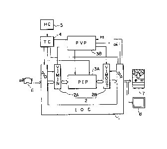
An example of the video image processing
system of Fig. 1 aims at a higher-speed data processing
and comprises an input/output section 1 (IOC), a memory
section 2 (VIM) including an input image memory 2A
(VIMINJ and an output image memory 2B (VIMOUT), a data
processing section 3 including a position invariant
processor 3A (PIP) for mainly calculating a pixel value
and a position variant processor 3B (PVP) for
accomplishing data flow control such as the address
control and for effecting the timing control, and a
processor 4 (TC) as a controller of the overall system
for controlling the execution of processing, termination
of processing, and program exchange. To the TC 4, a
host computer 5 (~P) is connected to control the overall
video image processing system.
~L2~3~18
The IOC 1 is configured such that, for
example, a video signal from a video camera 6 or a VTR
is subjected to an A/D converslon to obtain a digital
image data, which is then written in the VIMIN 2A;
furthermore, a processed image data is read from the
VIMOUT 2B and is restored into an analog video signal
through a D/A conversion, which is then recorded, or
example, in a VTR 7 or is supplied to a monitor image
receiver 8, thereby enabling a video image to be
monitored.
In addition, other than the digital data,
signals for externally controlling the VIM 2 such as a
clock, a dominant mode signal, an address, and a write
control signal are supplied from the IOC 1.
In this case, the signals which can be
inputted to or outputted from the IOC 1 are signals of
the NTSC system or the R/G/B system. The signal system
is specified through the TC 4. Moreover, a pixel is a
data item comprising eight bits, for example.
A read or write operation of the VIM 2 is
achieved in a group of an image, namely, a field or
frame unit. To this end, the VIMIN 2A and VIMOUT 2B
each include a plurality of memory sheets each having a
capacity of a field or frame of image data. For
example, 12 sheets of 768 x 512 byte frame memory are
provided. In this case, the utilizatioll of these 12
sheets of frame memory is not fixed, namely, the 12
- sheets can be arbitrarily allocated as the VIMIN 2A or
the VIMOUT 2B according to the processing purpose or the
;I processing objective image. Moreover t the memory sheets
are designed t-o be used in a pair and when a sheet of a
pair is in the write state, the other sheet can be used
for a read operation, which enables the IOC 1 to achieve
parallel processing of an external processing through
the VIM 2 and the internal processing through the VIM 2
by use of the PIP 3A and the PVP 3B.
In this case, the dominant mode signal to
determine whether the sheets of frame memory of the VIM
2 are under control of the IOC 1 or the PVP 3B is
generated from the IOC 1 and is supplied to the VIM 2.
Moreover, the address of digital data to be
processed, the write control signal, the read mode
signal, and data select signal for internally
controlling the VIM 2 are supplied from the PVP 3B to
the VIM 2, and then the data stored at the address is
transferred to the PIP 3A for the processing thereof.
Furthermore, the data processed in the PIP 3A
is supplied to the VIM system 2, and then an address and
.
-- 9
lZ~3~3~8
other information are supplied from the PVP 3B to the
VIM 2. As a result, the digital data thus processed is
written in the VOM 2.
Moreover, an address and other information are
also supplied from the VIM 2 ~o the IOC 1, which causes
~I the digital data read as a result to be supplied to the
IOC 1, and then the digital data is converted into a ..
predetermined analog video signal through a DA - -
conversion and other processing so as to be fed to an
output terminal.
The data processing section 3 has a processor
and reads the image data stored in the VIMIN 2A
according to a program of the processor and executes
various kinds of data work processing thereon, and then
the processed data is written in the output image memory
2B.
The data processing section 3 is subdivided
into the PIP 3A and the PVP 3B; consequently, as
compared with the conventional data processing section
requiring tbe processing time equal to the total of the
processing time of these subsections, the data
processing section 3 requires only the larger processing
time thereof because of provisions of these subsections.
Consequently, the case of this example realizes a high-
- 10 -
:~2~3~1~
speed processing which almost allows the video data
processing to be executed through a realtime processing.
The processor of the data processing section 3
includes one sheet of processor or several sheets of
processors, and the microprogram contained in the
microprogram memory thereof can be changed if it is
required to expand the processing capability.
The microprogram is temporarily supplied from
the HC S to the TC 4 so as to be stored in an RAM
disposed therein; and thereafter, for example, in
response to a program change request from the user (by
setting the pertinent switch to ON), the microprogram is
supplied from the TC 4 to each processor, thereby
changing the ~icroprogram.
~; The-PIP 3A and the PVP 3B each are of the same
arch1tecture and are independent processors each
~; including a control section, an arithmetic section, a
memory section, and an input/output port. These systems
are respectively structured in a multiprocessor
configuration comprising a plurality of unit processors
in which a high-speed processing is mainly implemented
according to the parallel processing scheme.
The PIP 3A has, for example, 60 sheets of PIP
processors and several sheets of subprocessors, so that
,
3~
the working of the image data from the VIM 2 is
accomplished or the image data is generated in the PIP
3A.
The PVP 3~ includes, for ex~mple, 30 sheets of
processors to control the flow of the internal i~age
data with respec~ to the VIM 2, for example, to effect
allocation and recovery of the image data obtained from
~; the VIM 2 on the PIP 3A.
That is, the PVP 3B generates an address data
I and a control signal to the VIM 2 and supplies them to
the VIM 2; and the PVP 3B generates the input/output
control signal of the PIP 3A and other control signals
and supplies them to the PIP 3A.
As for the image data processing, there is not
only the cas~ where the data from a frame of the input
image memory 2A is processed and the processed data is
i written in the output image memory 2B but also a case
where the data stored in a plurality of frames from a
plurality sheets of frame memory is processed.
In addition, the number of bits to be
~: processed in the PIP 3A and the PVP 3B is 16 in the
standard specification, and for the arithmetic
processing of the image data processing, it is enabled
to implement a processing speed at which the processing
- 12 -
P3~
can be implemented within a frame, namely, the realtime
processing can be achieved for the l-frame image data.
There exist naturally a processing which requires a
processing time exceeding a frame.
In this case, the image data processing of the
PIP 3A and the PVP 3B is accomplished in synchrony with
the frame. Consequently, the PVP 3B is supplied from
the IOC 1 with a processing start timing signal PS
synchronized with the frame. The PS signal is normally
at a high level and is set to a low level when the
processing start timing is detected. On the other hand,
the PVP 3B supplies the IOC 1 with a signal OK
indicating that a processing has been completed. This
signal OK is outputted from the primary processor among
the processors of the PVP 3B when the processing is
completed, the processor controlling the timing of the
processing system.
That is, in a step 101 of the program
flowchart of Fig. 2 as an example of means to output a
signal OK from the processor, the primary processor of
the PVP 3B softwarewise detects a fact that the
processing start timing signal PS from the IOC 1 is set
to the low level. When the condition that the signal PS
is set to the low level is detected, the processor
- 13 -
.~ .
~2~3~1~
starts its operation and outputs a timing signal TS by
use of a pr~gram to the other processors including the
PIP 3A, and then supplies an address to the VIM 2, reads
an image data from the VIM 2, and performs a work
processing in the PIP 3A (step 102). When the
processing is finished, the signal OK is outputted and
the processing is terminated (step 103) to wait for the
next processing start timing signal PS tstep 1~1).
The signal PS is generated by the IOC 1 as
follows.
The IOC 1 is configured as shown in Fig. 3,
for example.
That is, the PLL circuit 11 for generating a
clock generates the clock wh~ch is locked for the phase
of, for example, the subcarrier of the input video
signal.
The interface 12 effects a division on the
clock from the PLL circuit 11 and applies a delay on
some of the resultant signals, and then the obtained
signals are transmitted to the relevant sections in the
IOC 1, the VIMIN 2A, and VIMOUT 2B.
: In the A/D converter 13, the input video
signal is converted by use of a sampling clock ~for
exampler 14.32 MHz) from the interface 12 into the
- 14 -
.
" ' ,
.
.
3~318
digital image data in which eight bits are generated for
each sampling.
The input circuit 14 is supplied with a
digital image data from ~he A/D converter 13, and the
data is transferred to the VIMIN 2A to be written
therein.
In this case, a signal specifying the signal
system (NTSC or R/CjB system) is supplied from the TC 4
to the input circuit 14. For the NT5C signal, two
sheets of frame memory ~or exceeding two sheets) are
assigned as ~he input image memory and the data is
alternately written in the memory. On the other hand,
for the ~/G/B signal, six sheets of frame memory among
the 12 sheets thereof are assigned as the input image
memory and the data is alternately written in two sheets
of frame memory for each principle color. The data is
read from any frame memory for which the write operation
is not conducted.
As described above, the image data stored in
the memory is separated from the IOC 1 and the data flow
is then controlled by the PVP 3B.
In this case, this input circuit 14 supplies
the VIMIN 2 with only the effective signal of the image
signal from which the~sync signal and the burst signal
-- 15 --
93~
portion are removed and the obtained signal is written
in the frame units according to the clock delivered from
the interface 12.
In addition, in the input circuit 14, the
phase of the burs~ signal in the video signal and the
phase of the ciock are compared, and the output of the
comparison result is supplied as a phase c~ntrol signal
to the PLL circuit 11. The clock from the PLL 11 is-
subjected to the phase lock operation with respect to
the subcarrier in the video signal.
Moreover, in the input circuit 14, a signal
for extracting the burst signal, a valid/invalid signal
indicating whether or not the sync signal and the burst
signal portion are included in the image signal, a frame
start signal FL indicating the first line of each frame,
a signal indicating the vertical blanking of each field,
and a video ID signal with a signal indicating the start
of the line are generated and are used therein;
furthermore, these signals are supplied for the
processing thereof to the output circuit 15 to be
described later.
The output circuit 15 is supplied with the
process~d video data r~ad from the VIMOUT 2B on the
frame-by-frame basis.
lZ93818
In the data thus read, the sync signal does
not include the burst signal; consequently, the out?ut
circuit 15 includes an ROM for generating a sync signal,
a burst signal, and a vertical blanking ;ignal. In the
NTSC signal system, the data from the VIMOUT 2B is sent
to the D/A converter together with the sync signal, the
burst siynal, and the vertical blanking signal (after - -
being rearranged if necessary)O
In addition, in a case of the signals
representing three principle colors, an external sync
signal is also required, and the sync signal is also
regenerated by this output circuit 15 and is supplied to
circuits such as for the monitor.
Furthermore, the output circuit 15 generates a
signal for controlling the VIM 2. Namely, a dominant
mode signal for indicating whether the VIM 2 is in the
mode to be controlled by the IOC 1 or by the PVP 3B is
generated and is fed to the VIM 2. Among the frame
memory sheets of the VIM 2, only a memory to which an
input data is delivered or from which an output data is
read according to the dominant mode signal is placed
under control of the IOC 1. The change-over timing of
the domlnant mode signaI is determined according to the
signal OK.
' .
- 17 -
.
'
~3~318
The output circuit 15 further generates an
address signal of the VIM 2 and a write enable signal
for controlling a read/write operation, and the signals
are transmitted to the memory under control of the IOC 1
associated with the VIM 2. The memory dominated by the
PVP 3A i.s supplied wlth the address and other control
signals fro~ the PVP 3B.
Moreover, the output circuit 15 generates a
processing start timing signal PS from the frame start
signal FL indicating the first line of each frame from
the input circuit 14 and the processing end signal OK
from the PVP 3B.
That is, in an example of means for generating
the signal PS as shown in Fig. 4, the frame start signal
FL is at a qow level for a period of a clock at the
start point of each frame (Fig. SA). The frame start
signal FL is delayed by a period of a clock in the delay
` circuit 17 and is then supplied to the clear terminal of
the D-type flip-flop 18. On the other hand, at the end
of the processing, the clock terminal of the flip-flop
18 is supplied with a signal OK from the PVP 3B to be
set to a high level for a period of a clock 8 Fig. 5B).
Moreover, the D input of the flip~flop 18 is
always at the high level.
: - 18 -
~ ?~
Consequently, until the signal OK is received,
this flip-flop 18 is cleared by the frame start signal
FL and hence the Q output DP thereof (Fig. 5C) is kept
remained at the high level.
When the signal OK is received, the output DF
of this flip-flop 18 is set to the low level.
The output DF is supplied to the OR gate 19.
The OR gate 19 is in turn supplied with a frame start
signal FL. ~he output from this OR gate 19 is the
signal PS (Fig. 5D), and if the frame start signal FL is
received when the output DF is at the low level, the
output PS i5 set to the low level for a period in which
the signal FL is at the low level.
Only when the signal OK is obtained, the
rocessing start timing signal PS synchronized with the
frame can be attained.
When executing a realtime processing, the
signal OK is obtained for each frame end in any case,
and hence the signal PS becomes identical with the frame
start signal FL.
On the other hand, if the processing time is
longer than a frame, the signal PS is different from the
frame period and can be first obtained only in the next
frame following an output of the signal OK.
-- 19 --
. - ... ; .. , ,.. . .. -
~2~3E~
In the case of this example, the following
three modes can be selected for the image data
processing.
1 A processing is conducted once per N frames.
The realtime processing is executed for N = 1.
2 The frame subsequent to the point of time when
the preceding processing is finished is automatically
fetched for the processing.
3 The frame following the time of point
indicated by the user, for example, through a push
button, is fetched for the processing.
Although, in the case described above, the
entire data processing is automatically accomplished
without necessitating the human intervention, namely,
the frame next to the time of point when the preceding
processing is finished is automatically fetched for the
processing, it is also possible that to enable the user
to process the desired frame data, a manual switch is
disposed for this purpose; and when the user specifies a
frame to be processed, the signal PS is to be gated at
the specified frame, that ic, the slgnal PS is obtained
only at the start point of the specified frame.
In this invention, since the processing start
timing signal is generated after a signal indicating the
- 20 -
1;293~8
completion of a data processing is received from the
data processing section, there does not occur an
nconsistency that the next processing start signal is
generated before the preceding processing is finished.
Moreover, the processing start timing need not
be determined with a maryin of rocessing time, and hence
an effective data processing can be accomplished.
The image data processing is effcted as
described above.
In the data processing section 3, an image
processor achleving the computer processing is used. In
this case, by use of the characteristic o the image
data which is regularly arranged in a 2-dimensional
array, a method for arranging a plurality of unit
processors each having the same configuration and for
simultaneously operating the processors at the same time
is adopted as a method for processing the image data at
a high speed.
In a system in which a plurality of subsystems
coordinate with each other to execute a processing, it
is necessary to correctly control the operation timing
for indicating the processing start and processing
branch of each processor.
'
- 21 -
:;
~2931~8
In this case, in addition to a case where the
plurality of processors can be controlled at the
completely sa~e operation timing, there are cases where
the different timing is required, namelyt each processor
must be started with a slight timing difference. as a
method for controlling the timing, it is common to
effect an independent timing control by independently
sending a operation timing signal to each subsystem
rather than to effect the timing control with a timing
control system.
However, in a case where each subsystem is
independently controlled, the equal number of timing
control lines and subsystems are required, which leads
to a difficulty that the size of the timing control
system 100 becomes large.
To overcome this difficulty according to the
present invention, as shown in fig. 6, the timing signal
is shared among the plurality of subsystems.
In the configuration of Fig. 4 showing the
timing control section, a timing control processor 30 is
disposed as the maln processor in the PVP 3B as
described before. The processor 30 is supplied with the
processing start signal PS from the IOC 1. The IOC 1 is
in turn supplied with the processing end signal OK from
the processor 30.
- 22 -
~293~318
When a condition that the processing start
timing signal PS is set to the low level is detected,
the processor 30 sends as a tlming signal TS a time
series signal having a width of one bit to the other
processors 31, 32, 33, etc. in the PVP 3B; furthermore,
the timing signal TS is transmitted also to the
processors 34, 35, 36j etc. of -the PIP 3A. In this
case, the 60 sheets of processors in the PIP 3A are
controlled in groups each including ten sheets of
processors.
The processors 31, 32, 33, etc. and 34, 35,
36, etc. each are provided with a decoder for the timing
signal TS.
:~ In an example of the decoder shown in Fig. 7,
the decoder comprises a shift register 37, a bit pattern
setting unit 38, and a comparator 39.
The shift register 37 sequentially receives
the timing signal TS from the control processor 30. In
this case, the shift clock of the shift register 37 is
synchronized with the transmission timing clock of the
: timing signal TS or is a clock having a frequency higher
than the frequency of the transmission timing clock.
The timing signal TS is transmitted in the
bit-by-bit basis in response to the transmission timing
- 23 -
.
~;~93~
clock, so that the signal i5 fetched into the shift
register 37 such that, for example, a bit pattern of
five bits are sequentially shifted bit by bit.
A particular bit pattern specific to each
processor is set to the pertinent bit pattern setting
unit 38.
The comparator 39 compares the 5-bit pattern
of the timing signai TS stored in the shift register 37-
with the 5-bit pattern in the setting unit 38. If the
patterns match with each other, the operating timing
signal TP of the processor to which this decoder i5 set
is delivered from the comparator 39.
¦ Assuming now that, for example, a bit patter
~1001] is contained in the setting unit 38, the
comparator generates an operation timing signal TP at
: the timing when the bit pattern of the shift register 37
changing for each transmission clock becomes to be
[1001] .
Consequently, if a bit pattern to be set to
the bit pattern setting unit 38 of each decoder of the
processors 31, 32, 33~ etc. and 34, 35, 36, etc. is
assigned for each processor, the operation timing signal
~P is respectively generated at the specific timing.
- 24 -
~L25~3~i8
In this case, the timing control processor 30
saves the bit pattrn of ~he setting unit 38 of each
decoder of the processors and performs and arithmetic
processing, for example, to determine the transmission
sequence of [0111] of the timing signal TS so as to
supply a desired operation timing to each processor, and
then the timing signal TS is sent to the processo~s,
thereby accomplishing the timing control of each
processor.
In this case, the bit pattern to be set by the
bit pattern setting unit 38 may contain data of which
the number of bits is equal to or more than the number
of bits of the shift register 37; furthermore, the
number of bits may vary for each register.
For example, in a case where the processing is
to be started when ~101] and [1001] are detected for the
processors 31 and 34, respectively, if a time series
signal [1] ... [11011] ... ~100111 ... is transmitted as
the timing signal, the processors 30 and 34 càn be
operated at the preceding timing of ~101} and at the
succeeding timing of rlOOl], respectively.
In addition, in a case where the processing is
to be started when ~10l and ~100] are detected for the
processors 32 and 33, respectively, if a time series
~`
- 25 -
.
31318
signal 11] ... Elloll] ... is transmitted as the timing
signal, the processors 33 can be operated at the
preceding timing delayed by a transmission clock cycle
with respect to the processor 32.
Incidentally, without disposing the decoder as
shown in Fig. 5, each processor can perform a software
processing to detect the bit pattern, thereby obtaining
the operation timing.
Moreover, other than the bit pattern described
above, [1] may be transmitted in other than the
transmission of the timing signal TS and [O] may be sent
in the transmission of the timing signal TS, so that
each processor counts the frequency of [1] to determine
the operation timing. In this case, the frequency may
be changed ~or each processor so as to determine the
specific operation timing for each processor.
As described above, the timing signal TS may
be other than one bit wide, namely, the width may be of
several bits; however, in such a case, the bit-parallel
signal comprising a plurality of bits is required to be
used as the timing signal, and hence a plurality of
transmission lines are required. In a case of a l-bit
wide signal, only a transmission }ine is required.
- 25 -
,~,. . ... . .
3L293~
As described above, according to the present
invention, the timing signal is shared among a plurality
oi subsystems and the decode processing of the timing
signal in each subsystem, namely, the algorithm for
detecting the operation timing of each subsystem i5
changed, thereby enabling to supply the respective
processing timing to the plurality of subsys~ems by use
of a small-sized hardware.
The processors constituting the PIP 3A and the
PVP 3B each comprises a control section provided with a
microprogram stored therein for outputting a
microinstruction and an arithmetic section for executing
an arithmetic operation according to the
microinstruction. The input digital data is supplied to
the arithmetic section. A portion of the information of
the arithmetic section is fed to the control section so
as to reflect the arithmetic inormation to the program
and the result of the arithmetic operation is obtained
as an output digital data from the arithmetic section.
The arithmetic section o the processor
includes a multiplier, an adder/subtractor, and a factor
memory for storing factors or coefficients necessary for
the arithmetic operation such as for sing B and cos ~.
- ~7 -
313~
In the processor described above, in addition
to the signal value calculation for calculating an
output data value from the input data, t:here are various
kinds of values associated with other than the signal
value calculation, for example, an address for
determining a factor to be read from the factor memory
and a count of a so-called DO loop to be determined
according to the processing content.
However, in a case where the calculation of
the various knds of values other than those related to
the signal value calculation is also accomplished by use
of the arithmetic section achieving the signal value
calculation, the calculation time therefor is
particularly required, which lowers the data processing
speed.
Fig. 8 is a block diagram showing the overall
configuration of an example of a processor for the
digital operation to be used in the data processor
according to the present invention. In this example,
the microinstruction from the control section 100 is
supplied to the main arithmetic section 300 and the
auxiliary arithmetic section 200.
The main arithmetic section 300 is supplied
with an input data, which is then subjected to a signal
- - 28 -
~3~318
value calculation, and then an output data is generated
and is delivered.
The auxiliary arithmetic section 200 generates
addresses of the factor memory and the data memory
disposed in the main arithmetic section 300 as will be
described later and performs a computation for obtaining
the value of repetition of the DO loop, and the
addresses and the DO loop repetition value are delivered
to the main arithmetic section 300 and the control
section 100, respectively.
Fig. 9 is A block diagram showing an example
of the main arithmetic section 300 in which two systems
of data operation units each for 8-bi~ operation are
provide for the general-purpose processing, so that a
16-bit data operation is enabled in the system as a
whole.
That is, the arithmetic units 300X and 300Y
each have the completely same configuration, and hence
the same reference numerals are assigned to the .
corresponding sections thereof together with suffix
: letters X and Y.
: Namely, the first arithmetic unit 300X
comprises a multiplier 311X, an adder/subtractor 312X, a
factor memory 313X, a data memory 314X, a plurality of
29 -
1293~
registers 321X - 328X, and a tristate buffers 331X -
338X.
The control section 100 sends
microinstructions to determine whether or not the
outputs from the registers 321X - 328X are to be
enabled, whether or not the data is to be fetched, or
whether or not the multiplier 311 is to be operated.
The tristate buffers 331X - 338X are also
controlled by the microinstructions.
In the first arithmetic unit 301X, the input
data is fed to the register 321X and the registér 328X
delivers an output data.
The factor memory 313X contains the factor or
coefficient data such as cos B and sin ~. When an
address signal is supplied from the auxiliary arithmetic
section 200 via the register 341XY to the factor ~emory
313X, a factor necessary for a signal value calculation
is appropriately read therefrom.
The data memory 314X is used to store the
output data generated when necessary. when an address
signal is supplied from the auxiliary arithmetic section
200 via the register 342XY to the data memory 314X, the
data is read therefrom as appropriately.
- 30 -
1~931~
The second arithmetic unit 300Y is similarly
configured in which the input data is supplied to the
register 321Y and the register 328Y delivers an output
data. An address from the auxiliary arithmetic section
200 1s supplied via the register 341XY to the factor
memory 313Y, whereas an address from the auxiliary
arithmetic section 200 is fed via the register ~42XY to
the data me~ory 314Y.
In this case, the first arithmetic unit 300X
and the second arithmetic unit 301Y are so designed to
process 16-bit data, namely, 32-bit data can be
processed in the system as a whole. ~he system is
configured to be capable of achieving a general-purpose
processing so that the processing may be effected on
either one of the ~irst and second arithmetic units 300X
and 300Y; moreover, ~he outputs from the
adder/subtractor 312X and 312Y are supplied to the
registers 323Y and 323X, respectively, whereas the
outputs from the registers 327X and 327Y are delivered
to the register 324 and the multiplier 311 and the
register 324X and the multiplier 311X, respectively,
thereby enabling information communication between the
arithmetic sections 300X and 300Y.
- 31 -
~2~3~
Furthermore, the adder/subt~ac~or units 312X
and 312Y are linked to each other by use of a joining
section 350. When a predetermined select signal lS
supplied to the joining section 350, the operation can
be changed between two modes, namely, whether the
respective adder/subtractor units 312X and 312Y each
operate as a 16-bit adder/subtractor with the single
precision or two adder/subtractor units 312X and 312Y
operates as a unit to operate as a 32-bit
adder/subtractor witb the double precision.
In this example, the adder/subtractor units
312X and 312Y each are constituted as a 16-bit
adder/subtractor, for example, including four
microprocessors Am2901 of A~D as a unit. The
adder/subtractor, for example, includes a RAM which is
capable of storing 16 items of 16-bit data. The 16-bit
data items are arranged so as to be shifted in the
column direction according to the numeric relationships
such as 1/2 time, 2 times, and so on.
In a parallel processing system based on the
above-mentioned multiprocessor configuration, the TC 4
performs a comprehensive control in three modes to be
described later, thereby enabling the processing
execution, the processing termination, and the program
transfer ~exchange) without any inconsistency.
- 32 -
1;Z93~
Fig. 10 shows the connecting relationships
between the TC and the control section 100 of one of the
plural processo-s of the PIP 3A and the PVP 3B~ This
confi~uration applies to all the processors effecting
the program exchange.
That is, in this diagram, the components other
than the TC 4 constitute an example of the configuration
of the control section of the processor.
The microprogram controller 101 generates
addresses of the microprogram memory 111 - 114a and 114b
constituted ~rom the RAM.
From the microprogram memory 111, for example,
four instruction bits are obtained to select one of a
plurality of instructions of the microprogram controller
110, and the instruction bits are supplled via a
register 115 to an instruction terminal I of the
controller 110.
In this case, the controller posseses 16 kinds
of instructions.
Moreover, the selector 116 is supplied with a
plurality of l-bit information items, and one of these
items is selected according to an information read from
the micropro~ram memory 112. The l-bit information from
the selector 116 is supplied as a condition code to the
- 33 -
.~
. .
lZ93~
terminal CC of the program controller 110 and is then
combined with the instruction bits so as to be used as
an information to select the next address as a data
incremented, an address to be supplied to the direct
input terminal D, or other address.
; An information, for example, a destination
address of a GO TO statement or an information of the
repetition value of a DO loop is ob~ained from the
microprogram memory 113 and is then latched into a
register 117a.
Form the micro program memory 114a and 114b,
an information of the microinstruction is extracted.
this information is supplied via the register 118 to the
arithmetic section of this processor, and all or a part
of the microinstruction is supplied to the add/subtract
logic unit 201 as an auxiliary arithmetic section 200.
The micropro~ram controller 110 is so designed
to enable one of three enable signals PL, VECT, and MAP
depending on the instruction bit. Consequently, one of
the registers 117a - 117c is enabled by the instruction
bit, and the address latched in the register is used as
the direct input. In most instruction, the signal PL is
enabled, namely, the signal VECT or MAP is enabled only
for a particular instruction. Furthermore, whether the
- 34 -
~29~
direct input is ~o be selected in the instruction bit
state is determined according to the conclition code from
the selector 116.
On receiving a microinstruction, the
add/subtract arithmetic unit 201 obtains through
calculation address signals of the factor memory 313X
and 313Y and the data memory 314X and 314Y of the main
arithmetic section 300 and supplies the obtained address
signals to the registers 341XY and 342XY for the
storage.
In the add/subtract arithmetic unit 201, an
information such as the repetition value of a DO loop is
obtained through a computation and is fed, for example,
to the register 117b for the storage.
: Operations in the auxiliary arithmetic section
200 are relatively simpler than the signal value
calculation of the main arithmetic section 300;
consequently, as the example described above, the
auxiliary arithmetic section 200 can be of a small size
as hardware like the add/subtract arithmetic unit 201.
As described above, when the auxiliary
arithmetic unit 200 is provided, for example, in a case
where a computation of the total of operations between
the coefficients KA(al), KA(a2), ... RA(an) at the
- 35 -
~3~18
addresses al, a2, ... an of the factor memory 313X and
the data TA(al), TA(a2), Ø TA(an) at the respective
addresses of al, a2, -- an of the data memory 314X,
namely,
KA (al) * TA (al) + KA (a2) * TA (a2) + + RA (an) *
TA(an) and a computation of the total of operations
between the coefficients KB(al~, KB(a2), -- KB(an) at
the addresses.al, a2, -- an of the factor memory 313Y . .
and the data TB(al), TB(a2), -- TB(an) at the
respective addresses of al, a2, -- an Of the data
memory, namely,
KB(al) * TB(al) + KB(a2) * TB(a2) ~ KB(an) *
TB(an) are effected at the same timè, the processing can
be accomplished in n steps or slightly greater than n
steps as compared with 2n steps required in the prior
art technique, which enables to improve the processing
speed.
According to the present invention, since the
auxiliary arithmetic section is provided to calculate
values such as the memory address of the factor memory
of the main arithmetic section performing the signal
value calculation, the operations such as the a~dress
value calculation conventionally achieved in the main
arithmetic section are reli~ved therefrom, and hence the
- 36 -
.,
lZ~315 ~8
main arithmetic section effects only the signal value
calculation~ thereby increasing the execution speed of
the processing.
Furthermore, since the operations in the
auxiliary arithmetic section do not necessitate a large-
sized hardware in most cases required by the signal
value calculation in the main arithmetic section, which
leads to an advantage that only a small-sized hardware
is added ton the auxiliary arithmetic section.
In a case where a so-called adaptive
processing is executed according to the information from
the arithmetic section and other processors, the
selector 116 is supplied as an input information the
information from the arithmetic section and the
information from other processor, and depending on the
information, an instruction, for example, a conditional
jump is effected.
However, in a case of the programming system
for the adaptive processing described above, even a
trifle adaptive processing, for example, a calculation
of an absolute value gives an influence on the flow of
program addresses due to a conditional jump or the like.
Moreover, when several data flows exist for
the respective arithmetic processing in a processor,
- 37 -
'
''
...
lZ~
there arises an inconvenience that a program generated
by use of such a condition code cannot cope with the
processing of the data associated with the respective
data flows.
In the present example, the memory units 1i4a
and 114b are provided as the microprogram memory for
supplying microinstructions to the first data system.
The outputs from the memory 114a and 114b are connected
~wired ORed) with each other and are linked via the
register 118 to the first data system.
The information from the first data system is
supplied as the chip select signal CSl to the memory
114a and is delivered via an inverter 122 to the memory
114b.
A~ an example, the contents of the
microprogram memory 114a and 114b in a case where a
computation of C = A + IB¦ is achieved will be as
follows.
Address Contents of memory Contents of memory
114a 114b
. _
Input data A to ALU Input data A to ALU
1 Check the sign of B Check the sign of B.
. _ _ __
2 C = A t B C = A - B
__ _. _
:
- 38 -
~93t3~8
That is, although the contents of the
addresses O and 1 of the memory 114a and 114b are the
same, the contents of address 2 varies depending on the
sign of data B. Since the signal of the digital data is
positive if the MSB is O and the signal is negative if
the MSB is 1, the MSB of the data B is supplied as the
chip select signal CSl. As a result, if the MSB is-O
indicating the positive sign, the memory 114a is
selected and an operation C = A + B is accomplished in
the arithmetic section, whereas if the MSB is 1
indicating the negative sign, the memory 114b is
selected and an operation C = A - B is executed in the
arithmetic section.
As described aove, without changing the
address flow, namely, the program flow itself, an
adaptive processing such as a calculation of an absolute
value can be conducted.
That is, with the provision that based on a
signal of a data system, a program memory associated
with instructions controlling the data system can be
selected, the adaptive processing can be easily
accomplished for each data system.
If the address capacity of the program memory
is greater than the program length, it is possible to
- 39 -
~2~3~3~L8
dispose two memory such as the memory 114a and 114b of
the example described above. These memory units are not
selected through a chip select opera~ionl namely, two
kinds of program contents are writ~en in a memory
device, thereby enabling to select one of these two
kinds of programs by supplying the informa,ion from the
data system to the MSB of the address.
According to ~he present invention, since a
p~urality oE program contents are prepared and one of
the programs is selected depending on the information
from the data system, the adaptive processing associated
with the information from the data system can be simply
achieved without changing the program flow.
Moreover, when the ~-bit instruction from the
register 115 is ~0000], a [JUMP ZERO] instruction is
assumed and the microprogram controller 110 is set to a
state to output an address 0 in any case regardless of
the condition code.
On the other hand, the TC 4 comprises an RAM
41 for storing programs to be supplied to the
microprogram memory 111 - 114a and 114b and an address
generator 42 for generating the addresses thereof.
In addition, to implement three modes
including the execution mode, the reset (halt) mode, and
- 40 -
the program exhange mode, the mode sig.nal generate means
43 is disposed to generate l-bit mode signals MA and MB;
furthermore, there is providea ~he write signal generate
means 44 for generating a program write signal for the
microprogram- memory lll - 114a and 114b in the program
exchange mode.
The mode signal generate means 43 is
configured, for example, as shown in Fig. 11. . .-
That is, switches SWA and SWB are to be
changed over by the operator. ~ach switch has an input
A applied with a positive direct current (dc) voltage
and other terminal B grounded. A signal a to be
obtained by the switch SWA is supplied to an input
terminal of an OR gate 45. A signal b obtained by the
switch SWB is delivered as a mode signal MB and is
supplied to other input terminal of the OR gate 45,
which in turn delivers a mode signal MA.
In this case, the mode is set as follows
depending on the l-bit mode slgnals u~ ~nd UB.
- 41 -
.;
.. ... ,., ,.. ,.. ,. .. , . . ,.. ;. . .:.: .
.
.
.~A = O MB = O I Program exchange mode
. ~
~ MA = 1 MB = O Reset (halt) mode
. _
MA = 1 MB - 1 Execution mode
Table 1
; That is, when the switch SWB is set to the
terminal A, the execution mode is set regardless of the
state of the switch SWA. If the switch SWA is set to
thefterminal A and the switch SWB is set to the terminal
B, the reset mode is set. If the switch SWB is set to
the terminal B and the switch SWA is set to the terminal
B, the program exchange mode is set.
As can be seen from Table 1 listed above, when
the signal MB is 0, the program execution is stopped,
and when the signal MB is 1, the program becomes
executable. Consequently, this mode signal MB is
signified as a reset (halt) signal.
On the other hand, when the signal MA is 0,
the program exchange is possible. This mode signal MA
is therefore signified as a change signal.
These two mode signals MA and MB are used to
establish the respective modes as follows.
- 42 -
. . ;, . , ... -
1~3~
That is, the selector 120 selects addresses
for the microprogram memory 111 - 114a and 114b from the
addresses ~rom the program controller llO and the TC 4.
As a select signal for this purpose, the signal MA is
supplied. When the signal MA is l, the address from the
microprogram controller llO is selected, and when this
MA is 0, the address.from the TC 4 is selected.
In addition, the gate cir'cuit 121 gates the
write signal WR according to the gate signal MA. When
the gate signal MA is 0, the gate is opened and the
signal WR is supplied to each write enable terminal WE
of the microprogram memory lll - 114a and 114b.
When 0 is supplied to the WE si,gnal of the
microprogram memory lll - 114a and 114b, the
microprogram memory are set to the write enable state.
Moreover, the signal MB is fed to the reset
terminal of the register 115, and when this signal MB is
0, the register 115 is reset.
In the TC 4, the states of the mode signals MA
and MB are monitored by the load control section 46 so
as to control the processing in the TC 4 accordi,ng to
the modeO
In the program execution mode, the mode signal
~A is l, and hence an address from the microprogram
- 43 -
.
. . .~. .
.. .... .
..
,
93~3~8
controller 110 is obtained from the selector 120, and
this address signal is subjected to a delay of a clock
via the register 119 and ~he resultant si~nal is
supplied to the microprogram memory 111 - 114a and 114b.
Furthermore, the outp~t from the OR gate 121
is 1 in any case when the signal ~A is 1/ and the memory
111 - 114a and 114b are therefore not set to the write
enable state.
In addition, since the mode signal MB is 1,
the register 115 is not reset and the data read from the
microprogram memory 111 is subjected to a delay of a
clock in the register 115 and is supplied to the
instruction terminal of the microprogram controller 110,
thereby executing a program.
InIthis case, the microinstruction read from
the microprogram memory 114 is delayed by a clock in the
register 118 and is supplied to the arithmetic section.
In the execution mode, the pipeline registers
are designed to be disposed as follows. A register 119
is located between the program controller 110 and the
microprogram ~emory 111 - 114a and 114b, the registers
115 and 117a are disposed between the output sides of
the microprogram memory 111 - 114a and 114b and the
program controller 110, and a register (not shown) is
- 44 -
~33~
connected to the input of the selector 116~ This
provision enables to decrease the clock cycle.
That is, in the image processing system of
this example, the parallel processing method by use of
the multiprocessor configuration is primarily adopted,
however, the pipeline processing method as described
above is also partly utilized to effect a high-speed
processing.
In the program transfer mode, the mode signal
MB is 0, and hence the register 115 is reset and ~0000]
is supplied to ~he instruction terminal of the program
controller 110; consequently, the address supplied from
this program controller 110 is kept to be 0 or the
address output is stopped. Namely, the program
addresses for all processors associated with the PIP 3A
and PVP 3B are 0 and hence the program stop state is
set.
On the other hand, since the mode signal MA is
also 0, the selector 120 is set to the state to select
the address from the address generator 42 of the TC 4.
That is, in the program transfer mode, the
microprogram memory of all processors is under control
of the TC 4.
-
- 45 -
. : .
, .
~29315 ~L~
In this case, moreover, the signal MA may be
fed to the output enable terminal OE of the program
controller 110 so as to set the output buffer of the
program controller 110 to off.
Furthermore, according to the program
undergone the program transfer executed by the TC 4 in
the program transfer mode, an instruction from the.load
control section 46 causes the address generator 42 to
send an address to the RAM 41, and the program data to
be transmitted to the microprogram memory 111 - 114a and
114b.is read from the .RAM 41. At the same time, the
write signal WR.from the write signal generate means 44
is set to 0 and the mode signal MA is 0; consequently,
the output from the OR gate 1~1 is also set to 0, which
sets the microprogram memory 111 - 114a and 114b to the
write enable state.
As a consequence, the program data from the
RAM 41 is sequentially written in the microprogram
memory 111 114a and 114b according to the address from
the address generate means 42, thereby achieving the
program transfer.
In this example, the program transfer is
sequentially accomplished for each processor.
- 46 -
1293~3i8
That is~ the TC 4 is provided with the ROM 47
in which the processor select signal is stored. ~hen a
program is transferre~ from the ROM 47, the processor
select signal is read according to an instruction from
the load control section 46. The processor select
signal is decoded in the decoder 48 and only the select
signal SEL for the processor to be selected is set to 0
and the other signals are set to 1. The select signal
SEL is kept supplied to the OR gate 121, and only the
microprogram memory 111 - 114a and 114b of the processor
for which the select signal SEL is 0 is set to the write
enable state, and then a program rewrite operation is
effected.
When a write operation is completed in a
microprogram memory of a processor, the a processor
signal for another processor is extracted from the ROM
47 and the select signal SEL of the processor is set to
0; similarly, the program transfer to this processor is
achieved~ To change the programs of all processors, the
operation described above is repeated as many times as
there are the processors.
In this case, if a plurality of programs are
to be sent to each processor or if a plurality of
different programs are to be~transmi~ted to each
- 47 -
. :.
3~
processor, these programs are written as a unit in each
processor. In each processor, the program to be next
executed is specified by supplying an execution start
address to each processor.
The execution start address is extracted from
the RAM 49 and is supplied to the register 117c of each
processor. The select signal SEL is delivered as a
latch signal of the register 117c, and at a timing when
the select signal changes from O to 1, the execution
start address is latched.
The register 117c is enabled by the enab~e
signal MAP from the microprogram controller 110, and the
latched data is supplied to the direct input terminal D.
In the execution mode described above, when a program
starts, the address from this register above, when a
program starts, the address from this register 117c is
fetched into the program controller 110, which in turn
generate the addresses beginning from the fetched
address.
In this fashion, a program and the execution
start address thereof are sequentially transmitted to a
processor.
The execution start address for each processor
stored in the RAM 49 is supplied from the host computer
5 in advance~
- 48 -
3~8
As already described, in the program transfer
mode, the microprogram controller 110 continues sending
address 0 or is ir the stop state.
In the rest (halt) model since the mode
signals MA and MB are 1 and 0, respectively, an address
from the program controller 110 is selected by the
selector 120 of each processor and the register llS is
reset by the signal MB; consequently, the progr.am
controller 113 continues outputting address 0 and the
program execution is stopped in all processors.
Since the signal MA is 1, the microprogram
memory units 111 - 1}4a and 114b are not supplied with a
write signal.for a value of 0.
In the reset mode, among a plurality of
programs beforehand written in the microprogram memory
of each processor, a start address of a program to be
executed is reassigned. That is, like in the program
transfer operation, the processor select signals are
sequentially outputted from the ROM 47 and the execution
start address is sequentially supplied from the RAM 49
to each processor, and then the execution start address
,
is sequentially latched into the register 117c of each
processor according to the signal SEL.
,
- 49 - ;
.
. . . .
12g38.~
Consequently, if the execution mode is next
established, each processor executes the program
beginning from the reassigned execution start address.
Namely, withou~ transferring the new program, another
program can be executed in each processor.
The three modes described above are controlled
by a program of the processor in the TC 4.
In the configuration of Fig. 1, the data
processing section 3 reads for processing the necessary
items from the image data stored in the VIM 2 and writes
the processed data again in the VIM 2. Conse~uently,
for a group of image data, such as a field or frame of
image data, in addition to a case where all pixel data
items are read for the work thereof, there is a case
where only ~e necessary image data is read from a
plurality of fields, a plurality of fields obtained from
a frame memory, or data astriding a plurality of frames,
and the obtained data is subjected to the work
processing to generate a field or frame of data, which
is then written in a field or a frame memory. In this
case, the control of data internal with respect to the
VIM 2 is effected mainly by the address generate section
:
in the VIM 3. As the address generation section, a
processor is utilized, and the processor operates to
.
~ - 50 -
~2~
generate through a calculation addresses for various
kinds of processing.
In a processing system (for example, in an
image processing system) in which the processing
objective is temporarily stored in a store means before
its processing and address for the store means is
required to be generated as described above, such
operations are commonly accomplished by use of a
processor. In this case, the characteristic required
for the address generation varies depending on the
processing kind. Namely, the addres~es required for tbe
processing are mainly classified into two ~ypes as
follows.
1 An address to be regularly outputted at a high
speed.
2 An address to be regularly generated and
outputted in large amount of computation.
However, in a case where only one of these
types of addresses is provided in an address generation
processor, it is difficult to implement a processing
system suitable for the processing which requires both
the two kinds of addresses.
In this case, the address generate section of
the PYP 3B includes a first-processor 301 for generating
' 51 -
~;~938~
through a computation a simple address and a second
processor 302 for generating through a calculation a
complicated address as shown in ~ig. 12.
That is, in Fig. 12, the first processor 301
generates a regular, simple address, whereas the second
processor 302 can perform a complex operation to
generate a complicate address. In addition, reference
numeral 303 indicates an add-ress generation control
processor for controlling the first and second
processors 301 and 302.
Reference numeral 304 denotes a selector which
selects from three address data including the address
data from the first and second processors 301 and 302
and a compound address data obtained by executing a
computation in the arithmetic circuit 305 on the address
data from the first and second processors one address
.
data according to a select signal from the address
generation control processor 303~
The first processor 301 generates an address
for sepcifying, for example, a rectangular area on a
screen and can be implemented by use of counters for
this purpose. In this case, the rectangle addresses can
be generated in the horizontal and vertical directions.
52 -
The second processor 302 is, for example, a
general-purpose processor which operates according to a
micrcprogram, and in addition to the linear operation,
this processor can achieve the nonlinear operation and
an adap~ive operation and the program is supplied
thereto from the TC 4.
The address generate control processor 303
supplies control signals such as a start signal and '.
parameters to the first processor 301. The second
processor 302 is supplied with control,signals such as a
program start signal, whereas the parameters and other
information are delivered'from the TC 4~
Furthermore, the microprogram is fed from the
TC 4 to the address generation control processor 303.
In the address generation control processor
303, for example, the sum of the addresses from the
first and second processors 301 and 302 is calculated.
That is, in a case where addresses are
generated for a rectangular area in a portion indicated
with the shade in the screen A as shown in Fig. 13, the
~ .
second processor 302 obtains through a computation the
position P of the uppr-left corner of the rectangular
area, and the address data of the position is kept
delivered from the second processor 302 so as to be
supplied to the arithmetic circuit 305.
- 53 -
~38il3
: On the other hand, the address generation
control processor 303 delivers to the first processor
: 301 a parameter indicating the size of the rectangular
area. The first processor 301 then generates the
rectangle addresses ranging from the point Po of the
upper-left corner of the screen A to the portion
enclosed with the.broken lines. When the sum of the
rectangle addresses and the.address Pl of the start : . .
point is calculated, the addresses are obtained for the
objective area indicated with the shade in Fig. 13. The
selector 304 selects an address from the arithmetic
circuit 305 ~ased on the select signal from the control
processor 303. .
If the address generation for the area
indicated with the shade in Fig. 13 is to be
accomplished by a processor,f a calculation to obtain
t e poi t 1 and a calculation to regularly generate the
addresses of the rectangular portion are required, and
the-processing speed is lowered; however, like in this
example, the second processor 302 keeps outputting the
address of the point Pl and the first processor 301
regularly delivers an address at a high speed so that an
addition is conducted in the arithmetic circuit 305,
-
~ - 54 -
~29;~8~8
thereby enabling to generate a regular address at a high
speed beginning from the address calculated by the
second processor 302.
In addition to the addresses of a rectangle,
the first processor can generate any regular data, for
example, an address having the inversed bit order
necessary for an operation of the Fast Fourier
Transformation ~FTT) is generated by the first processor .
301. In a case where the selector 304 selects one of
the addresses from the first and second processors 301
and 302, one o~.the following methods can be adopted,
namely, the first method in which the selection is
effected acco~ding to the address generation speed, the
second method in which the selection is achieved
according to ~he processing speed in the PIP 3A
executing the arithmetic processing on the pixel data,
or the third method in which the selection is conducted
according to the total of the processiny time for the
address generation and for .the processing in the PIP 3A.
In any case, if a high-speed processing is considerably
required, the selector 304 is so designed to receive an
address with the high speed. In addition, there is a
case where the system selects an address having the less
probability of errors even i~ the processing speed is
low.
- 55 -
3~33l~3
According to the present invention, since a
plurality of addresses are subjected to a selection and
are outputted as addresses depending on the processing
purpose and ~sage, the addresses matched for the
processing can be effectively generated.
Moreover, in the present invention, a
plurality of processors are provided to generate a
plurality of addresses, respe~tively! and in addition to
the selection of the generated addresses by use of a
selector, the plural addresses thus generated are
appropriately computed by another arithmetic circuit and
are combined to generate another address; consequently,
the processing capacity is increased in the processing
system.
In this system, if the address generation is
associated with a simple change, for example, a linear
change, the configuration need only includes a simple
arithmetic section and a control section; however, if
the PIP 3A is to achieve a generation of a complicated
address, a simple configuration of the PVP 3B cannot
sufficiently cope with the condition.
To overcome this difficulty, according to the
present invention, the PVP 3B is provided with a PVPP
section 361 as a first processing section and
- 56 -
~3~
information such as a frame start signal is communicated
between the PVPP 361 and the IOC l.
In the PVPP 361, a simple address such as an
address of a rectangular area is generated according to
a microprogram, and the signals such as a control signal
and a timing signal for the other processing section are
also generated, thereby controlling the entire operation
of the PVP 3B.. The addresses of the rectnagular area
can be generated in the longitudinal and vertical
directions and in the inversed bit sequence.
The control signal from the PVPP 361 is
supplied to the PVPCF 362 as the second processing
section. In the PVPCF 362, an input/output control
signal for the PIP 3A is generated depending on the
control signal from the PVPP 361 according to the
microprogram and is delivered to the PIP 3A.
Moreover, the control signal from the PVPP 361
is supplied to the PVPCA's 363A and 363B as the third
processing sections. Two systems of PVPCA's 363A and
363B are provided for the VIM's 2A and 2B; in addition,
the PVPCA's include nine circuits Il - I9 and 01 - 09,
respectively as the processor sections which are
equivalent to the processor section of the PIP 2A. In
the processor sections, addresses having a nonlinear
~3~
change or an adaptive change a~e generated according to
the respective microprograms.
Moreover, the control signal from the PVPP 361
is supplied to the processing control section ~CAT) 364,
which in turn s nds a signal to control the input/output
of each processor of the PVPCA's 363A and 363B~
Addresses from the processors of the PVPCA's 363A and
363B are fed to the DOG's 365A and 365B.
The D~G's 365A and 365B are configured, for
example, as shown in fig. 15. In this diagram, ~or
example, a 3-dimensions constituted from 16 bits for
each of X, Y and Z is fed from the PVPCA 363A to the
input register 367. Of these bits, the addresses
associated with the lg bits of the X and Y coordinates
are outputted-to the PVPCNT 366 to be described later.
In addition, a 48-bit address is delivered from the
register 367 to the address register 368 and is
subjected to a predetermined timing matching and other
processing; and then the resultant signal is supplied to
the PVPCA 363A or ~he other DOG 365B through the first
input of the multiplexer (MUX) 369. A 48-bit address
from the DOG 365B is fed via the register 370 to the
second input of the MUX 369. Moreover, the 19 bits
address of the x-y coordinate from the register 37 and
- 58 -
:
~2~3~
the eight bits of the z-coordinate address are delivered
to the register 37a. The 19 bits thereof are
transferred for an address of the memory 372 and the
eight bits thereof are supplied for the data of the
memory 372. This causes an 8-bit data associated with
the z-coordinate to be stored in the memory 372
according to the x-y address. Furthermore, a 32-bit
address of x-y coordinate is supplied from the register
367 to the register 373, and then the 32-bit address is
fed to the third inpur of the MUX 369 together with the
eight bits read from the memory 372 and additional eight
bitst for example, comprising 0, namely, a total of 48
bits are delivered as an address. In addition, a 4-bit
control signal from the CAT 364 is fed to the reyister
374 and is u~ed to control the timing of the register
368, the selection on the three inputs of the MUX 369,
and the write operation on the memory 372.
As a result, in the DOG's 365A and 365B, the
addresses from the processors of the PVPCA's 363A and
363B are delivered and are further retransmitted to the
PVPCA's 363A and 363B for complicated processing;
furthermore, a communication is conducted with the other
DOG ~o relate the addresses on the input an~ output
sides to each other. In ad~ition, the z-coordinate
_ 59 _
93~B
address data may be stored to be corresponded to the 3-
dimensional information and the pixel inclex.
The addresses from the DOG's 365A and 365B and
the address generated by the PVPP 361 are transmitted to
the select circuit PVPCNT 366, which in turn supplies
the addre ses to the MUX 366A and the MUX 366B~ These
MUX's 366A and 366B are contr~lled by the PVPP 361 to
obtain the addresses from the DOG or PVpp or to generate
an address by adding the addresses. The resultant
addresses are delivered to the VIM's 2A and 2B.
The address generation is conducted as
described aboveO According to this system, since the
functions necessary to generate addresses and control
signals are efficiently subdivided, the loads on the
respective processing sections can be reduced and the
processing including the complex operations can be yuite
simply accomplished.
Fig. 16 is a schematic circuit diagram showing
the connection of the PVP 3B to calculate a 3-
dimensional address in which the address generate
section 300 is provided with an address generate section
30D7 for generating a z-directional address in addition
to the configuration of Fig. 9.
-
-- ~0 --
:
Since these address generate slections 30DX,30DY, and 30DZ related to the X, Y, and Z directions,
respectively each have the completely .dentical
structure, the same reference numerals are assigned.to
the components of the address generate sections 30DX,
30DY, and 30DZ associated with those of Fig. 9 together
with the suffix letters X, Y and Z, respectively.
The address generate section 30DX, 30DY, and
30DZ each are provided with the registers 326X', 329X,
329X', and 330X in addition to the configuration of Fig.
9- ,.
As shown in this diagram, the address generate
sections 3~DX, 30DY, and 30DZ of the three directions
areconnected to each other~ so that for an address
.
generation in each direction, the resu~ts of the address
generations in the other directions can be appropriately
I used.
In the case of this example, the outputs from
the adder/subtractor units 312X, 312Y, and 312Z are
supplied to registers so that one of the outputs related
to a direction is supplied to the multiplier 311X of the
., .
; address generate sections for the other two directions,
and the outputs from the adder/subtractor units 312X,
312Y, and 312Z are temporar~ly stored in registers and
',
- 61 -
. .,
~Z93~
then are further supplied to registers, so that the
o~tputs are inputted to an adder/subtractor of the
address generate sections related to the other two
directions.
Naturally, the method for connecting the
address generate sections 30DX, 30DY, and 30DZ is not
restricted by this connection.
By using two units of the address generate
sections having the configuration described above, an
address generation suitable for the 3-dimensional
processing can be achieved.
In this example, incidentally, for the PVP 3B,
if the image to be inputted is represented with the
address information in the X and Y directions, the 3-
dimensional, positional information of the original
object to be displayed as an image, namely, the depth
information is stored in the Z memory (not shown). The
depth information is obtained through a computation on
assumption of Z = Z (X, Y) and the values thereof are
beforehand written via the TC 4 in the Z memory under
control of the host computer.
As an example, a description will be given of
processing in which an object is rotated in a 3-
dimensional space.
;
~ - 62 -
8~
For example, as shown in Fig. 17, let us
consider a parallelopiped in the 3-dimensional space is
rotated by 8 about a line A parallel to the y axis~ In
this case, an arbitrary point ~Xl, Yl, Zl) on the
parallelpiped is moved to ~ position (Xi, Yi, Zi)- The
values of X, Y, and Z can be obtained as follows.
Xi = Xl + Zl sin ~
Yi = Yl (a)
Zi = Zl cos ~
Consequently, when Xl and Yl from the first
address generate section and Zl from the Z memory are
supplied to the second address generate section, Xi, Yi,
and Zi can be obtained from the second address generate
section, namely, a figure undergone the rotation is
stored in the VIMOUT memory 2B.
Fig. 18A is a flowchart of a program executed
în the first address generate section, Fig. 18B is a
flowchart of a program executed in the PIP 3A, and Fig.
18C is a flowchart of a program executed in the second
address generate section.
That is, amon~ the addresses of three
directions from the first address generate section, the
addresses of the X and Y directions are supplied to the
VIMIN 2A beginning from "0'i,~and the input image data
- 63 -
12~t3~
for a screen is entirely read and is inputted to the PIP
3A.
The image data supplied to the PIP 3A is
~ delivered to the VIMOUT 2B.
..
On the other hand, ~the addresses of the X and
Y directions from the first address generate section are
supplied as inputs to the arithmetic and generate
sections 300X and 300Y for the X and Y directions,
respectively of the second address generate section;
furthermore, the addresses are supplied to the Z memory,
which supplies the addresses o~ the Z direction based on
Z = Z (X, Y). The obtained addresses of the Z direction
are supplied as inputs to the arithmetic and generate
section 300Z for the Z direction.
On-receiving the address information of the
three directions, the second address generate section
conducts the calculation (a) described above. Among the
addresses of the three directions, the address (Xi, Yi)
in the two directions Xi and Yi are used to write the
data of (Xl, Yl) in the VIMOUT 2B. As a result, when
the data written in the VIMOUT 2B is sequentially read
beginning from an address of X = 0 and Y = 0, an image
rotated by ~ in the 3-dimensional space as shown in Fig.
17 is displayed on the monitor screen.
64 -
.
,, . ~ ;,: .
1;2~3~
In the example described above, ~he addresses
of the VIMIN 2A and the VIMOUT 2B are read and writ~en
with respect to the same two directions, an image of an
object viewed from another direction can be easily
obtained by changing the directions of the 2-dimensional
addresses such that the addresses of the memory 2A are
read and written in the X and Y directions and the
addresses of the memory 2B are manipulated in the X ancl
Z directions.
In this inventionr to generate a 2-directional
address for an image having a 2-dimensional structure,
data like 3-dimensional data is processed in the
generation of the address by closely relating the data
items in the respective directions, which enables an
effective pr~cessing like a 3-dimensional processing,
for example, to rotate an object in a 3-dimensional
space.
In the image processing system described
above, there exists a so-called neiborhood processing in
which a plurality of image data items in the
neighborhood of a pixel are utilized to process a pixel
1n a image processing. A contour extraction is an
example of the neighborhood processing. The methods for
processing the contour extraction includes a method
using a logic filter, which will be described herebelow.
:
~ - 65 _
381~3
According ~o this method, for example, each
pixel data comprising eight bits is represented in the
binary form, an~ the obtained data is subjected to an
operation by use of a 3 x 3 iogic filter, thereby
extracting a contour of an imageO
In this processin method, first, the data
including 3 x 3 = 9 pixels .is converted into binary.
data. That is, as shown in Fig. 19, the binary
conversion is effected on eight pixels al - a3, bl - b3
and cl - c3 around the pixel data b2, thereby obtaining
; al - a3, b1 - b3, respectively.
The logical sumiof the nine binary pixels is
then obtained as follows.
A = a~ a2 a3
B = bl b2 b3
; C = Cl C2 C3
The binary central value b is subtracted from the
logical sum values A, B, and C as follows.
A B C - b~
The result of this operation is outputted as a value of
the central value b2 of the ine pixels.
The processing for each pixel is effected
through the overall screen to achieve the contour
extraction.
: - 66 -
~ 313~8
In the contour extracting method described
above, the logical sum of pixel data in t:he binary form
comprising 0 or 1 is generated. For example, if the
original figure is a rec~angle as shown in Fig. 20, the
region 401 indicated with the shade originally having
the value 1 in the binary representation is slightly
enlarged (by about one pixel), and the original region
401 of the value 1 is removed from the enlarged region,
so that there remains the portion 402 indicated with the
shade in Fig. 8. ~his region comprises the pixels
enclosing the region the value of which has become to be
l through the enlarging operation, thereby obtaining the
contour.
The methods of the binary conversion include
the P tile method, the mode method, the defferential
histogram method, and the discrimination analysis
method. The binary conversion in this system is
conducted by use of the threshold value determined
according to one of these method.
In a case where such a neighborhood processing
is accomplished, the data of eight pixels around a pixel
is re~uired and hence there arises a problem of a method
for inputting the pixel data to the processor.
- 67
31~113
According to one of the methods, as shown in
Fig. 21, the delay circuits 403 and 404 each for
delaying a period of a horizontal scanning are used to
simultaneously extract for the current dalta DA the data
DLl advanced with respect thereto by a horizontal
scanning period and the data DL2 delayed with respect
thereto by a horizontal scanning period, so that the
data of three pixels to be vertically arranged on the :
screen is to be processed at the same time. The data
for the nine pixels is fetched, for example, into the
register section disposed as an input stage of the
processorl thereby accomplishing the processing.
~ owever, in the case of the method for
inputting data by use of the delay circuits as described
above, the data processing is delayed for the delay time
related to the delay circuits, which disables the
realtime processing.
In addition, if the realtime processing is
executed in this case, the following problem arises.
That is, in a case of the neighborhood processing using
a 3 x 3 logic filter as described above, for example,
the data of nine pixels is necessary to obtain an output
associated with a pixel~ Consequently, the data
transfer rate on the input side must be nine times the
data transfer rate on the output side.
- ~8 -
3~
As a result, the realtime processing cannot be
accomplished only by inputtiny the data to the
processor.
~ A description will be given of a case where an
example of the system according to the present invention
is applied to the ~ontour extraction described above.
First, in this example, the overall screen
data is split into blocks B each including 20 horizontal
lines as shown in Fig. 22, and 20 processors are
disposed so that the neighborhood processing of a line
of each bl~ck B is executed by one of the proçessors.
In the case of the 3 x 3 processing described
as the neighborhood processing, a processor calculates
the result of a line by use of data related to three
lines.
Since the image data is temporarily stored in
the image memory, the input data to the pr~cessor for
processing the data is read from the input image memory;
however, in this example, the equal data transfer rates
can be implemented on the input and output sides by
appropriately settlng the sequence for reading the
pixels from the input image memory~ by simultaneously
transferring the pixel data ~o the processor requiring
the data, and by using the register disposed in the
inpu~ s~age of each processor.
.
_ ~9 _
Fig. 23 is a diagram showing a block including
20 lines of the inpot image memory in which lines Ll,
L2, ... L20 correspond to processors Pl~ P2, ..- P20,
respectively.
On the other hand, the pixel data is read from
the input image memory in the sequence, namely, in the
vertical direction as marked by an arrow mark 405. In
each block, therefore, the 20 pixels arranged in the
vertical direction are read from the block and are
consecutively transferred to the processor side.
In this operation, the transfer data is
simultaneously fetched into the input register of the
processor requiring the data.
For example, in the case of the contour
extract processing using the 3 x 3 logic filter
described above, let us consider a neighborhood
processing of the tenth image data of each line by use
of the positions ranging from the ninth position to the
eleventh position.
Assume that after the pixel data d (i, 9) and
d (i, 10) (i - 1, 2 ... 20) of the ninth and tenth
positions in the lines Ll - L20 are transferred to the
processors Pl - P20, the pixel data d ~i, 11) of the
eleventh positions in the l~nes ~ - L are transferred.
- 70
~33~
In this case, as shown in Fig. 24, the pixel
data d (1, 11) of the eleventh position of the line L
is transferred ~o the processors Pl and P2, the pixel
data d ~2, 11) of the eleventh position of line L2 is
delivered to the processors Pl, P2, and P3, the pixel d
~3, 11) of the eleventh position of the line L3 is
delivered to the processors P2, P3, and P4, the pixel d
(4, 11) of the eleventh position of the line L~ is
transmitted to the processors P3, P4, and Ps, and so on.
In this fashi~n, the data is sent to the processors Pl -
P20 through the input registers, respectively.
The data stored in the input registers of the
processors Pl - P20 is combined with the ninth and tenth
pixel data d ~i; 9) and d (i, 10) in the lines Ll - L20
so as to be ~rocessed as the data of the nine pixels
necessary for calculating the output values of the tenth
central pixel.
In this case, the data of six pixels among the
data of nine pixels is also used as the pixel data to
calculate the output value of the preceding ninth
central pixel data.
Fig. 25 shows the configuration of the input
register of each processor. This example is not only
applicable to the 3 x 3 logic filter, namely, this
- 71 -
'
3~
configuration has an expanded feature to enable the
neighborhood processing by use of the data of up to 5 x
5 = 25 pixels.
That is, in this diagram, in the shift
registers 411 - 415 disposed corresponding to the five
¦ horizontal lines, buffer registers 421 - 425 are
included as the first stage. The input terminal for the
input pixe~ data-is configured to be commonly supplied
to the buffer registers, and the timing to supply clocks
j to the registers are controlled, thereby fetching the
necessary pixel data in the pertinent registers.
Since the case of this example is related to a
processing of a 3 x 3 logic filter, the registers 424 -
425 and shift registers 414 - 415 are not used.
¦ In a case where the 3 x 3 logic filter is
used, when the pixel data is stored in three buffer
registers 421 - 423, the system achieves an operation so
that the pixel data is simultaneously transferred from
these registers to the shift registers 411 - 413 ~or the
first, second, and third lines.
When the data of nine pixels to be used in the
processor is stored in the shift registers 411 - 413
related to the first, second, and third lines, the pixel
data of the nine pixels is transferred to the arithmetic
~ 72 -
3~
section of the processor so as to effect the contour
extract processing described above.
The transfer of the data from the shift
regis~ers 411 - 413 to the arithmetic section of the
processor is accomplished by use of instructions of a
processing program stored in ~he control section of the
processor. The processing associated with the pixel
data of the nine pixels is to be completed by the time
when the pixel data of nine pixels for the next data in
the line to be processed by the processor is fetched.
A description will be given of the data fetch
operation into an input register of each processor
according to the example described above. For example,
the eleventh pixel data d (2, 11) in the line L2 is
fetched into the buffer register 423 for the third line
in the input register of the processor Pl, the buffer
register 422 for the second line in the input register
of the processor P2, and the buffer register 421 for the
first line in the input register of the processor P3 at
the same time.
Next, the eleventh pixel data d (3, 11) in the
line L3 is fetched into the buffex register 423 for the
third line in the processor P2, the buffer registex 422
for the second line in the processor P3, and the buffer
73 -
. . ~
~3fil~
register 421 for.the first line in the processor P4 at
the same time.
In this case, when three elevellth data related
to the lines i5 fetched in to registers, the three
eighth data already processed is transferred to the
~¦ second stage in the shift registers and i5 discarded,
¦ which enables to effect an efficient transfer operation.
¦ In the processing described above, each
processor naturally posseses a processing speed which
allows the contour extract processing to be completed by
the time when the data each including three pixel data
I is transferred to the next stage in the shift registers
411 - 413.
Although the procedure to form blocks in a
screen, the sequence for reading the blocks, and the
method for fetching data into the input register vary
. depending on the.processing, it is retained that the
same data is simultaneously transferred to the
processors requiring the data and that the equal data
transfer rates are developed on the input and output
sides.
~: In the foregoing example where the screen is
: subdivided into blocks, the first and last lines of the
20 lines cannot be appropriately processed. (~his is
- 74 -
. . . , - :
because the preceding line is missing for the first line
and the succeeding line is missing for the last line).
However, for example, in the block division, if an
overlap of at least one line is provided for each block
as shown in Fig. 26, the number of lines for which the
appropriate processing is effected can be reduced.
In addition, the input register section need
not be necessarily disposed in the processor, namely,
the same operation can be achieved even if the input
register sec~ion is located as the preceding stage of
the input of the processor.
According to the present invention, in the
neighborhood processing usiny the neighborhood data
around a pixel, a plurality of processors are utilized
and the data is simultaneously transferred to the
processors requiring the data, which enables the same
data transfer rate to be implemented on the input and
output sides and hence to accomplish a realtime
processing.
However, if a 1 K word memory is disposed as
each fac~or memory in this system, the address is to be
represented by use of ten bits and hence the
configuration of the address generation and supply
operation must be implemented for a total of 20 bits for
- 75 -
1~3~
two uni~s of the factor memory. Consequently, the
configuration of .he address generate section in the
control section 100 becomes complex and to be of a great
size; furthermore, it is not easy to dispose two lines
for supplyin~ the address information.
;¦ In Fig. 9, two input registers are supplied
with a data select signal from the control section 100,
and the selected data is fed to the input registers of
the multipliers 311X and 311Y constituting the
arithmetic sections 300X and 300Y, respectively. The
factor memory units 313X and 313Y are supplied with the
address read from the control section 100, and the
factor thus read is delivered to the multipliers 311X
and 311Y, ~hich are then dri~7en according to a control
signal from the control section 100 and the operation
~l results are fed to the adder/subtractor units 312X and
~i .
312Y, respectively. Moreover, the data from the output
reigsters of these adder/subtractor units 312X and 312Y
is ~ed back thereto, and the adder/subtractor units are
driven by the control signal from the control section
100 to deliver the operation result, which is in turn
written in the output registers 328X and 328Y,
respectively. The data from the output registers 328X
and 328Y is fed to the output port according to the
control signal from the control section 100.
~38~3
In a case where, for example, a 3 x 3 spacial
filter îs configured in this system, the necessary
function blocks are as shown in Fig. 27. In this
diagram, Xij indicates a data item, aij denotes a
weighting factor (i = lr 2~ 3; j = 1~ 2, 3), and Yij is
an operation .~lt.
The result is expressed by the following
difference equation.
+1, +l
ij m--l n~-l a2~m, 2~m Xi-m, j-n
To implement this~bperation in the unit processor
section described above, the processing will be executed
as follows.
(Step j)
MPY (A)
all is read from the factor memory 313X and is
delivered to the multiplier 311X.
FRA lXi-l, j-13 ~MPY(A)
xi_l, j-l is read from FRA and is transmitted
to the multiplier 311X.
CM~B) ~ 3}--~MPY(B)
al3 is read from the factor memory 313Y and is
fed to the multiplier 311Y.
,
77 -
:
3~
FRA ~xi+l, j+l~--~ MPY(B)
i~l, j+l is read from the input register 321X
and is delivered to the multiplier 311Y.
(Step j+l)
CM(A)~ a2~-i~ MPY(A)
FRA ~x~ i~ MPY(A3
- CM(B) la23~ MPY(B)
FRA ~xi+l; j}--i~MPY(B)
MPY(A)-i~ALU(A)
j Store all X x~ in the output register
of ~he adder/subtractor 312X.
MPY(B)-~ALU(B)
Store al3 X xi+l, j+l in the output register
of the adder/subtractor 312Y~
(Step j+2)
CM(A)~ a3~ MPY(A3
FRA lxi+l, j+l}-~ MPY(A)
CM(B)~ a23¦-~ MPY(B)
FRA lxi_l, j+l~-~ MPY(B)
MPY(A)-~ALU(A) + RA
Add the output from the output register of the
adders/subtractor 312X and a21 X xi_l, ; and
- store the result in the output register of the
adder/subtractor 312X.
- 78 -
31~
MPY(B)-~ALU(B) + RB
Add the output from the output register of the
adder/subtraCtOr 312Y and a X Xi+~ l and
- store the result in ~he output register of the
adder/subtractor 312Y.
~;j (Step j~3)
CM(A) al2-i~ MPY(A)
FRA ~xi~ ~i MPY~A~
CM(B) ~a32~--~MPY(B)
FRA txi, j+l~ -~MPY( )
MPYtA)-~ALU(A) + RA
MPY(B)-~ALU(B) + RB
(Step j+4)
CM(A) ~a22~ MPY(A)
FRA ~x~ ~ MPY(A)
MPY(A)-~ALU(A) + RA
¦ MPY(B)-~DALU(~) + RB
(Step j+6)
RB + ALU(A) + RA
Add the content of the output register of the
adder/subtractor 312Y and the content of the
output register of the adder/subtractor 312X.
(Step j+7)
RA-~ Output po r t
.
1.2931~
The 3 x 3 spatial filter is implemented as
described above.
In this case, the factors a~ nd al3 of the
step j, the factors a2l and a23 of the step j+l, and the
factors a3l and a33 of the step j+3 are obtained from
the factor memory units 313X and 313Y, which is required
at the same point of time. To this end, these factors
are written at the pertinent addresses of the respective
memory units 313X and 313Y, so that address 0, address
1, address 2, address 3, and address 4 are read in the
steps, j, j+l, j+2, j~3, and j+4, respectively, thereby
extracting these factors in the similar fashion to the
ordinary mann2r.
Consequently, in the system described above,
even when the common read address is supplied from the
control section lO0 to the memory 313X and 313Y, the
factors are similarly extracted from the memory 313X and
313Y in the same way as for the coordinary case, which
allows to generate the same address in the control
section lO0 and to read data from each memory 313X, 313Y
through a signal supply line for a memory, for example,
for ten bits.
The system described above is more effective
as the,number of the memory units is increased. For
- 80 -
example, if the number is n, the number of the address
generating sections as well as the signal supply lines
can be reduced to l/n ~ime that required in the
conventional system.
According to the present invention, since each
factor memory can be read by use of the common address,
the read address generation in the control section is ..
facilitated; f~rthermore, the number of the signal
supply lines is reduced, which enables to simplify the
coniguration of the system.
A case in which the system of the present
invention is applied to the video signal processing has
been described; however, also in a case for digitally
processing the audio signal and other signals, the
signals are stored in a memory for each unit period of
time and the digital processing is accomplished on the
signal in the unit of the period of time, that is, the
present invention is applicable to the information
signal processing for other than these video signals.
'
~'
?
,, .
- 81 -