Note: Descriptions are shown in the official language in which they were submitted.
3~ 6
AMPLIFICATION OF OPTICAL SIGNALS
BT PATENT CASE A23796 (SUBS~ (W_ NO: 1002P)
This invention relates to the amplificakion of optical
signals and in particular it relates to an automatic gain
control which is adapted to con~rol the gain o~ a
semiconductor optical amplifier in such a manner that the
optical power of the amplifierls output is substantially
constant. (A semiconductor amplifier can be regarded as a
laser with reflection minimised, ie a laser with the
reflecting system suppressed as much as possible).
Semiconductor amplifiers have many actual or proposed
applications. one such application is for
telecommunications. Optical fibres have an attenuation of
about 0.2 to 0.3dB/km and, therefore, the range without
signal processing is limited. Signal processing using
optical amplifiers is attractive by reason of simplicity
and amplifiers with gains of about 10 to 30dB are
available so that such systems require an amplifier every
50 to 150km. Up to about 10 amplifiers can be used in
series before the total distortion becomes unacceptable,
ie a total distance of 500 to 1500km. For longer ranges
more complicated equipment, involving signal re-shaping,
signal re-timing and possibly error correction are needed.
It is well known that the ambient temperature affects
the gain of an optical amplifier. Thus land based
equipment is affected by the seasons and submarine
equipment is affected by the temperature of the sea.
Examples of specific effects include:
(1) AmPlifier performance
The gain falls off with rising temperature. This is
the ma~or effect. It probably accounts for about half of
the variation.
. ' '~
3~
(2) ~efractive index
The refractive index of the ampli~ier, ie the
re~ractive index o~ the semiconductor from which the
ampli~ier is made, varies with temperature. Since the
amplifier is designed to give optimum performance at a
design wavelength and the wavelength of light is affected
by the re~ractive index, the performance is affected by
temperature.
(3) Polarisation
o The amplifier has different gains for different
polarisations o~ light. The polarisation is affected by
the fibre and the effect is likely to be temperature
dependent. Hence the gain is affected by the temperature
of the surroundings, eg the temperature of the sea in the
case of a submarine system.
Thus the performance, and hence the optical power
output, of an optical amplifier depends on extraneous
factors. It i5 an object of this invention to reduce the
power variations which result from these performance
variations.
It has been proposed to adopt control techniques in
which the output power is measured directly. However,
these measurements are difficult to perform.
The control technique utilised by this invention
comprises applying a low frequency control tone onto the
optical signals at their point of first generation.
Optical amplifiers are powered by a drive current and,
because an amplifier is similar to a detector, the
modulation on the optical carrier can be detected as a
modulation of the bias current and/or voltage of the
device. In particular the control tone can be detected as
a ripple having the same frequency as the control tone
superimposed on the steady state bias current and/or
voltage. Variations in this rlpple indicate variations in
the performance of the system.
I
~,
- 3 ~
According to this invention an automatic gain control
(AGC) circuit measures this ripple and thereby obtains a
control parameter. The AGC ad~usts the drive current so
as to keep the control parameter constant, eg by comparing
it with a preset value. The amplitude of the oscillation
(or a value equivalent thereto, eg its R~S value) is a
convenient control parameter. Pre~erably the AGC
multiplies the amplitude of the oscillation (or its
equivalent) by the value of the steady state drive current
to obtain the control parameter.
At the final destination, eg where tha optical signals
are demodulated, the control tone is conveniently removed,
e~ by filtering, before demodulation.
~s stated above, the AGC according to the invention
relies on a control tone which is modulated onto the
signals. The amplitude o~ the control tone should be
small, eg 0.1/o to 10/o (preferably 1 to 5/o),
compared with that of the signals. Also the frequency of
the control tone should be much lower, eg more than 100
times lower and preferably more than 10,000 times lower.
In most optical systems the bit rate is usually above 1
megabit per second and often above 1 gigabit per second.
In this case frequencies o~ O.lkHz - lOOkHz are suitable
for the control tone.
It will be appreciated thak the very large difference
in frequency between the control tone and the data
facilitates their separation. Thus the control tone can
be excluded from data handling devices such as
demodulators and the demodulator may not be capable of
responding at the low frequency of the control tone.
Similarly the data can be excluded from the AGC circuits.
The AGC circuits of the invention are particularly
suitable for controlling optical amplifier
telecommunications systems, especially for submerged
-- 4 --
2 amplif iers in submarine optical telecommunications
3 systems.
4 In addition to the normal configuration
S described above an amplifier according to the invention
6 preferably includes a default configuration which is
7 adopted when the level of control tone falls below a
8 threshold level, e.g. drops to zero when a cable is
9 accidentally broken. The distress configuration provides
one or more of the following functions:-
11 (l) It provides a distress signal to indicate
12 that the default configuration has been
13 adopted. This usually indicates a broken cable
14 or a îailed amplifier.
(2) It provides an alternate mode of operation
16 (without AGC). This enables a cable to
17 transmit the distress signal mentioned in (l).
18 (3) It safeguards the AGC loop against
19 overload when there is no control tone.
In accordance with an embodiment of the
21 invention, an optical communications system is comprised
22 of optical amplifying apparatus connected to receive
23 optical signals from a signal generator, which generator
24 is adapted to modulate an optical control tone onto the
optical siynals, wherein the amplifying apparatus is
26 comprised of a laser amplifier and drive apparatus for
27 providing a drive current to the laser amplifier, wherein
28 the laser amplifier is adapted to amplify the optical
29 signals and to superimpose an electrical control tone
equivalent to received optical control tone onto the
31 drive current, and wherein the optical amplifying
32 apparatus also is comprised of an automatic gain control
33 circuit responsive to the electrical control tone and
34 adapted to vary the drive current so as to reduce the
variation in the output power of the laser amplifier.
36
37
38
~3~
- 4a -
3 In accordance with another embodiment an
4 amplifying apparatus for optical signals modulated with
S an optical control tone, wherein the ampli~ying apparatus
6 is comprised of a laser amplifier for amplifying the
7 optical signals, drive apparatus îor supplying drive
8 current to the laser amplifier; a drive circuit
9 connecting the drive apparatus to the laser amplifier;
AGC apparatus connected to receive input from the drive
11 circuit and having an output connected to control th~
12 drive current; wherein the laser amplifier is adapted to
13 superimpose an electrical control tone onto signals in
14 the drive circuit, the electrical control tone being
derived from received optical control tone, and the AGC
16 apparatus is adapted to produce a parameter signal from
17 the electrical control tone and to vary the drive current
18 so as to keep the control parameter at a pre-set level.
19 In accordance with another embodiment, an
amplifier apparatus for optical signals modulated with a
21 control zone, which amplifier is comprised of (i) a
22 normal configuration; (ii) a default configuration; and
23 (iii) selector apparatus operative to select between
24 configurations (i) and (ii); wherein configuration (i) is
comp:rised of a laser amplifier for amplifying the optical
26 signals; drive apparatus for supplying drive current to
27 the laser amplifier; a drive circuit connecting the drivP
28 apparatus to the laser amplifier; AGC apparatus connected
29 to receive input from the drive circuit and having an
output connected to control the drive current; wherein
31 the laser amplifier is adapted to superimpose an
32 electrical control tone onto signals in the drive
33 circuit, the electrical control tone being derived from
34 received optical control tone, and the AGC apparatus is
adapted to produce a parameter signal from the electrical
36 control tone and to vary the drive current so as to keep
37
38
~2~33~
1 - 4b -
3 the control parameter at a pre-set level; configuration
4 (ii) is comprised of alternate apparatus ~or providing
drive current to the laser amplifier and the selector
6 apparatus includes a detector responsive to a level of
7 control tone below a threshold level and switching
8 apparatus operatively linked to the detector apparatus,
9 the switching apparatus being adapted to connect the
normal configuration when the detected level is above the
11 threshold and to connect the default configuration when
12 the detected level is below the threshold.
13 The invention will now be described by way of
14 example with reference to the accompanying drawings in
which:-
16 Figure 1 illustrates a single fibre o~ an
17 optical submarine telecommunications system including
18 five optical amplifiers each with an AGC according to the
19 invention;
Figure 2 illustrates, as a block diagram, an
21 amplifier for use in the system of Figure l; and
22 Figure 3 is a block diagram of an AGC circuit
23 for use in the system of Figure 1.
24 As shown in Figure 1, the system comprises a
25 transmitter 10 which sends optical signals modulated with
26 data to a receiver 11 via six optical cables 12 linked by
27 ~ive repeaters 13. The distance between the repeaters 13
28 is 60km. (Shorter stages, e.g. 50km, can clearly be used
29 but ranges above lOOkm are unlikely to give adequate
30 performance.) Thus the total length of this sy~tem is
31 360km.
32
33
3`~ 3~i
-- 5 --
Systems which limit slgnal processiny to simple
amplification are limited to ahout 12 repeaters which
gives a maximum range of about lOOOkm. Nevertheless there
are requirements for submarine links of up to lOOOkm and
these si~nple systems are of great interest.
In specifying such systems it is desirable to specify
an optical power output for each repeater. Each stage is
designed to give its optimum performance when operating
under specific conditions. Ho~7ever, the operating
o conditions of the system may vary considerably, eg
performance is temperature dependent and hence affected by
the temperature of the sea. Thus the performance may
sometimes be degraded because the output po7~er of the
amplifier does not always conform to system specification.
The amplifiers according to the invention include AGC
circuits to keep the power close to the specified value.
These AGC circuits make use of a control tone which is
modulated onto the carrier beam as well as the data.
The transmitter 10 includes a lOkHz crystal oscillator
~not shown). The tone generated by the oscillator is
added to the drive current for the laser. The tone may be
applied to data 'l's and/or data 70's. In this example it
was applied to both.
The control tone applied at the transmitter 10 i9
received at and used by all the AGC circuits in all the
repeaters 13. The carrier tone is also received at the
receiver 11 but the control tone is filtered out so that
the demodulation to recover the data is not adversely
affected.
The important features of the signals in this example
are:-
- 6 - ~L~9~3~
Bit Rate 200 ~Bits/sec
Control Tone Frequency lOkHz
~it Period 5ns
Control Tone Period lOO?s
Control Tone Period:Bit Period 2 x 10⁵
Signal:Control Tone ~a~io 15dB
An AGC circuit is shown in Figure 2. The circuit
controls a laser amplifier 20 which has an input facet 21
and an output facet 22. In use these facets are
o associated with input and output fibres. The laser
amplifier 20 is powered by a drive current supplied by a
high impedence current device 23 via line 24 which
contains an inductor 25 to prevent high frequency signals
from laser 20 afEecting the device 23. Within the working
range, the log(power) at the output facet 22 of the laser
is proportional to the drive current in line 24. ~he
laser amplifier 20 is associated with an AGC circuit which
keeps the power at facet 22 constant by adjusting the
drive current in line 24.
The AGC circuit comprises low noise amplifier 26 which
produces an output proportional to the amplitude of the
control tone and a difference amplifier 27 which is
connected in parallel with resistor 28 located in line 24
so that it produces an output proportional to the current
in resistor 28, ie the drive current for laser amplifier
20. The outputs from devices 26 and 27 are fed to
analogue multiplier 29. A comparitor 30 is connected to
compare the output of multiplier 30 with a reference 31
and to adjust device 23 in accordance with the
comparison. (The response is preferably averaged over a
period of about 2 seconds to remove short term ~;
fluctuations). The operation of the AGC circuit will now
be described. Digital processing could be used instead of
the analogue devises shown.
k
i:
_ 7 ~ 33'~
During use, optical signals are received at input
facet 21, ampliEied in laser amplifier 20 which provides
an output at output facet 22. Laser amplifier 10
incidentally causes the modulation of the optical signals
to appear in line 24, ie a ripple is imposed on the steady
state bias voltage~ The ripple has a wave form similar to
the modulation in the optical signals. The inductor 25 is
selected so that it suppresses the data (at 200XHz) but
allows the control tone (at lOkHz) to pass.
o If, because of temperature changes for example, the
performance of the optical system alters the output power
at facet 22 will change and the amplitude of the
equivalent ripple in line 24 will also change. (When the
power at facet 22 rises the amplitude in line 24 will
increase; when the power falls the amplitude will
decrease).
The amplifier 26 responds to the amplitude of the
control tone and therefore its signal to multiplier 29
will change. Initially, the device 23 is unaffected as
the output of the multiplier 29 will, in the first
instance, be affected only by the change in the control
tone. Therefore this output will fall when the power at
facet 22 falls. Comparitor 30 will detect an imbalance
and re-set device 23 so that the drive current in line 24
increases. This increase will produce the following
effects:-
(1) The gain of amplifier 20 will increase so that
the power at facet 22 will increase as required.
(2) The increase in gain applies to the whole signal
and the amplitude of the control tone will
increase. Hence the output of detector 26 will
increase.
(3) The increase in drive current through resistor 28
directly affects the input to difference !;
amplifier 27 so that its output also rises.
(4) 5ince both its inputs rise the output o~
multiplier 29 will rise until it e~uals the value
preset in reference 31.
Thus the control loop of the AGC holds the product
constant. We have ~ound that this condition holds the
optical power output at facet 22 constant within
o acceptable limits. It is interesting to compare other
control strategies.
The conventional control consists only of a constant
current device and an inductor to prevent the data
affecting it, ie items 23 and 25 of Figure 2. The defect
in this strategy is that the characteristics of the system
change, eg with temperature, and it is necessary to change
the drive current to conform to the altered
characteristics.
We have also considered a strategy in which device 26
iS connected directly to comparitor 30 (and items 27, 28,
29 are eliminated). This s~rategy gives a better result
than a constant drive current but it overcompensates
because the effective linkage between the optical system
and the drive current depends on the gain. Introducing
components 27, 28 and 29 takes the drive current into
account and substantially eliminates the over correction.
A submarine cable always includes a plurality of, eg
six, optical fibres each o~ which operates independently.
Usually the fibres are unidirectional and half the fibres ,
transmit in one direction and the other half transmit in
the reverse direction. The cable also comprises tensile
strength elements, eg longitudinally extending steel
wires, a conductor for electric power and a sheath to
exclude water. A repeater comprises a strength element to
join the strength elements of two cables, an electric
power unit connected to the conductors of each cable, the
amplifiers which are connected to receive their power from
the power unit and a case to exclude water and provide an
operational environmPnt for the electrical items. Each
repeater includes a plurality of amplifiers, ie one for
each fibre.
It is possible to use each fibre for two directional,
o ie duplex, operation. If the amplification for each
direction is to be separately controlled it is necessary
to split the traffic Eor amplification. Thus there are
two amplifiers for each fibre and each amplifier has its
own AGC as illustrated in Figure 2.
As an alternative, each amplifier is used to amplify
in both directions. This is desirable because it
economises on the number o~ amplifiers and the power to
drive them. This technique contains the inherant
restriction that both channels experience the same gain
and the design of the system must allow for this
restriction. Some preferred requirements for the AGC of a
two-directional amplifier will now be given.
It is desirable to allocate control to one channel
only. This may be achieved either by provicling control
tone in one channel only or, preferably, by providing each
channel with its own distinctive control tone, i.e. two
dif~erent frequencies. Each ampli~ier has its own AGC
circuit as shown in Figure 2 and each AGC is tuned to
respond to one control tone and to ignore the other
In a telecommunications cable with a series of
amplifiers it is recommencled to tune half the AGC circuits
to one control tone and the other half on the AGC circuits
to the other control tone. Preferably the control differs
at adjacent amplifiers, i.e. the i'odd numbered" amplifiers
- 10- ~L2~3~39~
are controlled from one end of the cable and the l'even
numbered" amplifiers are controlled from the other end.
It will be apparant that this control technique can be
extended to systems with more than two channels, e.g. to
wavelength division multiplex systems.
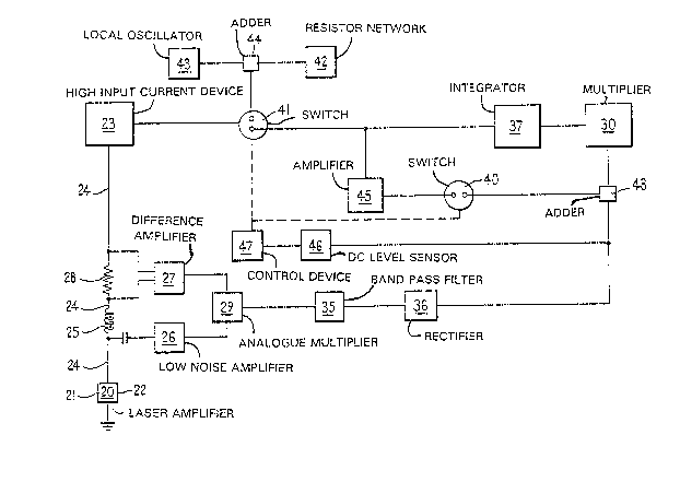
Figure 3 shows a circuit which includes a normal
configuration and a default configuration. The normal
configuration corresponds to an AGC circuit substantially
as shown in ~igure 2. The distress configuration is
o adopted when the control tone falls below a threshold
level.
Loss of control tone is usually caused by a break in
the cable and this prevents normal operation. The de~ault
mode is primarily intended for diagnostic tests. In
particular the default mode indicates a failure at a
particular location or plurality of locations in a long
cable. This gives at least an approximate location of a
fault.
The circuit shown in Figure 3 includes four
sub-circuits, namely:
(1) Normal con~i~urat n
This is slightly modified from the AGC shown in
Figure 2. Elements which perform similar functions have
the same numeral.
(2) Selector
This sub-circuit detects the absence of control tone
(or a signal proportional to the control tone). It holds
the circuit in the normal configuration when the control
tone is above a threshold value and it selects the default
configuration when the control tone is below the threshold
value. The selector includes switches to make the
selection.
(3~ Distress Caller
______
This sub-circuit, which is part oE the default
,.
i
3~
configuration, enables the optical ampl~fier 20 to remain
functional when there is no control tone and it provides a
characteristic frequency to identify itself.
(4) Overload Guard
..
This sub-circuit, which i5 also part of the default
con~iguration, guards against unstable or overloaded
opera~ion when there is no control tone. It i5 desir~ble
to protect against overload when starting operation (for
the first time or after a break) or when operating in
o default mode for diagnostic purposes.
The four sub-circuits will now be described separately.
Item (1) above, ie the AGC, is shown in slightly more
detail than in Figure 2. The extra elements are a band
pass filter 35 to separate control tone from other
frequencies and a rectifier 36 to provide a DC signal to
comparitor 30. The output of the comparitor 30 is
connected to an integrator 37. In the normal
configuration the output of the integrator 37 is connected
to the control port of device 23 via two-way switch 41.
Item (2) above, ie the selector, comprises a DC level
sensor 46 which monitors the output of rectifier 36 and a
control device 47 to actuate switches 40 and 41.
Item 3 comprises a resistive network 42 which produces
a DC bias to substitute for the control signal whenever
the AGC is rendered inoperative by the absence of control
tone. The distress caller also includes a local
oscillator 43 to provide a distress tone characteristic of
its o~l repeater, ie the distress tone is different at
every repeater in the system. Oscillator 43 and resistive
network 42 are connected to an adder 44 which combines the
two signals. The combined signal passes to switch 41
which, in the default configuration, disconnects the AGC
from device 23 and connects the adder 44 to device 23.
- 12 - ~L~ 3~3~
In the default configuration, ie in the absence of
control tone, the ampli~ier 2~ and therefore the
multiplier 29, will have zero input. The comparitor 30
will thus receive a zero input and in conse~uence it will
produce a very high output in an attempt to achieve an
impossible balance. The overload could be enough to
damage itself and subsequent elements, ie the
integrator 37. In the default configuration, the
amplifier 45 feeds back signal from the output of the
integrator 37 to the input of the comparitor 30 with a
gain of, for example, 45dB. This provides a realistic
input signal to the comparitor 30 so that the loop
30-37-45-40-48 stabilises at a safe power. ~The adder 48
prevents detection of the loop signal by sensor 46).
In the normal configuration, the detector 46 actuates
control unit 47 to disconnect the distress caller (42, 43,
44) and the overload guard su~-circuit (45, 40). The AGC
operates as described above. The operation in the default
mode will now be described.
The most usual accident is a broken cable. This
clearly prevents all communication across the break. It
is convenient to call the direction from land to the break
~outward~ and from the break to land "inward~'. Clearly
there are two segments of cable, each with its own inward
and outward direction.
Electrical power to the amplifiers is provided via an
electric conductor included in the optical cable. Even
though the cable is broken it is still possible to provide t
an electrical supply. The sea is utilised as a return
conductor but the broken end does not constitute a short
circuit because the length and electrical resistance af
even the broken segment will be substantial. Thus it is
possible to retain the electrical power whereby the
amplifier can still function.
i
- 12~33~
- 13 -
,
The cable is designed for two directional
communication and each segment will include both inward
and outward telecommunications channels. Clearly the
i outward channels are useless even for diagnoskics. The
s default mode operation of one inward channel will now be
explained.
The amplifier nearest the break will be designated
"first" and its operation will be e~plained first. Even
with the cable broken there is electric power and the
~ amplifier 20 receives a drive current via line 24 but
there are no optical signals received at the input
facet 21 because of the break. Under these conditions the
amplifier will act as an LED so there is an optical signal
at the output facet 22. The mean power of the signal is
set by the control from the network 42, the conditions may
not be optimal but they are at least useful. The local
oscillator imposes its o~n characteristic distress ripple
onto the drive current in line 24 and the optical output
of the amplifier 22 is thereby amplitude modulated at this
characteristic distress frequency.
The modulated LED signal is passed along a fibre to
the next amplifier. There is no control tone so it takes
the default configuration. It is still operational so
that it amplifies its received signal and imposes its own
! 25 characteristic distress frequency from its own local
oscillator. Thus the optical signal produced at the
output facet 22 of the second amplifier is modulated with
two distress frequencies.
The optical signal passes from amplifier to amplifier
whereby, when it reaches land, it is modulated with the
distress frequency of every amplifier in the chain. At
the land station the optical signal is demodulated to an
electrical signal with a complex wave form. This signal
is fed to a frequency analyser which identifies the
3~
- 14 -
distress frequencies present. The presence of a
particular distress frequency indicates that its amplifier
is not only operative in the diskress mode but also that
it is connected to shore and hence the length of the
broken segment can be deduced. Most cables comprise a
plurality of inward channels and the diagnostic tests
described can be repeated for each channel. This gives a
plurality of results which, ideally, confirm one another.
In addition the diagnostic tests can be performed on
o both segments of the cable. This may enable receipt of a
distress frequency from every repeater, some at one end of
the cable and the remainder at the other. This gives a
very clear indication of the location of the breakO
If one segment were very long it might not be possible
to provide electrical power to the outer end without
overloading the inner end. In this case the other segment
would be short and it would be possible to conduct the
diagnostic tests but on the shorter length only.
The overload guard sub-circuit not only protects the
comparitor 30 and integrator 37 during default mode
operation for diagnotic tests as described above but it
also provides a desirable safeguard during the (transient)
period when the cable is switched on. This applies at the
very first switching on and whenever the cable is switched
on after a break in operation, eg after an accident.
Consider the circuit shown in Fiqure 2. Under
electric power and in the absence of optical signal, the
comparitor 30 risks an overload. As shown in Figure 3,
the default configuration ls adopted and this includes
protection against overload.
If an optical signal, with control tone, is provided
to the input facet of Figure 2, then, in the absence of
electric power, there is no amplification and the circ~it
is dead. If power is switched on with signal present
there is no amplification until a suitable drive current
is established in line 24. Furthermore, there will be no
adequate signals to the amplifiers 26 and 27 until this
adequate current is established in line 240
Hence there is a transient period during which the
comparitor 30 and hence device 23 are without proper
control signals. This is an unstable condition with a
potential to overload~ The modification shown in Figure
o protects against this condition. When, because normal
conditions have not yet been attained, there is a low
control signal, the level sensor 46 actuates control unit
47 to keep the circuit in the default configuration. Thus
constant current device 23 has an adequate control signal
lS from network 42 while comparitor 30 and integrator 37 are
protected by amplifier 45. These are stable and safe
conditions for optical amplifier 20 to establish its
function. Level detector 46 reacts when the control
! signal from rectifier 36 becomes adequate and it actuates
control unit 47 to invert switches 41 and 48. This
converts the circuit from its default configuration into
its normal configuration wherein it operates as an ~GC.
This is valuable protection during start up.
It should be noted that level sensor 46 is actuated by
control tone (if present) in both the normal and default
configurations. Thus the circuit switches to default
configuration when control tone drops below the threshold
value and it reverts to normal configuration when the
control tone comes back to values above the threshold.
In normal operation the control tone is substantially
constant after amplification. In default it is zero (or
only noise). Therefore the precise setting of the
threshold value is not important. Settings in the range
25/o to 75/o o~ the normal value are suitable.