Note: Descriptions are shown in the official language in which they were submitted.
g?43 ~0
This invention relates to an electronic connector
capable of having an opposite contact inserted into or
removed from it with a low inserting or removing force or
without inserting or removing force.
Recently, as integrated circuits (such as ICs, LSIs)
have progressed, electronic devices and equipment are
further enhanced in density and are developed in
multifunctions. Thus, the pitch of the contacts of
connectors has been narrowed, and the number of the
contacts has been increased. Here, indispensable problems
arise in which the forces needed for insertion or removal
of electronic parts or circuit boards have increased as
the number of contacts have been increased so that large
forces must be exerted. In other words, even if the
inserting and removing forces for one pair of contacts are
mor~ or less several tens g., when the number of the
contacts increases to several hundreds and or to several
thousands, the inserting and removing forces increase to
several kg. to several tens kg. In this case, when the
components and the boards are inserted or removed by
applying large forces, the terminals of the circuit board
to be inserted or the circuit board itself may be
deformed, damaged or the contacting portion of the contact
of the connector may be damaged or, in the worst case,
broken ~
12~ ~ 3 ~0
The present invention provides an electric connector
comprising: a plurality of resilient contacts associated
in one or more rows in a connector housing, and a shape-
memory spring associated in the connector housing for
driving the contacts, the shape-memory spring, one end of
which is associated with an operation transmitting member
of electrically insulating material and which spring
drives said contacts through said operation transmitting
member, transmitting a recovery force generated when the
shape-memory spring reaches its transformation temperature
or higher to the contacts while recovering the shape
stored and being returned to the shape before its shape-
memory recovery by the spring force of the contact when
the shape-memory spring falls below its transformation
temperature.
BRIEF DESCRIPTION OF THE DRAWINGS
Fig. 1 is a perspective view showing a first
embodiment of an electronic connector according to the
present invention;
Fig. 2 is a cross-sectional view of the first
embodiment;
Fig. 3 is a perspective view showing an example of a
contact of the first em~odiment;
Figs. 4 and 5 are explanatory views showing the
operating state of the first embodiment;
Figs. G and 7 are cross-sectional views showing an
applied example of the f irst embodiment;
Figs. 8 and 9 are partial perspective views of a
shape memory spring used in another applied example of the
first embodiment;
.~
lZ~3 ~0
Fig. 10 is a perspective view showing a second
embodiment of an electronic connector according to the
present invention;
Figs. 11 and 12 are explanatory views showing the
operating state of the second embodiment;
Fig. 13 is a cross sectional view showing a third
embodiment of an electronic connector according to the
present invention;
Fig. 14 is a cross-sectional view of an essential
12~43 ~V
portion of a fourth embodiment of an electronic connector
of the present invention;
Fig. 15 is a cross-sectional view of an essential
portion showing an applied e~ample of the fourth
embodiment;
Figs. 16 and 17 are perspective views showing the
mounting method of a mounting member of Fig. 15;
Fig. 18 is a perspective view showing another example
of the mounting member;
Fig. 19 is a cross-sectional view showing a fifth
embodiment of an electronic connector of the present
invention;
Fig. 20 is a cross-sectional view showing a Sixth
embodiment of an electronic connector of the invention;
Figs. 21 and 22 are explanatory views showing the
operating state of the sixth embodiment;
Fig. 23 is an enlarged view of an essential portion
of a modified example of the si~th embodiment;
Fig. 24 is a perspective view showing a seventh
embodiment of an electronic connector of the invention;
Fig. 25 is a perspective view of a stopper member
shown in Fig. 24;
Figs. 26 and 27 are explanatory views showing the
operating state of the seventh embodiment;
Fig. 28 is a cross-sectional view showing an eighth
embodiment of an electronic connector of the invention;
Fig. 29 is a front view of a contact used in the
eighth embodiment;
Fig. 30 is a front view of a contact used in an
applied example of the eighth embodiment;
-- 4 --
i294~-~0
Figs. 31 and 32 are e~planatory views showing the
operating state of the case that the contact shown in Fig.
30 is used;
Figs. 33 and 34 are cross-sectional views of an
essential portion showing the operating state of a ninth
embodiment of an electronic connector of the invention;
Figs. 35 to 37 are explanatory views showing the
spring force generating state of the contact in the ninth
embodiment;
Fig. 38 is a cross-sectional view showing an
essential portion showing a tenth embodiment of an
electronic connector of the invention;
Fig. 39 is a plan view of an essential portion of the
tenth embodiment;
Fig. 40 is a perspective view of a contact of the
tenth embodiment;
Fig. 41 is a plan view of an essential portion
showing an applied e~ample of the tenth embodiment;
Fig. 42 is a perspective view of the contact of the
tenth embodiment; and
Fig. 43 is a perspective view showing eleventh
embodiment of an electronic connector of the invention.
DESCRIPTION OF THE PREFERRED EMBODIMENTS
Embodiments of an electronic connector according to
the present invention will be described in detail with
reference to the accompanying drawings.
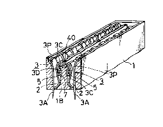
Figs. 1 to 3 show a first embodiment of an electronic
connector of the present invention. As shown in Figs. 1
to 3, the electronic connector of the first embodiment
comprises a connector housing 1 made of an insulating
-- 5 --
12~ ~ 3~
material. The connector housing 1 has two rows of contact
containing chambers 2 opened at its front surface. A
plurality of contacts 3 are contained longitudinally in a
row in an aligned state in each contact containing chamber
2 in such a manner that legs 3A of the respective contacts
3 pass externally through the bottom of the connector
housing 1. Each contact 3 has a contact base portion 3P
and a contact spring portion 3C formed substantially in
U-shape to the contact base portion 3P. A shape memory
spring holding portion 3D is formed, as shown in Fig. 3,
by notching in a tongue shape and erecting the tongue-
shaped portion at the intermediate of the contact spring
portion 3C. Thus, one end of a shape memory spring 5 to
be described later is inserted into the shape memory
spring holding portion 3D of the contact 3 to couple the
shape memory spring 5 to the shape memory spring holding
portion 3D. The shape memory springs 5 are respectively
individually provided at the contacts 3 to be disposed to
individually drive the contacts 3. The shape memory
spring 5 is formed, for example, of nickel (Ni)-titanium
(Ti) alloy or the like, and is formed in U-shaped or V-
shaped cross section. Each shape memory spring 5 is
inserted at its one end into the shape memory spring
holding portion 3D of the contact spring portion 3C to be
connected as described above, and is supported at its
other end to the central partition portion lB of the
connector housing 1 by a cantilever clamp 40. Reference
numeral 7 designates a panellike heater mounted on the
surface of the partition portion lB of the connector
housing 1 for heating the shape memory spring 5.
-- 6 --
1~43 ~0
In the embodiment described above, the transformation
temperature of the shape memory spring 5 is szt to 80~.
Accordingly, the shape memory spring 5 remains~he
martensitic phase at ambient temperatures to be soft and
re/~ ~' ~/7
to be appaL~ t readily plastically deformed. When the
shape me~ory spring 5 is heated to 80~ or higher, the
shape memory spring 5 is transformed into the austenitic
phase to recover the shape stored in advance, thereby
generating a large force at this time.
Figs. 4 and 5 show the operating state of the first
embodiment. When the heater 7 is energized to heat the
shape memory spring 5 to 80~ or higher, the shape memory
spring 5 in the austenitic phase recovers the shape stored
in advance (in this case, the shape memory spring stores
the shape to close both the edges thereof) as shown in
Fig. 4 so that the force generated at this time overcomes
the spring force of the contact spring portion 3C to pull
the contact spring portion 3C. In other words, the
contact base portion 3P and the contact spring portion 3C
are separated therebetween. In this state an opposite
contact 10 can be inserted or removed without an inserting
force or remo~ing force. When the heater 7 is then
deenergized to lower the temperature of the shape memory
spring 5 to ambient temperatures, the shape memory spring
5 in the martensitic phase becomes soft. As a result, as
shown in Fig. 5, the spring force of the contact spring
portion 3C overcomes that of the shape memory spring 5 to
narrow between the contact base portion 3P and the contact
spring portion 3C thersbetween, thereby holding the
opposite contact 10 therebetween by a predetermined spring
-- 7 --
~ 4 3
force.
Whsn the shape memory spring 5 is heated contrary to
the above operation of this e~bodiment, both the edges of
the shape memory spring 5 can be set to open. In this
case, the spring force of the conkact spring portion 3C
overcomes that of the shape memory spring 5 at the ambient
temperatures to press the shape memory spring 5 to the
partition portion lB side as shown in Fig. 4. Since the
interval between the contact base portion 3P and the
contact spring portion 3C is wide at this time, the
opposite contact 10 can be inserted into or removed from
therebetween without inserting force or removing force.
When the shape memory spring 5 is then heated by the
heater 7 to 80~ or higher, the shape memory spring 5
recovers the shape stored in advance (in this case, the
shape memory spring 5 stores the shape e~panding at both
edge thereof) as shown in Fig. 5 to press the contact
spring portion 3C by the recovery force generated in this
case to the opposite contact lo by a predetermined
contacting pressure. In thiS case, the shape memory
spring holding portion 3D may not be provided.
Applied e~amples of this first embodiment is shown in
Figs. 6 and 7. In the applied examples, the contacts 3
and the shape memory spring 5 are constructed the same as
those of the first embodiment except that the shapes of
the contact 3 and the shape memory spring 5 are different
from those of the first embodiment. In these two applied
e~amples, the shape memory springs 5 are set to the state
that the shape memory springs 5 are all noninserting force
or nonremoving force state at ambient temperatures.
-- 8 --
1.2~ 3 ~0
When the shape memory spring 5 is heated in this
state, the shape memory spring reCoVerS the stored shape
and simultaneously pushes the contact spring 3C to press
the contact spring portion 3C to the opposite contact 10.
In the first embodiment shown in Fig. 1, the shape
memory springs 5 are respectively individually provided at
the contacts 3. Thus, there arise problems that the
number of parts increases, and the forces of the shape
memory springs 5 affecting the contacts 3 do not become
lo constant. To solve the problems, the shape memory spring
5 and the contact 3 are insulated therebetween by an
insulating material, and the shape memory spring 5 is
provided commonly for at least two or more contacts 3, and
has a structure that the shape memory spring 5 is
elongated in the direction of alignment of the contacts 3.
ThUs, there are advantages that the number of the shape
memory springs 5 is remarkably reduced, and the spring
force Of the shape memory Spring 5 applied to the contacts
3 becomes constant. ~his modified example is shown in
Fig. 8. Fig. 8 shows only the shape memory spring 5, in
which the other portions thereof are constructed tne same
as those of the first embodiment shown in Fig. 1, and
detailed description of the modified example will be
omitted.
The shape memory spring 5 of the applied modified
example in Fig. 8 is common for at least two or more
contacts 3, and has a structure that the shape memory
spring 5 is elongated in the direction of alignment of the
contacts 3. Further, the sur$ace of the shape memory
spring S is covered with an insulating film 41 to be
described later. Here a method of covering the surface of
the shape memory
spring 5 with the insulating film 41 may spray, for
example, fluoroplastic powder paint or epoxy resin powder
paint on the surface of the shape memory ~pring 5 by
electrostatic painting and then baking the paint. To the
shape memory spring 5 the insulating material such as
polyimide resin, polyester resin, fluoroplastic resin or
vinyl resin may be extruded to be covered, or the surface
of the shape memory spring 5 is covered by bonding an
adhesive such as silicon bond to the inner surface of the
film or glass cloth made of the above-mentioned resin.
The adhesive may use, in addition to the silicon bond,
rubber bond such as SBR ( Styrene-butadine rubber), NBR
(Nitrile-butadiene rubber) or resin bond such as epoxy-
urethane.
In the modified example in Fig. 8, all the surface of
the shape memory spring 5 is covered with the insulating
film 41. However, only the portion to be contacted with
the contacts 3 may be covered with an insulating film 41
as shown in Fig. 9. Or, the portion Of the side of the
contact 3 to be contacted with the shape memory spring 5
iS covered With the insulating film 41 by various methods
as described above.
In the embodiment as described above, the shape
memory spring 5 is formed in a structure that is common
for the contacts 3 and is elongated in the direction of
alignment the contacts 3 and the shape memory spring 5 and
the contacts 3 have electrical insulation therebetween.
Therefore, the spring force generated by the shape
recovery of the shape memory springs 5 to be applied to
the contacts 3 is made constant. Further, the number of
parts can be remarkably reduced. In addition, when such
an electronic connector iS manufactured, sinCe the shape
memory spring 5 iS common for a plurality of contacts 3,
there is an advantage that the shape memory spring 5 is
inserted by being slid from one end to the other of the
connector.
-- 10 --
3 ~0
A second embodiment of an electronic connector of the
invention is shown in Fig. 10. This second embodiment has
the features that a shape memory spring 5 used commonly
for at least two or more contacts 3 and has a structure
that is elongated in the direction of alignment of the
contacts 3, and is disposed at the center of two rows of
contacts 3 to simultaneously drive the contacts 3 of both
the rows. In the second embodiment as shown in Fig. 10,
two rows of a plurality of contacts 3 are associated, and
a U-shaped sectional configuration memory spring 5 is
disposed at the center of the two rows of the contacts 3.
The shape memory spring 5 is inserted at both edges
thereof into shape memory spring holding portions 3D
formed on the sides of the contacts 3. Here, reference
numeral 41 designates an insulating film formed on a
portion of the shape memory spring 5 contacting with the
contacts 3 to insulate the contacts from the shape memory
spring 5 in the same manner as in Fig. 9. Reference
numeral 20 denotes a partition wall, for insulating the
adjacent contacts 3 of the rows, projecting from the
connector housing 1. An attitude holder 42 is placed in
a recess of the shape memory spring 5 to stabilize
the attitude of the shape memory spring 5 to
transmit balanced spring force to the contacts 3 of
both sides. The attitude holder 42 is supported
by the side of the connector housing 1. In this
~Z~3~ 3~0
second embodiment, the transformation temperature of the
sh~pe memory spring 5 is set to 80~. The operation of the
shape memory spring 5 of this case will be described with
reference to Figs. 11 and 12. As shown in Fig. 11, the
spring force of both the contacts 3 overcomes that of the
shape memory spring 5 at ambient temperature time so that
both the contacts 3 are opened at their interval. At this
time, the opposite contact 10 can be inserted or removed
without inserting force or removing force. When the shape
memory spring 5 is then heated by the heater 7 to set the
temperature to 80~ or higher, the shape memory spring 5
tends to recover the shape stored in advance as shown in
Fig. 12 (in this case, the shape closed at both edges of
the U-shape) to pull both the contacts 3 of both sides
inward, with the result that the contacting portions 3B of
the contacts 3 are contacted by a predetermined contacting
pressure with the opposite contact 10.
According to the second embodiment of the invention
constructed as described above, the contacts 3 of the two
rows at both sides of the shape memory spring 5 disposed
at the center can be simultaneously driven, thereby
reducing the number of ~ shape memory s~ g 5.
Fig. 13 shows a third embodiment of an electronic
connector of the invention. The electronic connector of
this third embodiment has a connector housing 1 made of an
insulating material, and the connector housing 1 has a
contact containing chamber 2 opened at the front surface
of the connector housing l. A plurality of contacts 3 are
contained to be in oppositely aligned state in the contact
containing chamber 2 in such a manner that the legs 3B of
- 12 -
43~
the contacts 3 pass externally through the connectorhousing 1 from the bottom. On each sid2 of the housing, a
driving chamber 4 is formed in the connector housing 1
adjacent to the ends of th~ contacts 3, and a U-shaped or
V-shaped memory spring 5 is positioned by a positioning
projection 6 to be contained in each driving chamber 4.
The positioning projection 6 projects from the connector
housing 1. The driving chamber 4 communicates with the
contact containing chamber 2 via a guide ~ having an
opening or a slit. A T-shaped operation transmitting
member 9; is interposed between the shape memory spring 5
and the contact 3. The member 9 transmits a recovery
force generated when the shape memory spring 5 recovers to
the shape stored in advance when the spring 5 iS heated to
the transformation temperature or higher. The operating
transmitting member 9 passes the guide 8, in a manner SO
as to be restricted in its moving direction by the guide
8, i.e., it is restricted to transmit force in a direction
normal to the contact 3.
This third embodiment is an optimum example of an
electronic connector to be used at burn-in testing time
for applying a temperature load as a reliability test for
electronic parts or mounting substrates. In this third
embodiment, the shape memory spring 5 made, for example,
of Ni-Ti alloy is set to 100C as its transformation
temperature. Therefore, in this embodiment of the
electronic connector, the shape memory spring 5 is
martensitic phase at ambient temperature to be soft and to
be apparently readily plastically deformed so that the
spring force of the contact 3 overcomes that of the
.~
3 ~ 0
shape memory spring 5 as shown in the left side in Fig.
13. In other words, the contact 3 presses the operation
transmitting member 9 by its spring force to the driving
chamber 4 side, and the contact 3 is displaced to the
inner wall of the contact containing chamber 2.
Therefore, the opposite contact 10 can be inserted or
removed without inserting force or removing force in this
state. Then, when the electronic connector is inserted
into the burn-in tester in the state that the opposite
contact 10 is inserted and the testing atmosphere reaches
100C or higher, the shape memory spring 5 in the
austenitic phase tends to recover the shape stored in
advance, thereby overcoming the spring force of the
contact 3 by the recovery force generated in this case to
press the operation transmitting member 9 in the
restriction in the direction of the guide 8 as shown in
the right side of Fig. 13. Thus, the contact 3 is pressed
to the center of the contact containing chamber 2.
Therefore, the contact 3 is pressed by the constant spring
force against the opposite contact 10.
In the third embodiment described above, the shape
memory spring 5 and the operation transmitting member 9
may be individually provided corresponding to the contacts
3. In this case, the operation transmitting member 9 may
be formed of an electrically conductive materiaI.
However, it is preferable that the number of
the parts is reduced to simplify the structure and
that the shape memory spring 5 is used commonly
for at least two or more contacts 3 to stabilize
the operation and is elongated in the
- 14 -
~`
lZ~43 ~0
direction of alignment of the contacts 3. In this case,
the operation transmitting member 9 must be composed of an
insulating material as in the third embodiment described
above. Further, this feature is true for all the
following embodiment to be described later. Additionally,
in the third embodiment described above, a plurality of
contacts 3 have been arranged in two rows in an aligned
state. However, this third embodiment can also be applied
to the case of one row of contacts at one side. This
feature is also applicable to all the following
embodiments.
Fig. 14 shows a fourth embodiment of an electronic
connector of the invention. since this fourth embodiment
has a symmetry to the right and left sides, the left side
will be omitted. Even in this fourth embodiment, a
driving chamber 4 which communicates with a contact
containin~ chamber 2 is formed in a connector housing 1
adjacent to the end side of each contact 3. The driving
chamber 4 contains a U-shaped or V-shaped shape memory
spring 5 commonly for at least two or more contacts 3,
i . e., having a structure that is elongated in the
direction of alignment of the contacts 3. Here, the shape
memory spring 5 is buried at its one end in the operation
transmitting member 9 to be connected, and is inserted,
for example, press-fitted at its other end into a groove
11 formed on the connector housing 1 to be connected to
the connector housing 1. Thus, since the shape memory
spring 5 is press-fitted at its other end into the groove
11 of the connector housing 1, the supporting end at
operating time is fixed to reliably transmit the force of
- 15 -
... .
~;~9~3 ~0
the shape memory spring 5 to the contact 3. When the
groove 11 is continuously formed longitudinally of the
connector housing 1, there is an advantage that, after all
the contacts 3 are associated in the connector housing 1,
the shape memory spring 5 connected with the operation
transmitting member 9 can be slid from one end of the
connector in which it is to be mounted.
In the fourth embodiment ~escribed above, when the
atmospheric temperature is lower than the transformation
temperature of the shape memory spring 5, the spring force
of the contact 3 overcomes that of the shape memory spring
5 to press the shape memory spring 5 to the wall side of
the driving chamber 4. In other words, the contact 3 is
displaced to the wall side of the contact containing
chamber 2, and hence the opposite contact 10 can be
inserted without force. When the atmospheric temperature
thereafter reaches the transformation temperature or
higher of the shape memory spring 5, the shape memory
spring 5 tends to recover the shape stored in advance to
transmit the recovery force generated in this case
through the operation transmitting member 9 to the
contact 3, while being supported at its one end by
the groove 11, with the result that the contact 3
is pressed t the center of the contact containing chamber
2 to cause the contacting portion 3B of the contact 3 to
press the opposite contact 10 by a predetermined
contacting pressure. In this fourth embodiment, when
the shape memory spring 5 and the operation
transmitting member 9 are used commonly for at least two
or more contacts 3, the operation transmitting
- 16 -
1~943 ~0
member 9 serves as an insulating member of the contacts 3
and also serves as a member for transmitting the spring
force of the shape memory spring S stably to the contact
3.
In Fig. 14, the operation transmitting member 9 and
the shape memory spring 5 may be connected by providing a
groove to which one end of the shape memory spring 5 is
inserted on the operation transmitting member g and press-
fitting the other end of the shape memory spring 5 to the
grove 11 as the connection of the shape memory spring 5
with the connector housing 1.
When the operation transmitting member 9 is, for
example, formed of thermoplastic resin, one end of the
shape memory spring 5 is inserted in the groove formed on
the operation transmitting member 9, and the groove of the
operation transmitting member 9 made of the thermoplastic
resin is thermally caulked to be fixed. Thus, the
connection of the shape memory spring 5 with the operation
transmitting member 9 can be more reliably executed.
When one end of the shape memory spring 5 is inserted
in the groove 11 formed on the connector housing 1, the
width of the groove 11 must be matched to the thickness,
preferably 0.2 to 0.3 mm, of the shape memory spring 5 so
as to necessarily fix the shape memory spring 5 inserted
to the groove 11, and the width of the groove must be very
narrow. As a result, there arises a problem that
the working of the groove 11 becomes very difficult.
Even if the groove 11 is precisely formed, when
the thin shaped memory spring 5 is press-fitted to
the groove 11, there occurs a danger of deforming
the shape memory spring 5 over the elastic limit
- 17 -
1;~ 9!1 41'3 '~ O
in the worst case. Therefore, as shown in Fig. 15, a T-
shaped mounting member 14 is preferably mounted on one end
of the shape memory spring 5 to be inserted in the groove
11. In this case, the shape of the groove 11 of the
opposite side of mounting is na-turally formed in T-shape.
In Fig. 15, symbol 9A designates a projection formed on
the operation transmitting member 9 to thereby reliably
transmit the force of the shape memory spring 5 to the
contact 3.
Here, the mounting member 14 is mounted on one end of
the shape memory spring 5, as shown, for example, in Fig.
16, by splitting the mounting member 14 into mounting
member pieces 14A, 14B, inserting the projection 15 of one
mounting member piece 14B through a cutout 16 of the shape
memory spring 5 to engage it with the opening 17 of the
opposite mounting member piece 14A to integrate them as
shown in Fig. 17. In this case, the mounting member
pieces 14A, 14B may be bonded by a bond as required.
Further, the mounting member 14 may be formed by inserting
molding on the shape memory spring 5 by direct molding.
Fig. 18 shows another example of a moUnting member 14. In
this case, the mounting member pieces 14 are partially
formed at opposite sides.
When the mounting member 14 is provided at the shape
memory spring 5 in this manner, the groove 11 of the
connector housing 1 is increased in its width, with the
result that the groove 11 can be readily formed.
Since the shape memory spring 5 is mounted in the
groove 11 through the mounting member 14, it is not
necessary to forcibly press it in the groove,
- 18 -
~'.,~
lZ~4L3 ~0
and this avoids the possibility of bending the shape
memory spring 5 oVer its elastic limit. As shown in Fig.
15, when the. section of the mounting member 14 is formed,
for example, in T-shape, there is an advantage that the
shape memory spring 5 is prevented from being removed from
the groove 11. In Fig. 15, only the groove 11 of the
connector housing 1 has been described. However, when the
shape memory spring 5 is inserted into a groove formed on
the operation transmitting member 9, a similar method to
the above method may be applied.
Fig. 19 shows a fifth embodiment of an electronic
connector of the invention. The feature of this fifth
embodiment is different from the third embodiment in Fig.
13 in that the contact 3 and the operation transmitting
member 9 are connected. Here, reference numeral 6
designates a positioning projection for reversely hanging
and positioning a U-shaped or V-shaped shape memory spring
5 to be projected from a connector housing 1. Numeral 7
denotes a heater for heating a shape memory spring 5. The
force of the shape memory spring 5 is restricted in its
direction by a guide 8 having an opening or a slit
through an L-shaped operation transmitting member 9
connected to a contact 3 to be reliably transmitted to the
contact 3. In this fifth embodiment, the transformation
temperature of the shape memory spring 5 is set to 80C.
When the shape memory spring 5 is heated by the
heater 7 to 80C or higher, the shape memory
spring 5 in the austenitic phase tends to recover the
shape stored in advance, thereby overcoming the
spring force of the contact 3 to become the state
o~ the right side in Fig. 19. More specifically, the
-- 19 --
~9~ 3~0
operation transmitting member 9 is pulled by t~e force of
the shape memory spring 5 in a direction restricted by a
guide 8 into a driving chamber 4, thereby pulling the
contact 3 to the driving chamber 4 side. Accordingly, the
opposite contact 10 can be inserted or removed without
inserting or removing force in this state. Then, when the
heater 7 is deenergized so that the temperature in the
driving chamber 4 reaches ambient temperatures, the shape
memory spring 5 becomes the martensitic phase to be soft
and to be apparently readily plastically deformed. Thus,
the spring force of the contact 3 overcomes that of the
shape memory spring 5, the contact 3 is protruded to the
center side of the contact containing chamber 2, and
pressed by a predetermined spring contacting pressure to
the opposite contact 10 inserted by the contacting portion
3B of the contact 3 into the contact containing chamber 2.
Here, when the operation transmitting member 9 is formed
o~ an insulating member such as plastic, the member 9 can
be readily formed, and the shape memory spring 5 and the
contact 3 can be reliably insulated.
Fig. 20 shows a si~th embodiment of an electronic
connector of the invention. In the electronic connector
of this sixth embodiment, a contact containing chamber 2
is opened at the front surface of a connector housing 1
made of an insulating material. A plurality of contacts 3
are associated in two rows in parallel longitudinally in
the contact containing chamber 2. The contacts 3 of two
rows are arranged so that the contacting portions 3B of
the contacts 3 of the two rows are opposed to each other
as pairs, and U-shaped or V-shaped sectional shape memory
- 20 -
~ 3 ~0
spring 5 is disposed to drive the contacts 3 between thecontacts 3 of two rows. Further, the shape memory spring
5 is provided commonly for the contaCts 3 of both side
along the rows to be inserted at both side edges of the
bent recess to grooves 12 formed on operation transmitting
member 9 made of an insulating material to simultaneously
tra.nsmit the tension to the contacts 3 of two rows through
the operation transmitting member 9. The contacts 3 are
partly buried to be connected, for example, in the
operation transmitting member 9 at molding time, and
formed in a structure that the operation transmitting
member 9 is supported midway of the contacts 3. As means
for burying the contacts 3 in the operation transmitting
member 9 may use the above-mentioned molding or means for
press-fitting the contacts 3 to openings formed in advance
on the operation transmitting member 9. In this case, it
is necessary to eliminate a play between the contact 3 and
th~ operation transmitting member 9 to reliably transmit
the force of the shape memory spring 5 to the contact 3.
The material of the operation transmitting member 9 may,
f e_~, ~-,, 7L
for example, preferably employ heat ~4~ fflee resin
having sufficient physical strength under-us~g conditions
such as polyphenylene sulfide, polyetherimide, etc. When
a groove 12 for connecting the shape memory spring 5 to
the operation transmitting member 9 is continuously formed
from one end to the other end of the operation transmitting
member 9, the contacts 3 are associated in the connector
housing 1, the shape memory spring 5 is then preferably
slid from one end to be mounted on the operation
transmitting member 9. In this sixth embodiment, ~he
- 21 -
1~9~3~0
shape memory spring 5 may be bonded by a bond ~o theoperation transmitting member 9 after inserting the shape
memory spring 5 to the groove 12 of the operation
transmitting member 9. The transformation temperature of
the shape memory spring 5 of this si~th embodiment is set
to 80~. When the atmospheric temperature reaches 80~ or
i/? -
higher, the shape memory spring 5 the austenitic phase
generates a large recovery force. The operation of this
sixth embodiment is shown in Figs. 21 and 22. Fig. 21
shows the state of the shape memory spring 5 at a~bient
temperatures. In this state, the shape memory spring 5 is
in the martensitic phase to be soft and to be apparently
readily plastically deformed. The shape memory spring 5
is overcome by the spring force of the contact 3 to be
opened outside by the spring force of the contact 3
through the operation transmitting member 9. In this
state, the opposite contact 10 may be inserted or removed
without inserting or removing force. Then, Fig. 22 shows
the state that the atmospheric temperature becomes
80~ or higher and the shape memory spring 5 becomes the
austenitic phase. In this case, the shape memory spring 5
is recovered to the shape stored in advance, i.e.,
recovered to the shape for closing at both U-shaped or
V-shaped ends to pull the contacts 3 provided in two rows
through the operation transmitting member 9 inside,
thereby generating a predetermined contacting pressure by
the contacting portion 3B of the contact 3 to the opposite
contac~ 10.
This sixth embodiment is designed to obtain a
contacting pressure at high temperature ~me~ However,
- 22 -
1~ 4 ~0
the shape memory spring 5 may be provided to insert orremove the opposite contact 10 without inserting or
removing force by altering the memory shape of the shape
memory spring 5 (e.g., by storing the shape opened at both
ends of U-shape) to generate a predetermined contacting
pressure due to the closure of the contact 3 in such a
manner that the spring force of the contact 3 overcomes
that of the shape memory spring 5 at ambient temperatures,
and recovering the shape stored in the shape memory spring
5 at its transforming temperature or higher to open the
shape memory spring 5 at the outside.
In the sixth embodiment described above, thollgh the
electronic connector has two rows of contacts 3, e~ther
one row of the contacts 3 may be omitted. In this case,
the other end of the shape memory spring 5 is inserted to
the groove 11 formed on the connector housing 1 as shown,
for ~xample, in Fig. 14 or 15.
In the sixth embodiment described above, a method of
mounting the shape memory spring 5 in the groove 12 of the
operation transmitting member 9 may employ a mounting
member 14 as shown in Fig. 23. This is the application of
the method shown in Pig. 15. Thus, the shape memory
spring 5 may not ~e~e from the groove 12 of the
operation transmitting member 9, and there is no
possibility that the inserting end of the shape memory
e ~
spring 5 is excessively bent when ~se~e~.
Fig. 24 shows a seventh embodiment of an electronic
connector of the invention. This seventh embodiment is
modified from the si~th embodiment shown in Figs. 20 to
22. In the sixth embodiment, the operating ranges of the
- 23 -
3 ~0
shape memory spring 5 and the contacts 3 are determined bythe balance of the contacts 3 of the bias spring and the
force of the shape memory spring 5 with the result that
there is a problem that the contacts 3 cannot be
accurately controlled in positioning. In other words,
when considering the repetitive fatigue of the shape
memory spring 5 and the contacts 3 and the requirement for
a predetermined amount of deformation over a long period,
it is necessary to accurately manage the strain amount and
to use the spring 5 and contacts 3 in a range that the
strain amount may not exceed a predetermined value. Thus,
in Fig. 24, an inner wall lA of a connector housing 1 is
provided for restricting the outward operation range of
the operation transmitting member 9 is formed at one side
of the operation transmitting member 9 in the operating
direction (lateral direction in Fig. 24), and a stop
member 13 is formed to restrict the operating range in the
other or inward direction. In the seventh embodiment
described above, the stop member 13 and partition walls 20
are connected by a connecting portion 13A as shown in Fig.
25 to be positioned and contained in a contact containing
chamber 2. The stop member 13, the connecting portion 13A
and the partition wall 20 may be integrally formed with
the connector housing 1, or the partition 20 may be
integrally formed with the connector housing 1, and the
stop member 13 may be directly connected to the
longitudinal side of the connector housing 1. Figs. 26
and 27 are cross-sectional views showing the
operation of the seventh embodiment. Fig . 2 6 shows an
arrangement different from the case of Fig. 20, that
- 24 -
3-~0
when the electronic connector is at high temperature, the
opposite contact lo can be inserted into or removed
without inserting or removing force. At ambient
temperature, the shape memory spring 5 in the martensitic
phase is soft and apparently readily plastically deformed.
Thus, the force of the shape memory spring 5 is overcome
by the spring force of the contact 3 to be inwardly
pressed through the operation transmitting member 9. At
this time, the operation transmitting member 9 is
contacted with the stop member 13 to stop movin~ inwardly.
In Fig. 26, the opposite contact 10 is omitted. However,
the contact 3 and the opposite contact 10 are contacted in
this state. Then, when the heater 7 disposed between the
connector housing 1 and the shape memory spring 5 is
energized to heat the shape memory spring 5 to the
transformation temperature or higher, the shape memory
spring 5 is transformed to the austenitic phase to tend to
recover the shape stored in advance (in this case, the
shape opened at both side U-shaped ends is stored),
thereby expanding the contacts 3 through the operation
transmitting member 9 as shown in Fig. 27. At this time
the operation transmitting member 9 is contacted with the
inner wall lA of the connector housing 1 to stop moving
outward. Accordingly, even if the shape memory spring 5
generates spring force more than required at this time, a
large strain is not applied to the contact 3. The
opposite contact 10 not shown in this state can be
inserted or removed without inserting or removing force.
In the seventh embodiment described above, when the
shape for closing both ends is stored in the shape memory
- 25 -
~`
3 10
spring 5, when the shape memory sprin~ 5 reaches its
transformation temperature or h:igher, the shape memory
spring 5 can operate reversely to the manner described
above with reference to Figs. 26 and 27.
In the seventh embodiment described above, either one
row of contacts 3 may be omitted similarly to the case of
the sixth embodiment. In this case, the other end of the
shape memory spring 5 is inserted fixedly to a ~roove 11
formed on a connector housing 1 as shown, for example, in
Figs. 14 and 15.
Fig. 28 shows an eighth embodiment of an electronic
connector of the invention. This eighth embodiment is
modified and improved from the sixth embodiment in Fig. 20
and the seventh embodiment in Fig. 24. More specifically,
in the sixth embodiment, the shape memory spring 5, when
exposed to a high temperature atmosphere, takes several
tens seconds to reach its transformation temperature, and
even a simple continuity check cannot be executed at the
opposite contact 10 side during the period. In the
seventh embodiment~ when the energization of the heater 7
is stopped, it takes a considerable time to generate a
contacting pressure between the contacts 3 and the
opposite contact 10 due to the narrow interval of the
contacts at both sides aligned in two rows as shown in
Fig. 26 until the temperature of the shape memory
spring 5 falls below its transformation temperature.
In this case, the continuity test cannot be
performed as described above. In other words, in
the above-mentioned embodiments, it takes several
tens of seconds to transform the shape memory
spring 5, and there is a problem that even a simple
- 26 -
~ 3~0
initial check cannot be executed during the period.
Therefore, the eighth embodiment has a feature that an
initial check such as a continuity check can be executed
during the period until the shape memory spring 5 is
transformed to the desired phase. In this eighth
emb~diment as shown in Fig. 28, the contacts 3 have weak
spring force auxiliary contacting portions 3E which stand
by at positions to contact before a strong spring force
main.contacting portion 3B contacts the opposite contact
10. ~This weak spring force auxiliary contacting portion
3E is formed with a narrow auxiliary spring portion 24 so
that a slit 23 is formed from the upper portion toward the
~,, ~
lower portion to boce~e a weak spring force as shown in
Fig. 29, and the au~iliary spring portion ~4 is e~tended
to the center of the,contact containing chamber 2 as shown
in Fig; 28.
In the electronic connector of the eighth embodiment
e ~,~f~
described above, when the shape memory spring 5 booomcs,
for example, the martensitic phase, the weak spring force
au~iliary contacting portion 3E is extended inward to
stand by. Accordingly, the opposite contact 10 can
contact the weak spring force au~iliary contacting portion
3E before contacting the strong force main contacting
portion 3B, and even if the shape memory spring 5 is not
transformed to the austenitic phase, i.e., is not heated,
the initial check can be executed. When the shape memory
spring 5 is heated to be transformed to the austenitic
phase, the contact 3 is moved to the center of the contact
containing chamber 2 through the operation transmitting
member 9 by the force of the shape memory spring 5, and the
- 27 -
~ 4 3~0
strong spring force main contacting portion 3B iscontacted with the opposite contact 10. More
particularly, in Fig. 28, the shape memory spring 5 is the
martensi~ic phase at ambient temperature, and is stopped
in,balance with the contact 3. Since the strong spring
force main contacting portion 3B is disposed steadily at
the position slightly retreated with respect to the
opposite contact 10 from the weak spring force auxiliary
contacting portion 3E at this time, only the weak spring
force auxiliary contacting portion 3E is contacted when
the~opposite contact 10 is inserted. Thus, the opposite
contact 10 can be inserted with extremely weak force. The
necessary minimum contacting pressure is generated for an
initial check at this time. After the initial check is
completed, when the shape memory spring 5 arrives at high
temperature 4~ uEing ~te, the shape memory spring 5 is
transformed to the austenitic phase, becoming the stored
shape, i.e., the state as shown by broken lines in Fig.
28. As a result, the strong spring force main contacting
portion 3B is contacted with the opposite contact 10 by
large contacting pressure, and high reliability is
obtained even in ~e continuous usage at high temperature.
When returned again to ambient temperature, the shape
memory spring 5 is stopped at the position designated by
solid lines in Fig. 28, and the opposite contact 10 and
the contact 3 are contacted only ~ the weak spring force
auxiliary contacting portion 3E.
Even in~case of an electronic connector used at
ambient temperature, when this contact 3 is applied, the
initial check can be e~ecuted immediately after the heater
- 28 -
3 ~(~
7 is deenergized, and a high contacting pressure is
obtained when the temperature falls below the
transformation temperature of the shape memory spring 5.
Fig. 30 shows another modified example of this eighth
embodiment. The contact 3 is different from that in Fig.
29, in that a slit 23 is formed from the upper portion to
the lower portion of the contact 3 to form an auxiliary
spring portion 24. Thus, a weak spring force ~uxiliary
contacting portion 3E is stopped at a predetermined
position substantially irrespective of the movement of the
strong spring force main contacting portion 3B driven by
the shape memory spring 5 which may be similar t~ that in
Fig. 17. An example of using the contact 3 is shown in
Figs. 31 and 32. This electronic connector is used at
ambient temperature. In this example, the outwardly
pulling force of the shape memory spring 5 in the
austenitic state heated by the heater 7 aS shown in Fig.
31 iS transmitted through th2 operation transmitting
member 9 to the ContaCt 3, and the Strong spring force
main contaCting portion 3B of the ContaCt 3 iS pulled to
the inner wall side of the ConneCtor housing 1. In this
state, only the weak spring force auxiliary contacting
portion 3E remains at the center of the contact containing
chamber 2 to stand by. Accordingly, the opposite contact
is contacted with the weak spring force auxiliary
contacting portion 3E by weak contacting pressure.
Therefore, an initial, check can be executed by the weak
spring force auxiliary contact 3E during several tens
seconds before the heater 7 is stopped and the shape
memory spring 5 is returned to the martensitic phase.
~fter the several tens second, the shape memory spring 5
is returned to the martensitic state. Then, as shown in
Fig. 32, the spring force of the contact 3 overcomes the
spring force of the shape memory spring 5 to return to the
- 29 -
, ,j.
"~
3~0
center of the contact containing chamber 2, with the
result that the contacting pressure of the strong spring
force main contacting portion 3B is added to the
contacting pressure of the weak spring tension auxiliary
contacting portion 3E to act a large contacting pressure
on the opposite contact 10.
Figs. 33 to 37 show a ninth embodiment of an
electronic connector of the invention. Th~ eighth
embodiment in Fig. 28 forms the auxiliary spring portion
24 by forming the slit 23 on the contact 3, while the
ninth embodiment is improved to provide the same
advantages as those in the eighth embodiment by one
contact 3. The portions except the contact 3 are
constructed fundamentally the same as the sixth embodiment
in Fig. 20, and only the feature of the ninth embodiment
will be shown and described. In the ninth embodiment, the
contact 3 is composed of a contact weak spring portion 3F
erected from the bottom of a connector housing 1 in a
contact containing chamber 2 so that the upper end side is
bent in a predetermined radius of curvature downward, and
a contact strong spring portion 3G is formed integrally
with the end of the contact weak spring portion 3F and is
bent in a V-shape. The contacting portion 3B is formed at
a boundary between the contact weak spring portion 3F and
the contact strong spring portion 3G. A blocklike
operation transmitting member 9 is formed on a portion of
the contact weak spring portion 3F corresponding
approximately in height to the ......
- 30 -
43~(~
contact strong spring portion 3G. One end of the shape
memory spring 5 is press-fitted to the groove 12 of the
operation transmitting member 9. An engaging bent portion
3K is formed as a substantially perpendicular bend at the
end of the contact strong spring portion 3G. The engaging
bent portion 3K is placed on the upper surface of the
operation transmitting member 9.
In the electronic connector of the ninth embodiment
described above, when the atmosphere is at ambient
temperature and the shape memory spring 5 is in the
martensitic state, the contacting portion 3B is disposed
steadily at a position contacted when the opposite contact
10 is inserted as shown in Fig. 33. In this state, the
spring force at load acting point 3H of the black solid
portiQn of the contact weak spring portion 3F in Fig. 35
is balanced with the force of the shape memory spring 5.
Then, when the opposite contact 10 is inserted as shown in
Fig. 36, the contacting portion 3B is pressed back to the
surface line of the opposite contact 10 to generate a
predetermined weak contacting pressure in which state an
initial check can be executed. At this time, the spring
force of the contact 3 effecting the contacting pressure
is generated at the portion of the contact weak spring
portion 3F shown in black solid portion in Fig. 36. The
stiffness at this time is that generated by the contact
weak spring portion 3F which is Very weak as compared with
that of the state of Fig. 37 described later, and even if
the position of the contacting portion 3B is slightly
displaced, the contacting pressure does not alter to a
great extent.
When the electronic connector of this ninth
embodiment is exposed to a high temperature i.e., the
transformation temperature or higher of the shape memory
spring 5 after the opposite contact 10 is inserted, the
shape memory spring 5 in the austenitic phase overcomes
the spring force of the contact 3, tends to recover to the
- 31 -
43 ~()
stored shape, thereby stopping steadily in the state in
Fig. 34. As a result, the contacting point 3B contacts
the opposite contact 10 with a large contacting pressure
to obtain a high reliability in the continuous operation
at high temperature. At this time, the spring force Of
the contact 3 effecting the contacting pressure is
initially generated by the contact weak spring portion 3F
shown in black solid in Fig. 36, but as the shape memory
spring 5 recovers in its shape, the spring force of the
contact 3 is generated by the operation transmitting
member g contacting with the oblique surface of the
contact strong spring portion 3G as shown in both the
black solid portion and in the hatched portion in Fig. 37.
The load acting point at this time becomes the two points
3H and 3M in Fig. 37, and particularly the black solid
portion provides high stiffness for the contact strong
spring portion 3G, and the shape recovering force of the
shape memory spring 5 is transmitted to the contacting
portion 3B substantially as it is.
In the electronic connector of this ninth embodiment
of this type, it is preferable to deform the contact 3 as
little as possible, i.e., to increase the stiffness so as
to utilize the force of the shape memory spring 5 as the
contacting pressure, but when it is, on the contrary,
necessary to contact the opposite contact lo with the
contact 3 by weak spring force for the purpose of initial
check, the stiffness of the contact 3 i~ p~eferably
smaller. In the ninth embodiment, this requirement is
satisfied by altering the stiffness at the load acting
point of the contact 3 during the period in which the
shape memory spring 5 is brought into effect upon rising
of the temperature after the opposite contact 10 is
inserted.
The opposite contact 10 is wiped on the surface by
the contacting portion 3B of the contact 3 when the
opposite contact 10 is initially inserted, but in this
- 32 -
1~94~
ninth embodiment, the contacting point of the contacting
portion 3B and the opposite contact lo is not altered
significantly during the series of operations of the
contact 3 and the shape memory spring 5 described above.
Therefore, a contact of extremely high reliability is
obtained from the electric point of view.
When using the connector at ambient temperature, the
transformation temperature of the shape memo~y spring 5 is
set to a low tempera~ure such as 0C, and when the
opposite contact 10 is inserted, the electronic connector
is cooled. Then, similar effects to those described above
are obtained. In the ninth embodiment described above,
this can be applied to both one and two rows of the
contacts 3 in the same manner as the embodiment described
above.
According to the ninth embodiment described above,
dlfferent from th~ eighth embodiment, the contact 3 is
composed of the contact weak spring portion 3F and the
contact strong spring portion 3G, and the contacting
portion 3B is formed at the boundary between the spring
portions. The memory recovery force of the shape memory
spring 5 acts through the operation transmitting member 9
to the contact strong spring portion 3G~ and the
contacting portion 3B is disposed at a position capable of
contacting the opposite contact 10 when inserted in the
stand-by state. Therefore, the contacting portion 3B
extended to the line of insertion of the opposite contact
10 is supported by the contact weak spring portion 3F at
the initial check time and there is the advantage that it
resists With weak force when pressed so that the initial
check can be executed employing extremely weak inserting
or removing force. When the shape memory spring 5 is
operated, the force of the shape memory spring 5 acts
through the operation transmitting member 9 to the contact
strong spring portion 3G of the contact 3. Thus, the
attenuation of the force of the shape memory spring 5 is
~. .
lZ~43 ~0
minimized to transmit the force of the shape memory spring
S to the contacting portion 3B to obtain a contacting
pressure different from that achieved with the contact
weak spring portion 3F. Further, different from the
embodiments described above, this ninth embodiment has the
advantage that the surface of the opposite contact 10 is
wiped when the opposite contact 10 is inserted regardless
of the state of the shape memory spring 5.
Figs. 38 to 40 show a tenth embodiment of an
electronic connector of the invention. This tenth
embodiment is improved to accurately control the position
of the operating range of the contact 3 in the ninth
embodiment for the purpose of improving fatigue
characteristics by eliminating the strain on the contact 3
exceeding a predetermined amount.
In the tenth embodiment, the electronic connector
has a symmetry at right and left sides, and left half will
be omitted for the clarity of the drawings and the
description. Since the essential portion of the tenth
embodiment is substantially the same as that of the ninth
embodiment in Figs. 33 to 37, the description of the same
portions will be omitted.
In Figs. 38 to 40, a first restricting portion 30
made of a projection for restricting the operating range
of the contact 3 is formed on the side of the folded
portion 3N of the contact weak spring portion 3F of the
contact 3. A second restricting portion 31 provided by a
recess for restricting the operating range of the contact
3 in cooperation with the first restricting portion 30 is
formed correspondingly on the partition wall 20 between
the contacts 3. The first and second restricting portions
30, 31 cooperate with one another to restrict the
operating range of the contact 3.
In the electronic connector of the tenth embodiment
- 34 -
~^
129~3'~0
described above, when the opposite contact 10 is inserted
at ambient temperature, the first restricting portion 30
stops at the stop surface 31B of the second restricting
portion 31 to always exert a predetermined contacting
pressure. The shape memory spring 5 recovers in a
direction such that the shape memory spring 5 is
contracted inward at high temperature i.e., at the
transformation temperature or higher of the shape memory
spring 5. In this case, even if the shape memory spring 5
produces more force than required, the contact 3 is
contacted at the first restricting portion 30 with the
stop surface 31A of the second restricting portion 31 to
be restricted. Thus, the strain imposed on the contact 3
does not exceed a critical limit.
Figs. 41 and 42 show an applied example of the tenth
embodiment. This applied example is different from the
tenth embodiment in that a first restricting portion is
formed with a recess and used at both ends as stop
surfaces 30A, 30B and a second restricting portion 31 is
formed with a projection.
In the electronic connector of the applied example of
the tenth embodiment described above, the contact 3
overcomes the spring force of the shape memory spring 5 at
ambient temperature to tend to open outward, but the stop
surface 30A contacts the second restricting portion 31 to
stop, thereby providing a predetermined contacting
pressure when the opposite contact 10 is inserted. When
the atmospheric temperature rises to the transformation
temperature or higher of the shape memory spring 5, the
spring force of the shape memory spring 5 overcomes the
spring force of the contact 3 to cause the shape memory
spring to recover in an inwardly contracting direction.
Even if the opposite contact 10 is not inserted, the stop
surface 30B of the first restriction portion 30 formed on
the contact 3 is stopped by the second restricting portion
31 formed on the partition wall 20 to avoid the critical
- 35 -
1?~ ~ 3 ~
strain o~ the contact 3 being exceeded. When there is a
facing contact 3, i.e., when the contacts 3 are opposite
in two rows, it prevents the facing contacts 3 from
contacting with one another. In the tenth embodiment, the
electronic connector has been u5ed at the high
temperature. However, in the case in which the electronic
connector is to be used at amblent temperature, the
transformation temperature of the shape memory spring 5 is
set, for example, to ooc, the electronic connector is
cooled before the opposite contact 1o is inserted, and it
may be exposed t~ the ambient temperature after the
opposite contact lo is inserted. Or, a heater is
associated in the contact containing chamber 2 of the
connector housing 1, and before the opposite contact 10 is
inserted, the heater is energized, and the contact 3 is
opened by the shape memory spring 5 in which has been
stored in advance a shape so that both ends of its U-shape
are opened to allow insertion or removal of the opposite
contact 10 without inserting or removing force. When the
energization of the heater is stopped after the opposite
contact 10 is inserted, sufficient contacting pressure can
be obtained at ambient temperature.
Fig. 43 shows an eleventh embodiment of an electronic
connector of the invention. In the eleventh embodiment,
in an electronic connector of the type in which U-shaped
open edges of a shape memory spring 5 are press-fitted to
grooves 12 formed on an operation transmitting member 9,
an arrangement is provided for preventing the shape memory
spring 5 from disengaging from the groove 12 of the
operation transmitting member 9. In other words, an
elastic member 35 is provided between the shape memory
spring 5 and the connector housing 1, and the shape memory
spring 5 is urged by the elastic member 35 in the
direction of the groove 12 of the operation transmitting
mem~er 9. As a result, there are advantages that the
shape memory spring 5 is prevented from disengaging from
the groove 12 of the operation transmitting member 9 and
- 36 -
1~4~ ~0
the operating point of the shape memory spring 5 is
stabilized. When the elastic member 35 is mounted in a
structure where no heater 7 is provided in the electronic
connector, similar to the structure described above with
reference to Fig. 13, the elastic member 35 is inserted
between the shape memory spring 5 contained in the driving
chamber 4 and the bottom of the driving chamber 4, and the
shape memory spring 5 is pressed by the elastic member 35
to the grove 12.
With the electronic connector constructed as
described above in accordance with the invention, it will
be appreciated that the opposite contact can be inserted
or removed without or with low inserting or removing
force. The electronic connector of the invention provides
simple structure and high reliability. Further, in the
preferred form, an initial check can be executed as
required.
- 37 -