Note: Descriptions are shown in the official language in which they were submitted.
-- 1 --
PROCESS FOR THE PRODUCTION OF OPTICAL ELEMENTS
BACKGROUND OF THE INVENTION
1. Field of the Invention
The present invention relates to a process for the
production of an optical element such as a lens, gradient
thickness film, or the like. More particularly, the
present invention relates to a process for the production
of plastic microlenses and the arrays thereof, optical
waveguides, diffraction gratings, holograms, and the like.
The present invention also relates to an optical device
using the optical element of the present invention.
Microlenses or micro optical lenses have various uses.
For example, they can be used in the ramification and
combination of lights and the mixing and branching of waves
in fiber optics communication, the condensation of lights
in optoelectroluminescence devices and light emitting
diode-sensor arrays, and as a waveguide lens for integrated
optical circuits. Preferably, these microlenses, etc.,
have a short focal length, when used for the above
purposes. Further, optical waveguides and diffraction
gratings should show a negligible optical transmission loss
and a good diffraction efficiency, respectively.
2. Description of the Related Art.
Hitherto, in the production of microlenses and arrays
thereof, made from inorganic materials or plastic
materials, the following methods have been principally
used:
Ion Exchange Method:
Briefly, this method will be described with reference
to the production of a flat plate-type
.~
microlens. In this method there is provided a glass
substrate with a mask thereon, the mask having an opening
through which a dopant is permitted to diffuse onto a
substrate, to increase a refractive index o~ the substrate.
The highest concentration of dopant is around the opening
of the mask and it gradually decreases in depth and radius
directions.
Suspension Polymerization Method:
This method is not illustrated herein, but is useful
in the production of, for example, distributed index- or
gradient index-type cylindrical or spherical lenses. These
lenses can be produced by the suspension polymerization of
polymerizable materials, and are characterized by a
continuously varied refractive index.
Electron Beam (EB) Patterning Method:
The EB method is used to produce, for example, Fresnel
lens arrays. First, a transparent electrically conductive
coating, which is used to prevent an accumulation of
electric charges during the EB patterning, and an EB resist
coating are deposited, in that order, onto a glass
substrate. The deposited resist coating is then subjected
to EB exposure using an electron beam. The EB exposure of
the resist coating is carried out in such a manner that the
strength of the exposure corresponds to the desired pattern
of the cross-section of the Fresnel lens arrays. After the
exposure is completed, the exposed resist coating is
developed with a developer, and Fresnel lens arrays are
obtained.
Casting Method:
According to this method, the lens-forming materials
are introduced in a mold and cast therein.
-- 3
This method can be used in the production of, for
example, flat convex lenses and Fresnel lenses.
However, these prior art methods have several
disadvantages. Namely, the ion exchange method is
disadvantageous because it can not provide a microlens
with a reduced aperture, the focal length of the lens
can not be freely varied,- and the resulting lens can not
be laminated on other optical devices. The suspension
polymerization method is not suitable in the production
of lens arrays, because in this method, each lens of the
arrays must be produced separately, which increases
production costs. The EB patterning method suffers from
drawbacks such as a large chromatic aberration, small
condensing rate, lower mass-production capability, and
high costs. Further, in the casting method, it is
difficult to micronize the resulting lens and to inte-
grate the same with other optical devices.
Therefore, a novel method for producing
optical elements such as convex or concave microlenses
and arrays thereof is needed, which method enables the
production of elements micronized in size and capable of
integration with other optical devices, on a mass-
production scale and at a low production cost.
In addition to the microlenses and arrays
thereof, other types of optical elements such as gradient
thickness films, for example, optical waveguides,
diffraction gratings, and holograms have been produced
using the method described above, or hy other methods.
The gradient thickness films or films with a distributed
thickness can be produced, for example, by selectively
exposing a film having a photoreactive compound uniformly
dispersed therein, to produce a distribution o the
reaction product of the photoreactive compound, and then
annealing the coating to remove the unreacted photo-
reactive compound. This method is utilized in theproduction of the optical waveguides. Another method is
utilized in the formation of, for example, holograms. A
-- 4
common drawback to these prior art methods is tha~
variations in the configuration of the film are very
small, because these methods were originally intended to
convert a distribution of lights or exposure intensity
to a distribution of the density or refractive index of
the film. Desirably, in the production of the gradient
thickness films, variations in the configuration of the
film are increased.
SUMMARY OF THE INVENTION
According to the present invention, there is
provided a process for the production of an optical
element, which comprises the steps of:
forming on a substrate a light-sensitive film
containing at least a photoreactive compound capable of
causing a migration of unreacted compound from an
unexposed area to an exposed area as an exposure func-
tion, thereby changing a configuration of e~posed
light-sensitive film, and
selectively exposing the light-sensitive film
to obtain an optical element having a desired configu-
ration.
The optical element producea according to the
present inven~ion includes a variety of optical products
such as microlenses and arrays thereof, for example,
convex or concave lenses, distributed index lenses, and
Fresnel lenses; optical waveguides; diffraction gratings;
holograms, and the like. The type of optical products
included in the term "optical element" used herein will
be clarified by the following description with respect
to preferred embodiments of the present invention.
According to the present invention, ~here is also
provided an optical device which comprises a support or
substrate having a shadow mask which acts to prevent
visible light from go through an area of a film where no
lens is, and an optical lens formed sequentially thereon.
In the optical device according to the present
invention, the optical element such as a microlens or an
3LZ~ Lffl'~
-- 5 --
array thereof is produced in accordance with the present
process. The shadow mask is, therefore, a part or all
of the photo mask used in the present process.
BRIEF DESCRIPTION OF THE DRA~INGS
Figure 1 is a perspective view showing a prior art
method for producing a flat plate-type microlens;
Fig. 2A is a perspective view showing another prior
art method for producing Fresnel lens arrays;
Figs. 2B and 2C are cross-sectional views illustrat-
ing, in sequence, the method of Fig. 2A;
Figs. 3A, 3B, and 3C are cross-sectional views
illustrating, in sequence, the production of convex
microlens arrays according to the present invention;
Figs. 4A and 4B are photographs showing plane and
cross-sectional views of the convex microlens according
to the present invention;
Figs. 5A and 5B are photographs showing the convex
microlens arrays according to the present invention and
the use thereof;
Figs. 6A to 6E are cross-sectional views illus-
trating, in sequence, the process of the formation of
the lens upon exposure;
Fig. 7 is a diagram showing a mechanism of the
formation of the lens according to the present invention;
Fig. 8 is a cross-sectional view showing a mechanism
of the formation of the lens according to the present
invention;
Fig. 9 is a graph showing a relationship between
the thickness of the film and the diameter of the lens
pattern;
Fig. 10 is a graph showing the relationship between
the concentration of cinnamyl chloride and the diameter
of the lens pattern;
Fig. 11 is a graph showing the relationship between
the exposure time and the focal length;
Figs. 12A to 12C are cross-sectional views illus-
trating, in sequence, the lens formation process accord-
~2~47~)
.
-- 6 --
ing to another embodiment of the present invention;
Fig. 13 is a cross-sectional view showing a modifi-
cation of the optical device of Fig. 12C;
Figs. 14A to 14C are cross-sectional views illus-
trating, in sequence, the lens formation process accord-
ing to still another embodiment of the present invention;
Figs. 15A and 15B illustrate the production of the
concave lens arrays according to an embodiment of the
present invention;
Figs. 16A and l~B illustrate the production of the
concave lens arrays according to another embodiment of
the present invention;
Fig. 17 is a graph showing the relationship between
the exposure time and the variation of the film thick-
ness;
Figs. 18A and 18B illustrate the production of thegradient thickness films according to still another
embodiment of the present invention;
Fig. 19 is a schematic view showing a principle of
the production process of Figs. 18A and 18B; and,
Figs. 20A and 20B illustrate the production of the
gradient thickness films according to still another
embodiment of the present invention.
DESCRIPTION OF THE PREFERRED EMBODIMENTS
In the method of the present invention, a photo-
reactive compound which exhibits a specific behavior
upon exposure to radiation is added to a light-sensitive
film in which the intended optical element is formed.
This exposure causes substantial differences between the
exposed area and the unexposed area in the melting
point, diffusibility, evaporation pressure, molecular
size and weight, and the like of the photoreactive
compound. Subsequently, migration of the unreactQd
photoreactive compound from the unexposed area to the
exposed area occurs, changing the configuration of the
exposed area of the light-sensitive film. The micro-
lenses are finally obtained when a surface tension and
~2~4~
-- 7
similar forces act on the exposed film.
Any photoreactive compound can be used in the
practice of the present invention, so long as the
compound can produce the above-descrihed actions.
Useful photoreactive compounds are those which are
capable of inducing polymerization, cross-linking,
isomerization or other photoreactions. The term
"polymerization" or "photopolymerization" has a broad
meaning herein, and includes oligopolymerization or
low-order polymerization ~or use in the formation of
oligomers such as dimer, trimer and the like, homopolyme-
rization, copolymerization, and similar polymerizations.
Typical examples of the photoreactive compounds
useful in the present invention are:
(1) Photopolymerizable materials
1) with cyclic addition reaction
R2 R5
C C R - _ R
~ hv ~ 1 6
C ~C R3 - _ - R8
3 4 R7 R8 4 7
i.) cinnamic acid and esters thereof
(Rl = R5 = phenyl, R2 ~ R3 = R6 I R7 Y g
R4 = R8 = COOR, R = hydrogen, alkyl, substituted
alkyl and ~imilar substituents); For example:
cinnamic acid
~ -CH: CHCOOH
methyl cinnamate
r~
~ CH: CHCOOCH3
ethyl cinnamate
~ CH: CHCOOC2H5
vinyl cinnamate
~ -CH: CHCOOCH = CH2
allyl cinnamate
~ CH: CHCOOCH2CH = CH2
-- 8 --
cinnamyl cinnamate
~ CH: CHCOOCH2CH: CH
glycol cinnamate
~ CH: CHCOO(CH2)nOCOCH: CH
benæyl cinnamate
~ CH: CHCOOCH
ii.) carboxylic acid cinnamyls (R
= R5 = phenyl, R2 ~ R3 = R6 ~ R7 = hydrogen'
R4 = R8 = CH20COR); For example:
dicarboxylic acid cinnamyl
~ CH: CHcH2oco(cH2)ncoocH2cH
CH ~ ; methacrylic acid cinnamyl
CH2 = C(CH3)COOCH2CH CH
iii.) others
~-methyl cinnamic acid
~ CH: C(CH3)COOH
p-methyl cinnamic acid
H3C ~ ~CH: CHCOOH
cinnamyl chloride
~ CH: CHCOCl
2) with chain-like addition reaction
\ / C 12 4 16 18
/C\ /C ~ - C - C - C - C -
R3 4 R7 R8 Rl R8 R5 R7
i.) acrylic acid esters represented by
CH2: CHCOOR selected from epoxy-, urethane-, acryl-
and amine-type esters; For example:
m-phenylene diacrylic acid ester
ROCOCH = CH ~ CH: CHCOOR'
ii.) methacrylic acid esters represented
by H3CCH: CHCOOR selected from epoxy-, urethane-,
acryl- and amine-type esters; For example:
methyl methacrylate
3~ 3
H3CCH: CHCOOCH3
iii.) others
(2) Isomerization materials
i) cyclization materials
Stilbene
~ CH = CH
ii) others
(3) Other materials which are based on the above
materials (1) and/or (2) and, further:
10i) which contain one or more photofunctional
groups,
ii) which contain two or more of the same or
different functional groups,
iii) which are monomers, oligomers including5 copolymers, or blends thereof,
iv) which are blends of different molecules,
and
v) which are reacted upon irradiation of
ultraviolet rays, visible rays, heat rays, and other0 radiation.
These photoreactive compounds may be used alone or
in combination, depending upon the desired results and
other factors, and may be also used in combination with
other materials such as binding polymers as a binding
agent and solvent.
Typical examples of useful binding polymers are:
(1) polyacrylic acid esters
i) polymethylacrylate
ii) polymethyl-a-bromoacrylate
30(2) polymethacrylic acid esters
i) polymethylmethacrylate
ii) polyphenylmethacrylate
iii) polypentabromophenylmethacrylate
iv) polypentachlorophenylmethacrylate
35v) polyisobutylmethacrylate
vi) polytrifluoroethylmethacrylate
(3) styrene polymers
~Z~7~
-- 10 --
i) polystyrene
ii) poly o-chlorostyrene
(4) carbonate polymers
i) polycarbonate
ii) diethylene glycol allylcarbonate polymer
(trade name: CR-39)
t5) vinyl polymers
i) polyvinyl benzoate
ii) polyvinyl acetate
iii) polyvinyl carbazole
iv) polyvinyl naphthalene
v) polyvinyl butyral
(6) others
i) polyacrylonitrile
ii) polychlorotrifluoroe~hylene
iii) polytetrafluoroethylene
iv) talloleic acid diallyl polymer
If desired, these polymers may be used in the form
of blends or copolymers.
Further, if desired, any type of solvent may be
used in combination with the photoreactive compounds or
a mixture of the photoreactive compounds and the binding
polymers. Solvents are particularly useful, if the
photoreactive compounds used do not diffuse in the
light-sensitive film, and other similar cases. As an
example of the solvents, there are mentioned 1,4-dioxane,
acetone, and the like.
As described above, the photoreactive compounds can
be used alone in the formation of the light-sensitive
film of the present invention. More preferably, these
compounds can be used together with other film-providing
components. Useful combinations of the photoreactive
compounds and other components are, for example:
(1) photoreactive compounds, particularly photo-
polymerizable materials (oligomer-providing materials),
binding polymers and solvents,
~ 2) photoreactive compounds, particularly photo-
~Z~ 7~
-- 11 --
polymerizable materials and solvents,
(3) photoreactive fluid compounds and bindingpolymers, and the like. In these combinations, the
photoreactive compounds are preferably used in an amount
of about 40 to 100% based on the total amount of the
photoreactive compounds and the binding polymers. The
amount of the solvents used is suitably de~ermined after
taking into consideration factors such as the viscosity
of the resulting coating solution for the formation of
the light-sensitive film.
The film-providing solution can be conventionally
coated on a substrate, for example, a glass substrate,
to form a light-sensitive film. Spin coating, brush
coating, and other conventional coating techniques can
be used in this step.
After the formation of the light-sensitive film,
the film is subjected to selective exposure to obtain a
lens or other optical elements. The selective exposure
may be carried out by using a photomask having windows
in positions corresponding to the positions of the
lenses to be formed, and an exposure source. Any
exposure sources can be used depending upon such factors
as the composition of the light-sensitive film. General-
ly, ultraviolet rays having a wave length of about 280
to 450 nm are preferably used as the exposure source.
If desired, visible rays or infra red radiation (heat
rays) also may be used. The exposure intensity is about
10 to 400 mW/cm2. The temperature during exposure
depends on the photoreactive compounds used and their
mixing ratio. When cinnamyl cinnamate is used as the
photoreactive compound together with polymethylmethacry-
late (polymerization degree of 2,000) as the binding
polymer, a temperature of about 30 to 50C is preferable.
During the selective exposure, an extremely low tempera-
ture should be avoided, since swelling of the film inthe exposed area will not occur at such a temperature.
Similarly, an extremely high exposure temperature should
~ 7
- 12 -
be avoided, since although swelling of the exposed film
will occur, thereby providing a lens, the lens will have
a large diameter and a flat configuration. In all
cases, if the exposure temperature is not satisfactory,
either a lens can not be obtained or only defective
lenses can be obtained.
As a result of the selective exposure, the photo-
reactive compounds contained in the exposed region of
the light-sensitive film are subjected to specific
photoreactions such as dimerization, isomerization,
polymerization, copolymerization, cross-linking reaction
and similar reactions. These reactions cause variations
in the evaporation pressure, melting point and diffusion
rate of the photoreactive compounds, because the com-
pounds are wholly or partially converted to the reactionproducts.
For example, when cinnamyl chloride or cinnamic
acid capable of showing a dimerization reaction is used
as the photoreactive compounds, the monomers and the
reaction products thereof (dimers) can flow easily in a
solvent such as 1,4-dioxane. In addition, if these
photoreactive compounds are used together wi~h the
binding polymers such as polymethylmethacrylate, the
monomers are easily diffused and flow in the light-
sensitive film, unlike the dimers. Accordingly, onlythe monomers can flow from the unexposed region to the
exposed region, and thus the dimers having no or less
fluidity are increased in the exposed region, since the
monomers from the unexposed region are newly converted
to dimers. In comparison with the unexposed region, the
top surface of the exposed region in which the dimers
are being formed is raised. Since a surface tension
also acts on the exposed region, the top surface of the
region tends to be formed as a round and convex portion,
i.e., a convex lens. In the above process, if it is
necessary to increase the diffusion rate of the monomers
and reduce that of the dimers, in addition to the
7(~
- 13 -
incorporation of the binding polymers discussed above,
solvents such as 1,4-dioxane can be added to the light-
sensitive film and the amount of the solvents added can
be controlled, to regulate the molecular weight of the
polymers constituting the light-sensitive film, or a
mixture of two or more photoreactive compounds can be
used in a controlled ratio.
If desired, the exposed light-sensitive film,
namely, lens- or other optical element-retaining ilm
may be subjected to a stabilization process. The
stabilization process is particularly useful, for
example, when the photoreaction is a photopolymerization
reaction in which the molecular size and the evaporation
pressure both increase. As the stabilization process,
there can be mentioned treatment of the film with heat.
This treatment is intended to remove the unreacted
photoreactive compounds from the film by evaporation, to
stabilize the lens-retaining film. For example, when
the lens-retaining film consists of monomers and dimers
thereof, because the monomers and the dimers have
different evaporation pressures and molecular sizes,
only the monomers will be evaporated from the film upon
heating. In another stabilization process, the lens-
retaining film is subjected to an overall exposure of
light. This stabilization process is intended to react
all of th`e unreacted compounds in the film to form a
stable reaction product, thereby stabilizing the film.
FQr example, when this process is applied to the lens-
retaining film consisting of monomers and dimers, all of
the monomers are converted to stable dimers. Further,
alternatively, as the binding polymer it is also possible
to use a polymer capable of cross-linking upon heating
or a polymer capable of reacting with the dimers upon
heating, for example, polymers containing epoxy-having
glycidyl methacrylate. Upon heating, a cross-linking
reaction caused between the binding polymers confines
the dimers in the resulting cross-linked structure of
- 14 -
the polymers or the dimers are bonded with the polymers,
and thus stabilized lens-retaining coatings can be
obtained.
As briefly summarized above, the prior art has various
methods which have several disadvantages compared to the
present invention. As explained above, the suspension
polymerization method and the casting method have been
outlined in detail.
In the case of the ion exchange method, the prior art
will be evident from Figure 1 relating to this method. As
disclosed in Figure 1, a glass substrate 10 has a mask ll
disposed thereon, and the mask 11 has a window or small
opening through which a dopant 12 is diffused into the
substrate 10, to increase a refractive index of the
substrate 10. As illustrated in Fig. 1, the highest
concentration of the introduced dopant 12 is in the area
around the window of the mask, and this concentration
gradually decreases in the depth and radius directions.
After completion of the diffusion of the dopant, the mask
11 is removed from the substrate 10, and the substrate or
lens having a desired refractive index is finally obtained,
because the refractive index is in proportion to the
concentration of the diffused dopant.
With respect to the electron beam method of the prior
art, this method can be carried out as illustrated in
Figures 2A through 2C. In these figures, and referring to
Figure 2A, a transparent electrically conductive coating
16, which is used to prevent an accumulation of electric
charges during the EB patterning, and an EB resist coating
17 are deposited, in that order, onto a glass substrate 15.
The deposited resist coating 17 is then subjected to EB
exposure using an electron beam 18. As shown in Figure 2B,
the EB exposure of the resist coating 17 is carried out in
such a manner that the strength of
J
- 14a -
the exposure corresponds to the desired pattern of the
cross-section of the Fresnel lens arrays. After the
exposure is completed, the exposed resist coating 17 is
developed with a developer, and Fresnel lens arrays having
a cross-section shown in Fig. 2C are obtained.
As disclosed herein, all o~ the prior art methods have
disadvantages and the present invention significantly
improves on the prior art. This will be evident from the
further drawings referred to herein; reference being made
initially to Figures 3A through 3C showing the production
of convex microlens arrays.
First, as shown in Figure 3A, a film-providing
solution containing a photoreactive compound is coated by
spin coating on, for example, a glass substrate 1 to form
a light-sensitive film 2. Thereafter, the light-sensitive
film 2 is exposed through a photomask 3 (Fig. 3B) to
radiation capable of causing a reaction of the
photoreactive compound in the exposed area. The direction
of the radiation is shown by arrows. Preferably,
ultraviolet rays are used as the exposure source. The
photomask 3 has windows 13, the position and configuration
of which correspond to those of the lenses to be formed in
the light-sensitive film 2. After selective exposure,
lenses 14 (Fig. 3C) are formed in the exposed area of the
film 2. The thickness of the unexposed area 4 of the film
2 is reduced compared with the original thickness thereof,
because, as previously explained in detail, the unreacted
photoreactive compounds migrated from the unexposed area
to the exposed area upon selective exposure. Although not
illustrated herein, if desired, the lens-retaining film may
be stabilized by thermal treatment, overall exposure or
other processes.
i Jl
'''` .
~. .
~LZ~
- 14b -
Figure 4A is a photograph showing a plan view of a
convex microlens having a diameter of 100 ~m (F = 2.2)
produced according to the present invention, and Fig. 4B
is a photograph showing a cross-sectional view of ~he
microlens of Fig. 4A. In these photographs, the maximum
thickness of the lens is 10 ~m, and the thickness of the
unexposed area of the coating is 1.5 ~m.
Figure 5A is a photograph showing a plan view of
convex microlens arrays (D = 200 ~m, f = 400 ~m also
,~ j L~
7~
produced according to the present invention. Using
these microlens arrays, sets of bolts and nuts can be
formed in the images shown in the photograph of Fig. 5B.
The process o the formation of the lens at the
stage of selective exposure is further clarified by
Figs. 6A to 6E showing, in sequence, the variations in
the configuration of the light-sensitive film 2. It
should be noted that the photomask 3 is omitted from
Figs, 6B to 6E. This absence of the mask 3 is intended
to indicate that exposure is not essential in the steps
of Figs. 6B to 6E, since even if the exposure is stopped,
the variation of the configuration of the film does not
stop, but on the contrary, progresses due to the actions
of the reaction product in the exposed area. To stop
the variation of the film configuration preferably the
stabilization process is carried out as the final step.
Figure 6A shows the light-sensitive film 2 immedi-
ately after the start of a selective exposure using a
circular mask 3. At the initial stage of exposure, as
illustrated in Fig. 6B, the light-sensitive film 2
exhibits a small variation of the surface configuration.
Namely, in the exposed area of the ~ilm 2, only limited
portions adjacent to the unexposed area are raised.
This is because differences in characteristics occur
between two adjacent areas, and thus the unreacted
compounds in the unexposed area start to permeate into
the exposed area. The results of a further permeation
of the unreacted compounds can be seen in Fig. 6C which
shows a ring-like projection of the film. Therefore, if
a ring-shaped lens is desired, the permeation of the
unreacted compounds may be terminated at this stage or
the step of Fig. 6B. Continuing the permeation of the
unreacted compounds causes an additional surface tension
and the like to occur, and thus the projection of the
film increases in roundness (see Fig. 6D). At the final
stage, a lens 14 having desired characteristics is
obtained.
- 16 -
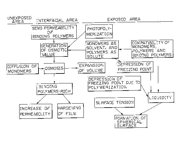
Figures 7 and 8 are diagrams showing a mechanism of
the formation of the lens according to the present
invention, by which the lens forming mechanism of the
present invention will be further clarified. In the
following description, if there is a mixture of two or
more substances, a substance having a relatively higher
evaporation pressure and smaller molecular size is
defined as a "solvent", and another substance having a
relatively lower evaporation pressure and larger mole-
cular size is defined as a "solute". Thus, in this
instance in which photopolymerizable substances are used
as the photoreactive compound, monomers act as a solvent,
and polymers, reacted products, act as a solute.
A comparison of the composition of the light-
lS sensitive film in the exposed area and the unexposed
area, as well as before, during, and after exposure, is
summarized in the following Table 1.
- 17 -
Table 1
UnexposedExposed
area area
_
Before M M
exposure
sP sP
(S) (S)
_
During M osmosis ~ M
exposure
BP HPD-P
(S) LPD-P
BP
(S)
After M M
exposure
HPD-P
BP BP
Before selective exposure, the light-sensitive film
contains photopolymerizable substances, monomers M,
binding polymers BP, and a solvent S (if necessary).
During exposure, the monomers M in the unexposed
area permeate or migrate into the exposed area, and in
the exposed area, as a result of photopolymerization
caused by the exposure, polymers with a low polymeriza-
tion degree (LPD-P) and polymers with a high polymeriza-
tion degree (HPD-P) are concurrently produced. This
stage will be further described with reference to
Fig. 8, showing an interfacial area 5 between the
exposed and unexposed areas of the light-sensitive
film 2. In the inter~acial area 5, the binding polymers
BP are rich and the monomers M are poor. Accordingly,
3~2~4~7~
- 18
and since the area 5 is harder than other portions of
the film 2, the area 5 acts as a "semipermeable mem-
brane". The monomers M diffuse in each of the exposed
and unexposed areas, and, as shown by the arrows M,
permeate from the unexposed area through the interfacial
area or semipermeable membrane to the exposed area due
to an osmotic pressure created between the two areas.
The dotted line in the unexposed area indicates that the
concentration of the monomers M is reduced by the amount
plotted. In the exposed area, polymerization of the
monomers M occurs, and thus the amount of the polymers
HPD-P, LPD-P, and B is gradually increased. However, in
spite of the increase of the polymers in the exposed
area, a liquidity or property as a liquid of the film
in this area is constantly maintained because of the
depression of the freezing point also created in this
area. In Fig. 7, while it is shown that the depression
of the freezing point is due to polymerization, the
freezing speed is also reduced due to polymerization is
some cases. Further, since a surface tension acts on a
surface of the liquid or liquid-like film, the roundness
which i5 essential to the formation of a lens is con-
ferred on the film surface.
After exposure, the binding polymers BP and a small
amount of the monomers M remain in the unexposed area.
On the other hand, polymers HPD-P, the monomers M, and
the binding polymers BP remain in the exposed area. The
monomers M, i.e., unreacted compounds, in this area can
be removed from the film by heat treatment or converted
to HPD-P polymers by an overall exposure.
During the photopolymerization, the monomers M and
the polymers LPD-P and HPD-P in the light-sensitive film
each act as follows:
Monomers M ............ diffusion in the exposed and
unexposed areas
-- 19 --
Polymers LPD-P ... diffusion in a mix~ure of the
monomers M and ~he solvent S
tif any)
The expansion of the volume in the exposed area of the
film is caused by osmosis and swelling, explained as
follows:
Osmosis .... The monomers M and the polymers LPD~P
each act as a solvent and as a solute.
Upon exposure, a concentration of the
solute is increased, and thus an
osmotic value is generated in the
interfacial area between the exposed
and unexposed areas, and accordingly,
the monomers M in the unexposed area
migrate into the exposed area.
Swelling ... The monomers M act as a solvent, and
the polymers HPD-P and the binding
polymers BP act as a solute. Before
exposure, the film is considered to in
a swelling condition in thermal
equilibrium. With the progress of the
exposure, the polymers HPD-P are
produced in the exposed area, and
therefore, thermal equilibrium in this
area is broken. To maintain thermal
equilibrium, the exposed area absorbs
the solvent, i.e. monomers M, from the
areas adjacent thereto, and as a
result, the exposed area is expanded.
The formation of a spherical surface of the film in
the exposed area is caused in particular by the lowering
of the freezing point and freezing speed and by the
surface tension. First, the following reaction is
induced when the light energy acts on the monomers M:
monomers M > monomers M ~ polymers LPD-P
Namely, a mixture of M and LPD-P is produced. Since
this reaction lowers the freezing point and freezing
~2~71[3
- 20 -
speed, a liquid state of the film is retained. Further,
due to this liquid state of the film, and for other
reasons, a surface tension is also induced in the film.
These phenomena cause the formation o~ a spherical
surface of the film.
The formation of the lens depends on various
factors such as the film thickness, composition and
concentration of the film, exposure conditions, and
specific materials used. To ascertain this phenomenon,
the lens was produced in accordance with the present
process and by using cinnamyl chloride as the photo-
reactive compound and polymethylmethacrylate (polymeri-
zation degree of about 10,000) as the binding polymer.
The following results were obtained.
Thickness of film:
The relationship between the thickness of the film
and the diameter of the lens is plotted in Fig. 9. This
data was obtained at an exposure time of 60 min. and a
cinnamyl chloride concentration of 67% by weight. From
this graph, it can be seen that the diameter of the lens
is increased in accordance with the increase of the film
thickness. This is because, if the film has a large
thickness, a much larger amount of the monomers can
migrate into the exposed area of the film.
Composition of film:
The relationship between the cinnamyl chloride
concentration and the diameter of the lens pattern is
plotted in Fig. 10. This graph indicates that, when the
lens is produced, a larger diameter is obtained if there
is a higher concentration of the monomers in the film.
The reason for this relationship is the same as that for
the relationship between the film thickness and the
diameter of lens discussed above. In addition, if the
concentration of the monomers in the film is increased,
the polymers, which are also included, can move more
easily in the film, and as a result, the diameter of the
lens is increased.
:~2~ 7~
- 21 -
Diameter of exposed area:
The configuration of the lens depends on the
diameter of the exposed area. Figures 9 and 10 indicate
that, assuming tha~ the thickness and composition of the
film are constant, a ring-shaped lens can be obtained
when the diameter of the exposed area is large, and a
lens with an excessively large diameter and having no
power to condense light can be obtained when the exposed
area has a small diameter.
Exposure conditions:
Figure 11 is a graph showing the relationship
between the exposure time and the focal length of the
lens. This graph shows that a shorter focal length is
obtained with a longer exposure time. In addition, a
shorter focal length can be also obtained by a higher
exposure intensity of the radiation. However, an
excessively high exposure intensity must be avoided,
since this will cause a hardening of the film in a
central portion of the exposed area, and the hardening
of the film in the exposed area will prevent the swelling
of the film. The exposure temperature is preferably
plus or minus 40C. A lower temperature than the above
will not allow a permeation of the monomers from the
unexposed area to the exposed area, and at a temperature
higher than the above lenses with an unacceptably large
diameter will be formed.
As is apparent from the above descriptions, accord-
ing to the present invention, it becomes possible to
produce micronized optical elements such as microlenses
and arrays thereof. The optical elements can be freely
designed. Further, because the resulting optical
elements are in the form of a film or coating, they can
be easily integrated with other optical elements.
Furthermore, because of the simple production process,
the optical elements can be produced on a mass-production
scale and with low production costs.
In the practice of the present invention, selective
~2~
- 22 -
exposure of the light-sensitive film is generall~
carried out through a photomask disposed on the film.
Alternatively, it is possible to carry out the selective
exposure through a photomask disposed between the
light-sensitive film and the underlying substrate. This
method is referred to herein as a back-side exposure and
will be explained hereinafter with reference to Figs. 12A
to 12C.
In Fig. 12A, a substrate 21 has a mask 23 of
chromium and chromium oxide deposited thereon. The
mask 23 acts a photomask and as a shadow mask, as
described below. Since the selective exposure is
carried out from the substrate side, the substrate 21
must allow the passage therethrough of the exposure
radiation. Therefore, preferably a glass substrate is
used as the substrate 21. A light-sensitive film 22
containing photoreactive compounds is coated over the
substrate 21.
The back-side exposure is conducted as shown in
20 Fig. 12B, to produce the lenses 24 of Fig. 12C. From
Fig. 12C, it is clear that the exposed area 24 has a
lens shape and the unexposed area 25 has a reduced films
thickness. The shadow mask may be formed from a part or
whole of the photomask. The resulting optical device
having a shadow mask incorporated therein can be effec-
tively used, for example, in the production of image
sensors.
Since the mask used herein as the photomask also
acts as a shadow mask and a back-side exposure is used,
drawbacks due to use of the usual shadow mask can be
prevented. For example, it is not necessary to align
the lens with the shadow mask, and therefore lenses are
not damaged during an alignment step, and a poor accuracy
of the lens due to a reflection of the exposure light
from the back surface of the substrate is avolded.
Figure 13 is a modification of the optical device
of Fig. 12C. The device illustrated in Fig. 13 has a
~2~
spacer 26 provided between the lens-retaining film 26
and the shadow mask 23. The spacer 26 is used to obtain
a planar surface to which the light-sensitive film is
applied.
Figures 14A to 14C illustrate, in sequence, the
production of concave microlenses according to another
embodiment of the present invention. The lens production
mechanism in the illustrated instances is substantially
the same as that used in ~he production of the convex
lenses described above~
First, as shown in Fig. 14A, a light-sensitive
film 32 containing photoreactive compounds such as
monomers is coated on a substrate 31. Then, as shown in
Fig. 14B, the light-sensitive film 32 is exposed to
radiation passed through windows 34 of the photomask 33,
to cause a variation in the configuration of the film 32.
After exposure, concave lenses 35 are formed in the
film 32 (see Fig. 14C), and finally, the unreacted
photoreactive compound in the film 32 is stabilized as
2~ previously described.
The formation of the concave microlenses and arrays
thereof will be further described with respect to the
preferred embodiments shown in Figs. l5A and 15B and
Figs. 16A and 16B.
Figure 15A illustrates a photomask 33 with ring-
shaped windows 34. The position of the windows 34 in
the mask 33 corresponds to that of the lenses 35 to be
formed on the light-sensitive film 32 (see Fig. 15B).
During the exposure step, the exposure radiation passed
3~ through the windows 34 of the mask 33 will irradiate
only limited areas, namely, peripheral portions of the
lens-providing area of the film 32. As a result, in the
film 32, the monomers in the light-irradiated areas are
polymerized to dimers or other polymers, thereby obtain-
ing a mixed composition of the monomers and dimers orpolymers. Since the mixture in the exposed areas has a
lower evaporation pressure than that of the monomers in
- 2~ -
the unexposed areas, the monomers in the unexposed areas
are absorbed by and migrated into the exposed areas, and
the exposed areas thus expanded. In this instance,
since the exposed areas are in the form of a ring, the
monomers are absorbed from the inner and outer unexposed
areas adjacent to the ring-shaped exposed area. With
the expansion or raising of the ring-shaped exposed
area, a central portion of the exposed area relatively
subsides, and finally, as shown in Fig. 15B, concave
lenses 35 with a small curvature are obtained.
Figures 16A and 16B illustrate another example of
the production of the concave microlenses and arrays
thereof according to the present invention. As showII in
Fig. 16A, a photomask 33 has a plurality of square
windows 34 which are disposed in a grid pattern. After
a selective exposure using the photomask 33, a plurality
of concave microlenses 35 are formed in the unexposed
area of the light-sensitive film 32. The resulting
microlens arrays can be used, for example, in fiber
optic communications.
According to another embodiment of the present
invention, a solvent is added to a film-providing
composition for use in the formation of the light-
sensitive film. The added solvent is then removed from
the film at the same time as or after the selective
exposure. This is particularly effective when satisfying
the following requirements:
(1) The photoreactive compounds must diffuse
within the light-sensitive film, and
(2) At least a mixture of the photoreactive
compounds and the reaction products thereof must be in a
liquid state, which conditions, as discussed above, are
essential in the mechanism of the formation of the
optical elements according to the present invention.
For example, photoreactive compounds or monomers
such as cinnamic acid or cinnamic acid cholesterol, if
used alone, can not diffuse within the light-sensitive
film. Also, a mixture of these monomers and the dimers
thereof is not usable, since such a mixture is solid at
a temperature at which the exposure radiations are
irradiated onto the film. Further, polymeric materials
with a high polymerization degree are not usable as the
binding polymers, since if the film contains such high
polymeric materials, the photoreactive compounds can not
diffuse in the film.
The above drawbacks are avoided by adding specific
solvents to the light-sensitive film, and as a result,
it can be ensured that the photoreactive compounds
diffuse in the film and the mixture of these compounds
and reaction products thereof has liquid properties.
The present inventors found that the combinations
lS of the photoreactive compounds, binding polymers and
solvents summarized in the following Table 2 are prefer-
able in the practice of the present invention, for
example:
Table 2
film- photoreactive binding solvent
providing compound polymer
composition
A cinnamic acid PMMA* 1,4-dioxane
B cinnamic acid PMMA* 1,4-dioxane,
cholesterol propylene carbonate
C cinnamic acid, PMMA* vinyl cinnamate
vinyl cinnamate
PMMA* polymethyl methacrylate
In the film-providing compositions A and B,
1,4-dioxane and/or propylene carbonate is used as the
solvent. After selective exposure, the solvent can be
removed from the film by annealing. In the ~ilm-
providing composition C, vinyl cinnamate is used as the
~æ~
- 26 -
solvent and as the photoreactive compound in combination
with cinnamic acid. Since vinyl cinnamate is a dimeriz-
able compound, after selective exposure of the film, it
can be stabilized by annealiny to cause a thermal
polymerization.
According to the present invention, it becomes
possible to use photoreactive compounds and binding
polymers, which can not used alone, as the light-
~ sensitive film-providing compounds in the production of
optical elements such as lenses and gradient thickness
films according to the present invention. Preferable
solvents include 1,4-dioxane and other solvents having
an evaporation pressure lower than that of 1,4-dioxane
at an exposure temperature.
According to another embodiment of the present
invention, after selective exposure of the light-
sensitive film, the exposed film is left to stand
without further irradiation of light to further vary a
configuration of the film. After this variation-
increasing step, the film is preferably subjected to
overall exposure to stop any further variation of the
film configuration. Penetration of the monomers as the
photoreactive compounds from the unexposed area to the
exposed area, and a corresponding increase of the film
thickness of the exposed area during this step, will be
stopped, since the remaining monomers are photopoly-
merized to become dimers and other polymers upon overall
exposure. A greatly increased thickness of the exposed
film will produce various optical devices having
excellent characteristics.
The above embodiment of the present invention can
be performed as follows. A light-sensitive film
containing at least photoreactive compounds is coated on
a substrate. The light-sensitive film used herein has
different compositions. For example, (1) it consists of
photoreactive compounds only, (2) it consists of the
photoreactive compounds and the binding polymers, (3) it
3 Z~gL7~
- 27 -
consists of the photoreactive compounds and the solvents,
or (4) it consists of the photoreactive compounds, the
binding polymers and the solvents. These photoreactive
compounds, binding polymers, and solvents have been
previously exemplified.
After formation of the light-sensitive film, the
film is subjected to selective exposure using a photomask
with windows. The pattern of the windows depends on
particular optical elements. Upon exposure, the evapora-
tion pressure of the photoreactive compounds in theexposed area of the film is varied as a result of
dimerization, isomerization, polymerization, and other
photoreactions. For example, when cinnamyl chloride is
used as the photoreactive compound and PMMA as the
binding polymer, cinnamyl chloride in the exposed area
of the film is dimerized by the irradiation of light,
and thus a remarkable reduction of the evaporation
pressure in the exposed area is obtained. Accordingly,
there is a coexistence of cinnamyl chloride monomers and
the dimers thereof in the exposed area. Under this
condition, unreacted cinnamyl chloride in the unexposed
area is continually absorbed by and moved to the exposed
area. On the other hand, cinnamyl chloride existing in
the exposed area remains there. Therefore, when the
exposed film is left to stand without a further irradi-
ation of radiation, a continuous supply of the unreacted
cinnamyl chloride in the unexposed area to the exposed
area occurs, and during that stage, the expansion of the
exposed area continues. A remarkably large variation in
the film thickness in the exposed and unexposed areas i5
thus obtained.
Figure 17 is a graph showing the relationship
between the exposure time and the variation of the
thickness of the light-sensitive film during the selec-
tive exposure step of the film. When the exposure iscontinued as shown by the dotted line A, the thickness
of the exposed film is gradually increased in accordance
~299~7~
28 -
with the exposure time. Further, although the rate of
increase of the film thickness is not higher than that
shown by line A, similar tendencies can be seen in the
solid lines B, C, and D. In the case of line B, the
exposure was interrupted at tl , line C at t2 ~ and
line D at t3 , respectively. After interruption of
the exposure, the exposed films were left to stand. The
graph of Fig. 17 indicates that, after completion of the
exposure, the increase of the thickness of the film in
the exposed area is not stopped, but is continued, even
if the film is not subjected to additional exposure.
When a desired distribution of the thickness of the
film is attained, the increase of the film thickness can
be stopped by overall exposure or annealing of the film.
All of the unreacted compounds are therefore optically
or thermally reacted to form the corresponding stable
reaction products, or are removed.
In accordance with still another embodiment of the
present invention, optical elements such as lenses and
` gradient thickness films can be produced by selectively
exposing a light-sensitive film containing at least
photoreactive compounds to exposure radiation, generating
differences in the concentration of the reaction produc~s
in the photoreactive compounds between the exposed and
unexposed areas of the film, and then causing, in an
interface between the exposed and unexposed areas, an
osmosis phenomenon causes a reduction in the differences
in the concentration, thereby varying the configuration
of the film.
The mechanism of this production process is illus-
trated in Fig. 18A (during exposure) and FigO 18B (after
exposure). In Fig. 18A, a substrate 41 is coated with a
light-sensitive film 42. The film 42 consists of
photoreactive compounds, particularly photopolymerizable
materials M and binding polymers BP. The photoreactive
compounds M are selected from those which can diffuse in
the film 42 and which when mixed with the reaction
~2~ 7~3
- 29 -
products thereof formed upon irradiation of radiation is
a liquid during exposure. The binding polymers BP are
selected from among those which can effectively generate
an osmosis or similar phenomenon in an interface ~4 of
the exposed area 45 and the unexposed area 46.
Selective exposure of the light-sensitive film 42
is conducted with radiation passed through windows of a
photomask 43. As a result, in the exposed area 45 of
the film 42, the reaction products P are produced from
the photoreactive compounds M. The formation of the
reaction products P is continued until the photoreactive
compounds M and completely consumed in the exposed
area 45, and therefore, the volume of the area 45 is
gradually increased. The smaller the ratio of the
exposed area 45 to the unexposed area 46, the larger the
volume of the area 45, and thus a difference in the
film thickness between the exposed and unexposed areas
is obtained.
The above action and mechanism will be further
described with reference to Figs. 18B and 19. The
action of the present process is substantially the same
as the osmosis phenomenon which, as shown in Fig. 19, is
generated when a solvent and a solute is separated with
a semi-permeable membrane 47. Namely, in the present
process, the photoreactive compounds M act as a solvent
and the reaction products P of the compounds M act as a
solute. The reaction products P are produced based on a
chemical reaction induced by an irradiation of radiation.
The interface 44 between the exposed and unexposed areas
acts as a semi-permeable membrane.
In Fig. 18B, the exposed area 45 of the film 42
contains the reaction products P in addition to the
reactive compounds M. When the reactive compounds M
have a solvent-like property with regard to the reaction
products P, a concentration of the reaction products P
in the exposed area 45 is increased upon the irradiation
of radiation, and with increase of the concentration, an
. .
- 30 -
osmosis phenomenon is generated which reduces the
concentration of the products P in the interface 44
between the exposed area 45 and the unexposed area 46.
The osmosis phenomenon then induces a migration of the
reactive compounds M in the unexposed area 46 into the
exposed area 4. As a result of the migration of the
compounds M, as indicated by "h", a large difference in
the film thickness is produced between the exposed
area 45 and the unexposed area 46.
According to this embodiment of the present inven-
tion, due to the osmosis phenomenon caused by the
irradiation of radiation, a notably large variation in
the thickness of the light-sensitive film can be attained.
Further, assuming that an outer force such as gravity
does not act upon the system, an expansion of the volume
of the film will be continued until the photoreactive
compounds in the film are exhausted. Such a large
variation in the configuration of the film is practically
very useful in the production of the optical elements.
In accordance with still another embodiment of the
present invention, optical elements such as lenses and
gradient thickness films can be produced by selectively
exposing a light-sensitive film containing at least
photoreactive compounds to form reaction products of the
photoreactive compounds, and swelling the reaction
products by the absorption of certain compounds which
are also contained in the film, thereby varying the
configuration of the film.
The formation of the optical elements in this
embodiment relies upon a swelling of the reaction
products in the exposed area of the light-sensitive
film~ The reaction products are swollen, because they
can absorb certain compounds which are also contained in
the film. Although the compounds to be absorbed by the
reaction products are not restricted, insofar as they
are compatible with other compounds in the film and are
absorbed by the reaction products, such compounds are
~Z~7~
.
- 31 -
preferably identical wi-~h the photoreactive compounds
used. The present inventors found that a photopolyme-
rizable compound such as cinnamyl chloride is effective
for this purpose.
The above-described formation of the optical
elements will be further described with reference to
Figs. 20A and 20B. A light-sensitive film 52 is
positioned on the substrate 51 and consists of photo-
reactive compounds M, compounds N capable of being
absorbed by the reaction products P of the compounds M
(compounds N may be the same or different from the
compounds M), and binding polymers BPo As the photo-
reactive compounds M, any compounds which are diffusible
in the film 52 and the reaction products P thereof
produced by the irradiation of radiation can swell as a
result of an absorption of the compounds M and/or N, can
be used. For example, suitable photoreactive compounds M
include cinnamyl chloride, and suitable compounds N
include a mixture of cinnamyl chloride and 1,4-dioxane
as a solvent or methylmethacrylate oligomers.
As illustrated in Fig. 20A selective exposure of
the film 52 is carried out through a photomask 53.
During this exposure, reaction products P of the com-
pounds M are produced in the exposed area 55. These
reaction products P absorb the compounds M and/or N
contained in the exposed area and swell. Then, the
absorbed compounds M further produce reaction products P.
These new reaction products P absorb the compounds M
and/or N diffused from the unexposed area 56 and swell~
The exposed area 55 containing the reaction products P
therefore continues to swell, so long as the compounds M
and/or N are supplied to that area. Figure 20B shows
the results of the formation process according ~o the
described embodiment.
According to the present invention, a large varia-
tion in the form of the light-sensitive film can be
obtained because the expansion of the exposed area of
- 32 ~
the film is induced by the irradiation of radiation.
Further, if an outer force such as gravity does not
affect the system, the expansion of the exposed area
will be continued until the photoreactive compounds in
the film are exhausted. Accordinglv, optical elements
such as gradient thickness films having a remarkably
varied film form can be obtained.