Note: Descriptions are shown in the official language in which they were submitted.
~2~ 5
PHD 85097 l 20,5.1986
Circuit arrangement ~or operating high-pressure gas
discharge lamps.
The invention relates to a circuit arrangement
for operating at least one high-pressure gas discharge lamp
at current of higher frequency, which comprises a full-wave
rectifier to beconnected to an alternating voltage source
and having direct voltage output terminals connected to a
first circuit part comprising a switching transistor9 a
choke coil, a fly-wheel diode and a storage capacitor for
feeding the lamp The duty cycle and/or the switching
frequency of the switching transistor are controlled by a
10 control device in such a manner that the current load of
the alternating voltage source is as sinusoidal as
possible.
The term "current of higher frequency" is to
be understood herein to mean a current of a periodically
15 varying value having a frequency between 1 kHz and 500kHz
and preferably between 20 kHz and 150 kHz.
Such a circuit arrangement comprising, ~or
example, a boost or up converter as the first circuit part
is known from EP OS 0059053~ In general, storage capacitors
20 0~ comparatively high capacitance are used, for example,
220/uF/I~OO ~ with a power consumption o~ the lamp of 130 W.
In order to guaran-tee a minimurn life of the storage
capacitors, a comparatively large number of electrolytic
capacitors is required. Otherwise, the capacitors would be
25 heated excessivaly due to the high-frequency current pulses.
Therefore, it would be desirable to use foil capacitors
for the storage capacitors. In the known circui-t arrange-
ments, however, this solution would have the disadvantage
that due to their low storage capacity per unit volume no
constant direct vol-tage, but a direc-t voltage pulsating at
double the mains frequency occurs at the storage capacitor~
However~ only a small direct voltage fluctuation is often
PHD 85097 2 2055,1986
desirableO The control for a usually employed boost or
up converter is very simple if a constant output direct
voltage is presupposed. On the other hand, not too large a
voltage fluctuation is also favourable for the behaviour
of high-pressure gas discharge lamps because these lamps
extinguish at voltages below their operating vol-tage.
A reignition of high-pressure gas discharge lamps is only
possible, however, if shortly after the lamp has
extinguished again a suf-ficient voltage (re-ignition
voltage) is available at the storage capacitor.
Therefore, the invention has for its object
to provide a circuit arrangement for operating at least
one high-pressure gas discharge lamp in which on the one
hand a source load as sinusoidal as possible is obtained
with low inherent losses and on the other hand a smallest
possible storage capacitor is sufficient with a small
voltage fluctuation at this storage capacitor.
According to the invention, in a circuit
arrangement of the kind mentioned in the opening paragraph
this object is achieved in that a second circuit part
comprising at least one electronic switching element is
arranged between the storage capacitor and the lamp and can
be controlled by a control device upon comparison of an
actual-value signal proportional to the instantaneous lamp
current of higher frequency with a nominal-value signal
consisting of a sinusoidal voltage having double the
alternating voltage source frequency and of a d,c.
voltage component having a value of at least the maximum
amplitude of the sinusoidal voltage.
Such a circuit arrangement produces a lamp
current, which modulates a high-frequency component which
depends upon the switching frequency of the electronic
switching element and whose frequency usually lies between
1 and 500 kHz and preferably between 20 and 1So kHz. The
lamp current pulsates at the rhythm of double the so-urce
frequency, to which a d.c. component is added. Th~
~; required nominal-value signal part sin2 ~ t is then
s
PHD 85097 3 20.5.1986
preferably formed from the voltage ¦sin ~ t ¦
which is present behind the full-wave rectifier and in
whose Fourier development as a 1 harmonic the function
cos ~ t is contained. According to the formula sin ~ t =
~ cos ~ t)~ the square of the sine can be formed
therefrom by superimposir&~on it a d.c. component.
The term "circuit part" is to be understood
herein to m0an any type of converter, such as, for example,
a buck or down conve~er, a boost or up converter, a buck-
boost converter, a fly-back converter~ a forward converter
a push-pull converter, a bridge converter etc. In an
advantageous further embodiment of the circuit
arrangement according to the invention, an opto-
coupler is connected to the full -wave rectifier for forming
the nominal-value signal from the rectified source voltage
through an RC combination~
In another advantageous embodiment according
to the invention, the second combinatorial circuit part
is a buck or down converter, and the nomina~value signal
20 is being formed from a voltage drop at the el~ctronic
switching element through an RC combination~
In order that the invention may be readily
carried out, it will now be described more fully3 by
way of example, with reference to the accompanying drawing,
25 in which:
Fig. 1 shows a circuit arrangement for operating
at least one high-pressure gas discharge lamp comprising
an up converter~ which is controlled through a control
device and which is sùcceeded by a down converter contr~lled
30 through a control device.
Fig. 2 shows the circuit diagram of the control
; dcvice used in the circuit arrangement shown in Fig~ 1,
Fig~ 3 shows the circuit diagram of another
control device.
Fig. 4 shows the voltage varia-tion at the
output ofthe full-wave rectifier of the circuit arrangement
shown in Fig. 1,
~ig. 5 shows the variation of the nominal-
~2~6~;
PHD 85097 ~ 20.5 1~86
~alue signal in the circuit arrangements shown in
Figures 2 and 3,
Fig. 6 shows the current variation through
the lamp.
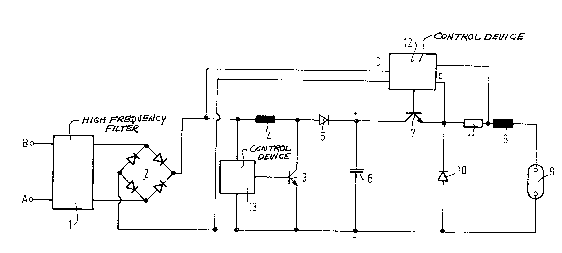
In Fig. 1, A and B designate input terminals
for connection to a mains of, for example, 220 V, 50 Hz
serving as an alternating voltage source. A full-wave
rectifier 2 comprising four diodes is connected to these
output terminals A and B throu~h a high-frequency filter 1.
An up converter comprising a switching transistor 3, a
choke coil ~, a fly-wheel diode 5 and a storage capacitor
6 and serving as the first combinatorial circuit part is
connected to the output direct voltage terminals of the
full-wave rectifier 2. A direct voltage of at most 400 V
is applied to the storage capacitor 6, which has a
comparatively small capacitance of, for example~ 1.5/uF.
A down converter serving as the second circuit
part and comprising an electric switching element 7 in the
form of a second switching transistor, a choke coil 8 and a
fly-wheel diode 10 is connected parallel to this storaæe
capacitor 6. A connected lamp 9 is shown at the down
converter. The lamp circuit further includes a measuring
resistor 11 which sets as a current sensor and at which an
actual-value signal is derived, which is proportional to
the instantaneous lamp current and which is fed to the
input C of a control device 12~ The lamp current I is
tracked through the control device 12 in the mannar to be
descnbed below by a nominal-value signal derived from the
recti~ied mains voltage applied to the input D of the
control device 12.
A control device 13 for controlling the duty
cycle and/or the switching frequency of the switching
transistor 3 operates in such a manner that the current
taken up from the alternating voltage mains varies as
sinusoidally as pos~ible. Such control devices are known
se, for example, from DE OS 2~52275.
The control device 12 serves to keep the
3~6.~
PHD 85097 5 20.5.1986
~oltage fluctuation at the storage capacitor 6 as small
as possible. An embodiment of such a con-trol de~ice 12
will now be described more fully with reference to
Fig. 2. A sinusoidal voltage having double the mains
frequency is formed frorn the voltage U0 = ¦ sin ~ t¦
(Figo 4) applied to the direct voltage output terminals of
the full-wave rectifier 2 through a resistor 14, an opto-
co pler 15 and a variable resistor 16 at a capacitor 17
connected parallel to the latter resistor. An RC
combination comprisin~ a variable resistor 18 ancl a
capacitor 19 serves to cause the phase of the nominal-
value signal, which is last applied to the inputs of the
comparators 20 and 21~ to correspond to the phase of the
mains voltage, A capacitor 22 serves to cut off the d.c.
component, which can be arbitrarily adjusted by means of
a variable resistor 23. Thus, it can be achieved that a
nominal-value signal Us ll = a sin2 ~ t ~ b can be supplied
to the inputs of the comparators 20 and 21 (Fig. 5),
The constant b may of course also become zero~ The
nominal-value signal U ll consists of a sinusoidal signal
having d~uble the mains frequency and a d.c. component
having a value of at least the maximum amplitude a/2 of
the sinusoidal signal. In Fig. 5, the d.c. component is
indicated by the broken line x-x.
Through a variable resistor 24, an upper
limit level can be adjusted at the comparator 20~
Through resistors 25 and 26, a lower limit level can
be adjusted at the comparator 21. Capacitors 33 and 34
serve to suppress high-frequency interference signals. The
actual value signal proportional to the lamp current and
derived at the measuring resistor 11 is divided through a
capacitor 27 and a potentiometer 28 and is supp~ed to
the comparators 20 and 21. The output signals of the
comparators 20 and 21 are supplied to the reset input R
and to the set input S, respectively, of a bistable
trigger circuit 29. The signal a-t the output F of the bi-
stable trigger circuit 29 now switches the transistor 7 to
PHD ~5097 ~ 20~5.1986
the conducting state and to the non-conducting state,
respectively.
A stab-~ized direct voltage of, for example,
12 V applied to the point G can adjust the system
automatically and is used for the voltage supply of the
electronic system and is supplied through resistors 30
and 31 to the outpu-ts of the comparators 20 and 21.
The control device 12 then operates in such
a manner that, when an upper nominal-value level UsOll
is reached, the switching transistor 7 is switched to the
non-conducting state; when a lower nominal-value level uU ~L
is reached, the transistor 7 is switched again to the
conducting state (Fig, 6). The switching frequency of
the switching transistor 7 varies during the 100 l~z
periods, but preferably lies between 20 and 150 kHz, in
accordance with the size of the choke coil 8, Fig. 6
shows the variation of the lamp current I, which
mainly corresponds to the variation of the nominal-value
signal shown in Fig. 5, on which the switding frequency
of the switching transistor 7 is superimposed.
During operation of a 50 W mercury high-pres-
sure lamp, it can be achieved with this embodiment that
the voltage fluctuation at the storage capacitor 6 is
smaller than 60 V~ This at the same time leads to a
purely sinusoidal mains current. However, when, as known,
a constant direct voltage is chosen as the actual-value
level, a voltage fluctuation of substantially 400 V is
obtained, which leads with the same up convertor to
considerable mains distortions. In order to avoid this,
in this kind of control, a considerably larger capacitor 6
should be used (about 10/uF) J
The control device 12 shown in Fig~ 3 mainly
corresponds to the device shown in Fig. 2. However,
instead of using the opto-coupler, the nominal-value
signal is formed from a vol-tage drop at the switching
transis~r 7 in that a voltage is derived across the
switching transistor 7 and the measuring resistor 11 and
6~5
PHD 85097 7 20.5~1g86
this voltage is supplied to the variable resistor 16 via
a resistor 32.
In a practical embodiment comprising a
control device as shown in ~ig. 2 for operating a
50 W high-pressure mercury lamp having a lamp operating
voltage of about 90 V a-t a mains alter~ting voltage of
220 V, 50 Hz, and a voltage at the storage capacitor 6
of at most 400 W, the following circuit e]ements were
used:
: 25
; 35
PHD 85097 8 20.5.1986
Resistor 11 1 Ohm
Resistor 14100 kOhm
Resistor 1647 kOhm
Resistor 1822 kOhm
Resistor 231 MOhm
Resistor 24 4.7 kOhm
Resistor 25 4.7 kOhm
Resis-tor 26 4.7 kOhm
Resistor 281 kOhm
Resistor 3033 kOhm
Resistor 3133 kOhm
Capacitor 61,5/uF 400 V
Capacitor 17100 nF
Capacitor 19100 nF
Capacitor 22220 nF
Capacitor 2733 nF
Capacitor 3310 nF
Capacitor 3410 nF
Choke coil 4 1 mH
Choke coil 8 1 mH
Diode 5BY 229 Valvo
Diode 10DSR 5500x TRW
Opto coupler 15CNY 62
Comparators 20~ 21 2x 1/4 LM339 ) Val~o
bistable trigger circuit 29 HEF 4027