Note: Descriptions are shown in the official language in which they were submitted.
7~
DOUBLE-SWITCHED PLYBACK POWER-CONVERTER
This invention relates generally to power converters
and, more particularly, to double-switched flyback
converters.
Modern electronic sys.ems require power regulation to
condition the output of the primary power source. Power
converters provide a regulated DC voltage from a primary
DC source. Conventional DC/DC converters are ger.erally of
~ the push-~ull or switching regulator type.
:; '
A ~lyback converter uses a switching regulator to
cyclically store and transfer energy from a primary DC
source through a pc~er transformer to an output circult.
The prlmary winding of the power transformer is connected
to the primary DC source: the secondary winding is
connected to the output circuit. The switching regula~or
alternately opens and closes a switch connecting the
pr mary DC source to the primary winding of the-
transformer. This switching action defines a power cycle
which inductively couples 'he primary 3C source to the
output circuit.
'
: :~
7~
--2--
The power cycle of the converter comprises two parts:
a primary conduction cycle and a flyback cycle. During
the primary conduction cycle, the switch is closed,
transferring energy from the primary DC source to the
primary winding of the power transformer. At a preset
power level in the primary winding, the switch is opened,
starting the flyback cycle. During this cycle, energy is
coupled through the secondary winding into a rectified
output circuit.
The amount of energy stored per cycle is controlled
by regulating the s-~itching action. Generally speaking, a
pulse width modulating (PWM) circuit regulates the
switching action by varying the pulse width or "on" time
of the switches. Negative feedback of the output voltage
is frequently used in conjunction with the PWM circuit to
provide output voltage regulation.
A double-switched flyback converter uses two switches
in series and on opposite ends of the primary winding of
the transformer. The switches, typically, are high
voltage transistors driven by a gate drive transformer
connected directly to the PWM circuit. The PWM circuit,
acting through the gate drive transformer, biases the
gates of the transistor switches to the "on" state,
storing energy in the primary winding during the primary
conduction cycle. The gates of the transistor switches
are subsequently biased to the "off" state during the
flyback cycle.
In known converters, transien~s ln the primary DC
source or output load may impose undesirable str-esses in
the converter circuit. For instance, a surge in the input
voltage may transfer excess energy to the primary winding
during the primary conduction cycle; during the subsequen~
flyback cycle, the PWM circuit may command the transistor
~46~7~
--3--
switches "on" before the energy transfer to the secondary
winding is complete. This condition imposes high stress
currents on both the transistor switches and the power
transformer, leading to possible component failure. This
condition occurs because the PWM circuit is blind to the
exact status of the energy transfer at the power
transformer. Therefore, it is desirable to monitor the
status of the energy transfer at the transformer windings
to provide for more efficient swi-tching action.
The invention overcomes the above-noted and other
drawbacks of the prior art by providing a method and
apparatus using a double-switched flyback power-converter
that features the capability of monitoring the exact
status of the energy transfer at the power transformer
windings. This capability allows for more efficient
switching in the power cycle and obviates the need for the
PWM circuit to control the switching action.
The invention in one aspect provides a regulated DC
power supply comprising means for receiving an AC voltage
input, rectifying means for developing a DC voltage from
the AC voltage input, a power transformer having a primary
winding and a plurality of secondary windings, and a
switch means coupled in series with the rectifying means
and the transformer. A sensing means senses the current
in the primary winding of the transformer, and a first
control means is responsive to the sensing means for
opening the switch means at a first predetermined current
in the primary winding of the transformer. A second
control means is powered :Erom a first secondary winding
for closing the switch at a second predetermined current
in the primary winding of the transformer, and output
means is coupled to a second secondary winding for
coupling the second secondary winding to a load.
The invention in another aspect provides a method of
converting a first DC voltage level to a second DC voltage
,,~.-,i
67~
level, comprising the steps of providing the first DC
voltage level to the primary of a flyback transformer,
commencing a primary conduction cycle by shutting a switch
in series with the primary winding, storing energy in the
primary winding of the transformer during the primary
conduction cycle, sensing the current in the primary
winding of the transformer and, at a predetermined current
level commencing a flyback cycle, during which energy is
transferred to secondary windings of the transformer,
depleting most of the energy in the secondary windings in
a load secondary winding and applying the remaining
portion of the energy in the secondary winding to a charge
pump circuit, the charge pump circuit controlling the
shutting of the switch in series with the primary winding,
and when the energy stored in the primary winding is
substantially depleted, shutting the switch to commence
another primary conduction cycle.
More particularly, the double-switched flyback power-
converter has a transformer primary winding connected
between the output terminals of a high voltage DC power
supply. A first switch is connected between the positive
terminal of the power supply and a first end of the
; primary winding. A second switch is ccnnected between the
negative terminal of the power supply and a second end of
the primary winding. A power output circuit is connected
to one of three secondary windings and a charge pumping
circuit is connected to each of the other two secondary
windings.
During the primary conduction cycle, a current
sensing means monitors the primary winding current and
signals a control logic circuit at a predetermined current
level. The control logic circuit then turns off the
second switch, forcing the power transformer into the
flyback mode of operation.
,: ~
~2~
--4--
During the flyback cycle, energy stored in the
primary winding of the power transformer is coupled to the
secondary windings. A major portion of the energy s
transferred to the power output circuit where it i,
rectified and filtered for output use. The remainder of
the energy is transferred to the charge pumping circuit at
each switch.
When the stored energy in the primary winding is
depleted, the charge pumping circuit pumps the charge
stored from the flyback cycle into the switches. The
switches turn on, returning the double-switched flyback
power converter to the primary conduction cycle. The
total power cycle is now complete and .eady to repeat.
The above-noted and other aspects of the present
invention will become more apparent from a description of
the preerred embodiment when read in conjuncrion with the
accompanying drawings.
The drawings illustrate the preferred embodiment of
the invention, wherein like members bear like reference
numerals and wherein:
Fig.l illustrates a double-switched flyback power-
converter in a block diagram form;
Fig.2 illustrates a circuit diagram of the double-
switched flyback power-converter used in the preferred
embodiment of the disclosed invention;
Fig.3 illustrates a waveform diagram of the circuit
;~ diagram illustrated in Fig.2;
5--
Fig.4 illustrates an alternative rectifier and filter
circuit enabling the double-switc~ed flyback power
converter to operate from different line voltages.
Fig.5 depicts a known, double-switched flyback
power-converter.
Fig.5 depicts a known flyback power-regulator 10. A
PWM circuit 200 provides duty cycle switcning to a gate-
drive transformer T21. An error amp input feedback line
202 indicates to the PWM circuit variation of the voltage
out of the power-regulator 10 from a reference (not
shown). Current through a primary winding 204 of the
gate-drive transformer T21 creates a flux that is coupled
to a pair of secondary windings 206 and 208. Flux
reversal at the secondary windings 206 and 208 drives the
gates of a pair of switches represented by transistors Qll
and Q21. When transistors Qll and Q21 conduct, flux
builds up in a primary winding 210 of a transformer Tll.
A subsequent pulse to the gate-drive transformer T21 opens
the switches Qll and Q21 to initiate the flyback cycle at
the transformer Tll. A diode CR31 rectifies the voltage
developed at the secondary 212 of the transformer Tll,
which voltage is filtered by capacitor Cll. A resistor RL
represents the load. A current sense resistor Rll
provides a signal to the PWM circuit indicative of the
primary current at transformer Tll. Line 202 and Rll
indicate to the PWM 200 :~hen to end a primary conduction
cycle and allow stored energy to be transferred to the
secondary ~iinding 212.
~ ig. 1 depicts a double-s~itched flyback po~er-
converter 20 in block diagram form. A 110 VAC line 22
prov~des input po-~er to a rectifier and filter circuit 24.
The rectifier and filter circuit 24 provides a high
6~
--6--
voltage 3C supply to the double-switched flyback power-
converter 20.
A conductor 26 connects the positive side of the high
S voltage DC supply to one side of a first high-voltage
switch ~8. A second high-voltage switch 32 connects to
the negative side of the high voltage DC supply through a
conductor 33. The primary winding of a power transformer
30 connects in series between the first high voltage
switch 28 and the second high voltage switch 32.
During the primary conduction cycle, the power
transformer 30 receives current through the high-voltage
switches 28 and 32. A current monitor 34 measures the
current passing through the high voltage switches 32 and
28 and the primary winding of the transformer 30. The
current monitor c~nverts the current to a voltage level
and sends the voltage level to the control logic circuit
36. The control logic circuit 36 ends the primary
conduction cycle by turning off the second high voltage
switch 32, beginning a flyback or a power conversion
cycle. Energy stored in the power transformer 30 during
the primary conduction cycle is depleted during the
flyback cycle by current generated in the secondary
windings of the power transformer 30. A power output
rectifier and filter circuit 3~3 connected to o-e of the
secondary windings rectifies and filters a major portion
of the secondary current.
:
Upon transformer flux depletion during the flyback
conversion cycle, current stops flow ng in the secondary
windings. ~lux depletion allows the double-swit-ched
flyback power converter to begin the primary conduction
cycle. This characteristic overcomes the dangers of
making connection to a charged inductive circuit with the
corresponding risk to semiconductor components.
~::
~2`~ 7~L
--7--
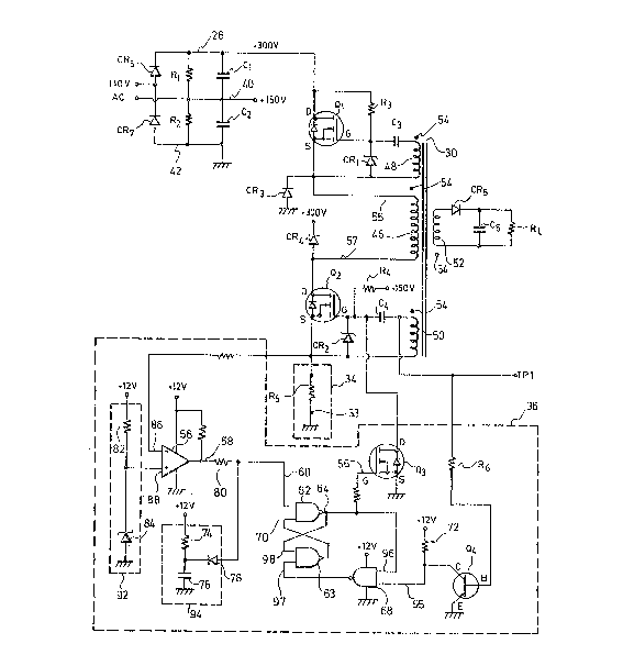
Fig.2 provides a more detailed depiction of the
double-switched flyback power-converter 20. A pair of
diodes, CR6 and CR7, rectify the 110 VAC line voltage.
Current flows through rectifier diode CR6 during the
positive half of the input cycle, charging a smoothinq
capacitor Cl to approximately 150 V. Current flows
through rectifier diode CR7 during the negative half of
the input cycle, charging a smoothing capacitor C2 to
approximately 150 V. The negative side of capacitor C2 is
grounded; the positive side of the capacitor C2 connects
to a conductor 40 and remains at approximately 150 V. The
negative side of the capacitor Cl connects to the
conduc-or 40; the positive side of capacitor Cl connects
to conductor 26 and is approximately 300 V above ground.
Resistors Rl and R2 bleed current from capacitors Cl and
C2 respectively.
The power transformer 30 includes a primary winding
46, a first secondary winding 48, a second secondary
winding 50, and a third secondary winding 52. A dot 54 at
one end of each winding shows the polarization of the
windings. For consistency, the end of a winding having a
dot will be referred to as the first end of the winding,
and the opposite end of the winding will be referred to as
the second end of the winding. A first end 55 of the
primary winding 46 is connected to the 300 V supply via an
enhancement mode MOSFET transistor Ql. A second end 57 of
the primary winding 46 is connected to ground via a second
enhancement mode MOSFET transistor Q2 and a resistor ~5.
Transistors Ql and Q2 are the high voltage switches 28 and
32, respectively, of r i9.1.
A first end of the first secondary winding 48
connects to a capacitor C3. A second end of the first
secondary winding connects to the source S of transistor
Ql. Current from the 300 VDC supp~y flows through a
8--
resistor R3 to initially charge the gate of transi_tor Ql.
Thereafter, the gate of Ql is controlled by a circuit
comprising the first secondary winding 48, the capacitor
C3 and a zener diode CRl.
A first end of the second secondary winding 50
connects to a capacitor C4. A second end of the second
secondary winding connects to the source S of transistor
Q2. Current from the 150 VDC supply flows through a
resistor R4 to initially charge the gate of transistor Q2.
Thereafter, the gate of Q2 is controlled by the circuit
comprising the second secondary winding 50, the capacitor
C4 and a zener diode CR2.
The third secondary transformer winding 52 drives
current through the output circuit 38 during the flyback
cycle of the double~switched flyback power-converter 20.
A diode CR5 rectifies the output current which is then
filtered by a capacitor C5. A resistor RL represents a
load connected to the power output circuit.
A resistor R5 is connected between the source of
transistor Q2 and ground. The resistor R5 serves as the
current monitor 34 of ~ig. 1, generating a voltage
proportional to the current flowing through the primary
~ winding 46 of the power transformer 30.
; During the primary conduction cycle, transistors Qland Q2 are turned on. Initially, the gates of transistors
Ql and Q2 are charged in a positive direction through
resistors R3 and R4 respectively. As Ql and Q2 begin to
turn on, current flowing through the transformer primary
winding 46 induces voltage onto the secondary windings 48,
50, and 52. Capacitors C3 and C4 transfer this induced
voltage to the gates of transistors Ql and Q2
respectively. This increases the positive charge on the
7~L
g
gates and rapidly turns the transistors Ql and Q2 into
full conduction.
The zener diodes CRl and CR2 limit the gate to source
voltage of the transistors Q1 and Q2 to approximately 15
V, providing over-voltage protection between the gate and
source of each transistor.
As the current increases through the primary winding
46, a voltage representative of the current is developed
across the resistor R5. Control logic circuit 36 monitors
this voltage. At a predetermined voltage level, control
logic circuit 36 turns on a MOSFET transistor Q3 which
discharges the gate of transistor Q2 to ground.
Transistor Q2 turns off, breaking the current path through
the transformer primary winding 46. A flux reversal
occurs, inducing a voltage of opposite polarity across the
windings of the power transformer 30. Capacitors C3 and
C4 couple this voltage reversal to the gates of the
transistors Ql ard Q2 respectively. The gates of
transistors Ql and Q2 rapidly discharge to one diode
threshold voltage drop below their respective sources,
turning off transistor Ql and ensuring transistor Q2
remains off. Zener diode CRl, being forward biased,
maintains a diode threshold drop across the gate of
transistor Ql. Zener diode CR2, being forward biased,
maintains a diode threshold volt drop across the gate of
~; transistor Q2. Clamping diodes CR3 and CR4 protect the
transistors Ql and Q2 respectively from voltage overshoot
which may occur when the primary current in the power
transformer 30 is interrupted.
;:
Turning off transistors Ql and Q2 forces the double-
switched flyback power converter 20 into the flyback
~ 35 cycle.
:~
--1 0~
During the flyback cycle, most of the energy stored
during the primary conduction cycle is transferred to the
power output circuit 38. The energy stored in the power
transformer 30 is a function of the level of the primary
current at the end of the primary conduction cycle; this
current is then absorbed during the flyback cycle by
current induced in the secondary windings 48, 50, and 52.
The major portion of this current ia induced into the
third secondary winding 52, charging the capacitor C5
through the forward biased d ode CR5. The remainder of
this secondary current is induced into the first and
second secondary windings 48 and 50. The first secondary
winding 48 charges the capacitor C3 through the forward
biased diode CRl; the second secondary winding 50 charges
the capacitor C4 through the forward biased diode C~2.
The secondary currents fall as a function of time and
of the mutual inductance of the transformer windings. As
the secondary current reaches zero, the flux reverses
direction. With this flux change, a voltage reversal
occurs across all of the transformer windings. Capacitors
C3 and C4, having charged up during the flyback cycle,
pump charge into the gates of transistors Ql and Q2
respectively. The transi7tors Ql and Q2 turn on, forcing
current to build up in the primary winding 46. The
primary cycle then proceeds under the control of the
control logic circuit 36. The total power cycle is now
ready to repeat.
:~ '
The control logic circuit 36 comprises NAND ga~es 62,
63, and 68, a voltage reference circuit 92, a voltage
comparator 56, the enhancement mode MOS~ET transistor Q3,
a voltage sensing bipolar transistor Q4, and a star~-up
circuit 94.
~f~ 7~l
--11--
The control logic circuit receives a regulated DC
supply of, for example, ~12 V from the 110 VAC line.
The start-up circuit 94 has the first end of a
resistor 74 connecting to the +12 V supply. The second
end of the resistor 74 connects to the first end of a
capacitor 76 and the cathode of a diode 78. The second
end of the capacitor 76 connects to ground. At the time
of initial power-up of the double-switched flyback power-
converter 20, the capacitor 76 holds the cathode of thediode 78 to near ground potential. The anode of the diode
78 holds an input 60 of the NAND gate 62 one diode
threshold vol~age drop above ground, which is at a logical
zero. An output 64 of the NAND gate 62 is thus forced to
a logical one, charging the gate of the transist~r Q3 and
turning the transistor Q3 on. By dis~,harging the gate of
Q2, transistor Q3 holds off transistor Q2, preventing
current from passing through the primary winding 46 of the
power transformer 30.
The start-up circuit 94 allows the control logic
circuit 36 to stabilize before the double-switched flyback
power converter 20 begins to ~unction. After a time
period determined by the time constant of resistor 74 and
capacitor 76, capacitor 76 charges towards the +12 V
supply, enabling the input 60 of the NAND gate 62 to be
controlled by the voltage comparator 56.
The first end o~ a resistor 82 connects ~o the +12 V
supply. The second end of the resistor 82 connects to the
cathode of a zener diode 84 and to the positive input of
the compara-tor 56. The anode of the zener diode 84
connects to ground. Resistor 82 is selected to allow
sufficie~t current to pass through the zener diode 84,
providing a stable reference voltage at the positive input
88 of comparator 56. The zener voltage characteristic of
:~
6'~
the zener diode 84 determines the value of the reference
voltage. Diodes with different zener values may be used
to change the reference voltage.
During the primary conduction cycle, the voltage
generated across the current monitor resistor R5 appears
at the negative input 86 of the comparator 56. The
positive input 88 of the comparator 56 has a reference
voltage of, for example, 2.5 volts. When the monitored
voltage across resistor R5 exceeds the comparator
reference voltage, the output 58 of the comparator 56
changes to a logical zero. The logical zero is
transmitted to the input 60 of the NAND gate 62. On
receiving the logical zero at input 60, the output 64 of
the NAND gate 62 goes to a logical one. The logical one
at the output 64 of the NAND gate 62 positively charges
the gate 66 of the enhancement mode MOSFET transistor Q3.
Transistor Q3 turns on and discharges the gate of
transistor Q2 towards ground, turning off the transistor
Q2. This ends the primary conduction cycle.
The effect of transistor Q3 turning on, combined with
the subsequent voltage reversal across the second
secondary transformer winding 50, imposes a reverse bias
across the base-emitter junction of transistor Q4.
Transistor Q4 turns off, allowing a pull-up resistor 72 to
raise the collector of Q4 to approximately +12 volts,
establishing a logical one at the input 95 of NAND gate
68. The input 96 of NAND gate 68, being connected to the
output of NAND gate 64, is a logical one. The output o
NAND gate 68 is, therefore, a logical zero. The outDu~ of
NAND gate 68 connects to the input 97 of NAND gate 63.
The input of NAND gate 63 bei-g a logical zero establisnes
a logical one at the output of NAND gate 63. T~e OU~pUt
of NAND gate 63 connects to the input 70 of NAND gate 62
and holds the input 70 at a logical one.
~ 2~
-13-
Turning off transistor Q2 reduces the voltage across
the resistor R5 to zero. Hence, the negative input 86 of
the comparator 56 falls below the reference vo tage. The
output 58 of the comparator 56 returns to a logical one
level. This loglcal one level is transferred to the input
60 of the NAND gate ~2. Since the input 70 of the N~'D
gate 62 has been set to a logical one, the output 64 of
the NAND gate 62 goes to a logical zero. The gate of
enhancement mode MOSFET transistor Q3 discharges, turning
off the transistor Q3. The logical zero at the output 64
of NAND gate 62 is connected to the input 98 of NAND gate
63; the output of NAND gate 63 is forced to a logical one,
establishing a logical one at the input 70 of NAND gate
62. The logic circuit made up of the NAND gates 63, 6~,
and 68, remains in a stable state until the voltage
comparator 56 detects the peak current during the next
primary conduction cycle.
At the start oE the next primary conduction cycle,
the voltage induced across the second secondary winding ~0
drives current through the base of transistor Q4.
Transistor Q4 turns on, establishing a logical zero at the
input 95 of NAND gate 68, forcing the output of ~AND gate
68 to a logical one. A resistor R6 limits the base
current in transistor Q4.
:
Fig.3 depicts a waveform diagram demonstrating the
operation of the double-switched flyback power converter
20. Waveform VR5 refers to the voltage across resistor
R5. Waveform QlS depicts the voltage at the source of Ql
with respect to ground, etc.
:
Starting with the double-switched flyback power-
converter 20 in the primary conduction cycle, the zener
diode CRl limits the gate-to-source voltage of the
transistor Ql to approximately 15 V as depicted by
:
'7:~L
-14-
interval 100. The source of transistor Q1 is a small
voltage drop below the 300 VDC level determined by the ON
resistance of transistor Ql and is depicted by interval
104.
The zener diode CR2 limits the gate to source voltage
of the transistor Q2 to approximately 15 V and is depicted
by interval 102. The drain of transistor Q2, depicted by
interval 106, is a little above the ground level depending
, 10 on the voltage drop across resistor R5 and the ON
resistance of transistor Q2.
The potential difference of approximately 300 V
maintained across the primary winding 46 causes the
current to ramp nearly linearly through the primary
winding of the power transformer 30. The primary current
increases through the resistor R5, generating the voltage
VR5 depicted by interval 108.
A test point TPl connects to the first end of the
second secondary winding 50. The amplitude of the voltage
at TPl, as depicted by interval 110, is about 30 V and is
a function of the turns ratio between the second secondary
winding 50 and the primary winding 46. Referring again to
Fig.2, this 30 V is connected to the base of transistor
Q4, requiring the resistor R6 to limit the current through
the base of transistor Q4.
. Referring again to Fig.3, a negative voltage, as
depicted by interval 112, appears across the diode CR5.
: The diode CR5 is reverse biased, preventing current
conducting into the output circuit.
As the voltage VR5 attains the value of ~he reference
voltage of, for example 2.5 V, the control logic circuit
36 charges the gate of transistor Q3 to approximately +12
~3
-15-
V as depicted by interval 114. Transistor Q3 turns off
transistor Q2, forcing the double-switched flyback power
converter 20 into the flyback cycle. The resulting
transformer action discharges the gate of transistor Q2 to
approximately 1 V below ground, clamped by the forward
biased diode CR2. This action is depicted by line 116.
Similarly, the gate of transistor Ql is discharged to a
negative value and clamped to approximately 1 V below
ground by the forward biased diode CRl. This action is
depicted by interval 118. The voltage at test point TPl
goes negative by approximately 18 V, depicted by interval
120. The transistor Q4 turns off, enabling the control
logic to discharge the gate of transistor Q3, de?icted by
interval 122, soon after the decay of voltage VR5.
Meanwhile, the primary current attained during the primary
conduction cycle is coupled into the secondary windings.
The diode CR5 is forward biased to a value of less than 1
V, depicted by interval 124. The voltage across the third
secondary winding 52 is transformed onto the primary
winding 46 of the transformer. The interval 126 depicts
the voltage of the source of transistor Ql. The interval
128 depicts the voltage of the drain of transistor Q2.
Although transformer 30 has three secondary windings,
more secondary windings may be added to generate differen-
power outputs of different voltage and current ratings.
The double-switched flyback power supply 20 may be
regulated by ways commonly known by those n the art.
Typically, the output voltage or output current is
compared to a reference value in the output circuit. A
discrepancy between the output value and the reference
value generates an error signal. The error signal is
amplified and summed into the control logic circuit 36.
One convenient point of insertion would be the negative
input 86 to the voltage comparator 56. If, for exampie,
i7~
-16-
the output voltage is being regulated, an increase ln the
output voltage increases the voltage at the input 86 of
the comparator 56. The comparator will respond to a lower
primary current. Less energy is stored in the
transformer; during the flyback cycle less current passes
into the power output circuit lowering the output voltage.
The output current may be controlled in a similar way.
Although the high voltage switches of the preferred
embodiment are enhancement mode MOSFET transistors, other
types of semiconductor switching devices may be used, with
appropriate circuit modification, without withdrawing from
the scope of the invention.
The preferred embodiment described above has a 300
VDC supply and a 150 VDC supply. Fig.4 depicts an
alternative rectifier and filter circuit 24 having a
removable jumper. With the jumper in place, the circuit
provides 300 ~ and 150 V and will operate from a 110 V~C
supply. With the jumper removed, the circuit requires
approximately 220 VAC and provides a single 300 V supply.
Referring to Fig.2, the resistor R4 is the only part of
the circuit connected to the 150 V supply. The resistor
R4 may be connected to the 300 V supply by increasing the
value of the resistor R4 to provide a similar charge
current to the gate of transistor Q2. Other supply
voltages may be accommodated by changing the turns ratio
OL the transformer as known by those skilled in the art.
The principles, preferred embodiments and modes of
operation of the present invention have been described n
the foregoing specification. The invention is not to be
construed as limited to the particular forms disclosed,
since these are regarded as illustrative rather than
restrictive. Moreover, variations and changes may be made
by those skilled in the art wi~hout departing from the
.~
:
7~
-17-
spirit of the invention, such as operating the dougle-
switched converter in the forward conversion mode rather
than the flyback conversion mode.
: