Note: Descriptions are shown in the official language in which they were submitted.
The present invention relates to an optical
switch. It finds particular application in optical logic
and signal processing.
It is known to use semiconductor optical devices
as switches in optical logic and signal processing. They
are advantageous in that they can be designed to operate at
low power levels, physically take up little space in a
signal processing system, operate at wavelengths compatible
with those common in optical communications, and
potentially can be monolithically integrated with other
optical components.
Either passive or amplifying devices can be used
as switches. The inherent gain of an amplifying device,
such as a laser, reduces the need for additional
amplification in a system and therefore gives amplifying
devices an advantage compared with passive devices.
Further, amplifying devices can be designed to switch at
power levels typically of the order of 103 times lower than
those required for passive devicesl and are readily
available.
A semiconductor laser commonly comprises a wafer
grown from materials containing combinations of elements
from the III and V groups of the Periodic Table. The
layers of the wafer are selectively doped to provide a p-
n junction, in the vicinity of which lies an active region.Photons can be generated in the active region by
radioactive recombination of electron-hole (carrier~ pairs
under a driving current applied across the junction. By
variation in the refractive index of the wafer materials
and/or by control of the current distribution in the
photodiode, the generated photons are guided to move in a
waveguiding region along the photodiode. Feedback is
provided to the waveguiding region, for instance by
reflective end facets of the laser (a Fabry-Perot laser) or
by corrugations in an interface which lies near the active
region (an example of a distributed feedback laser).
,~t
A factor in the choice of materials for optical
devices is the fact that silica optical fibres, widely used
in today's communications systems, have loss minima at
O.9~m, 1.3~m and 1.55~m approximately. Accordingly, there
is an especial need for devices which show favourable
characteristics when operated using optical radiation in
the wavelength range from 0.8 to 1.65~m, and especially in
the ranges from 0.8 to l.O~m and from 1.3 to 1.65~m.
(These wavelengths, like all the wavelengths herein except
lo where the context indicates otherwise, are ln vacuo
wavelengths). Materials which have been found suitable for
the manufacture of optical switches with such favourable
characteristics comprise the III-V semiconductor materials,
including gallium arsenide, indium gallium arsenide,
gallium aluminium arsenide, indium phosphide, and the
quaternary materials, indium gallium arsenide phosphides
(InxGa1xAsyP1y). With regard to the quaternary materials,
by suitable choices of x and y it is possible to lattice-
match regions of different ones of these materials to
neighbouring III-V materials in a device while being able
to select the associated band gap equivalent wavelength.
If optical radiation is input to the active region
of a semiconductor laser and a driving current applied,
amplification of the radiation occurs even when the driving
current is below the lasing threshold current necessary ~or
lasing action to occur. The relationship between input and
output radiation intensity is non-linear and can show
bistabillty, the output intensity switches rapidly between
two values as the input intensity reaches a relevant
switching level. The non-linearity arises from changes in
the refractive index of the material of the active region.
The input radiation in undergoing amplification reduces the
free carrier concentration and hence the gain. The
re~ractive index varies with the gain according to the
Kramers-Kronig relationship. In turn, the degree of
amplification of the input radiation is dependent on a
,~"?`
o~
relationship between input wavelength and the refractive
index of the active region material. Hence if the
refractive index changes but the input wavelength remains
constant, the degree of amplification will change and
therefore the output radiation intensity.
The relationship between input and output
radiation intensity is complicated by another factor which
affects the refractive index of the active region material;
temperature. Both the laser drive conditions and the input
radiation have an effect on temperature. Overall, the
interaction of gain, refractive index, driving current and
input radiation is complicated and difficult to specify for
a specific device.
Bistable switching action in both passive and
amplifying devices in response to changes in input
radiation can be exploited in optical logic as "AND/OR" or
"NAND/NOR" gates. If the bistability comprises a sudden
increase in output radiation intensity in response to
increasing input radiation, then the device is suitable for
use as an "AND/OR" gate. If the bistability comprises a
sudden decrease, then the device is suitable for use as a
"NAND/NOR" gate. Devices are known which will operate with
one or other of these characteristics. For instance, a
simple, passive Fabry-Perot cavity (etalon) is known to be
capable of acting as an "AND/OR" gate in transmission,
while a laser is known to be capable of acting as a
NAND/NOR gate in reflection. ("In transmission" describes
the case where the input and output ports of a device are
at opposing ends of the device while "in reflection"
describes the case where the input and output ports are at
the same end).
It has now been discovered that a single
amplifying device can be used either as an AND/OR, or as a
NAND/NOR logic gate~
,.,
~;~
It is an ob~ect of the present invention to
provide an optical switch which can be used either as an
AND/OR, or as a NAND/NOR logic gate.
According to the present invention, there is
provided an optical switch comprising a semiconductor laser
amplifier for use in reflection, means for coupling a
detuned optical switching signal to the amplifier, and
means for applying a driving current of less than the
lasing threshold current to the amplifier, which driving
current can be selected to have one of at least two
different values, the amplifier being operable as an AND/OR
logic gate at a first of those values, and operable as a
NAND/NOR logic gate at the second of those values.
The amplifier may comprise a Fabry-Perot or a
distributed feedback (DFB) laser. In each case, the
switching signal should be detuned in that its wavelength
should be such as to avoid a resonance of the laser.
Preferably, the wavelength should one for which the
amplifier shows strong gain however. In the case of a
Fabry-Perot laser, the switching signal should be detuned
from a cavity resonance of the laser. In the case of a DFB
laser, the switching signal should be detuned from an
output peak on the short wavelength side of a stop band.
The term stop band is used here, in the usual way,
to describe a range of wavelengths of an input signal to a
DFB device for which the Bragg conditions are satisfied and
the device acts to reflect rather than transmit most or all
of the in~ut signal.
Optical switches according to embodiments of the
present invention can benefit from an advantage known to be
associated with the use of passive devices in reflection,
that is lower critical input intensities using reflective
coatings on the back facet.
Because the devices are active rather than
passive, there is considerable control available over the
operating parameters used.
~..
z~
An optical switch according to an embodimPnt o~
the present invention will now be described, by way of
example only, with reference to the accompanying Figures in
which:
5Figure 1 shows a schematic representation of the
optical switch, means for supplying a switching signal to
the switch, and means for detecting the response of the
switch to the switching signal;
Figures 2a and 2b show in schematic graph form the
10optical output response of the switch of Figure 1 to
optical switching signals when being operated as an AND/OR
gate and as a NAND/NOR gate respectively;
Figure 3 shows a relationship between input and
output radiation intensities for the optical switch of
15Figure l;
Figure 4 shows in schematic form the optical
output response of the switch of Figure 1 to an optical
switching signal for a special case of the operating
conditions;
20Figure 5 shows a spectral response of the switch
of Figure l;
Figures 6 to 8 show the response of the switch of
Figure 1 to a high frequency sinusoidal optical input
signal; and
25Figure 9 shows a schematic representation of an
optical time - division multiplexing arrangement camprising
switches as shown in Figure 1.
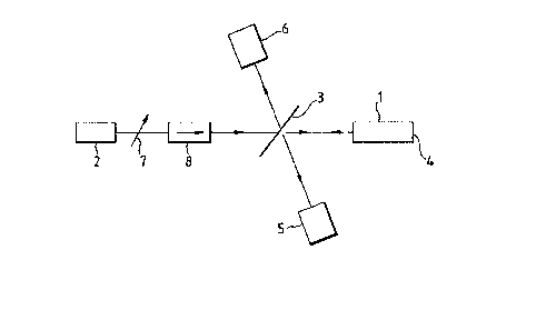
Referring to Figure 1, the switch comprises a
doubIe channel planar buried haterostructure (DCPBH) laser
30amplifier 1 used in reflection. An optical switching
signal is provided by a tunable laser source 2, in
combination with an attenuator 7.
A beam splitter 3 mounted between the source 2 and
the amplifier I deflects a portion of the optical output of
35the source 2 to a switching signal monitor 6, and a portion
of the output of the amplifier 1 to an output signal
,
monitor 5. Interaction between the source 2 and the
amplifier 1 is prevented by an isolator 8, between the beam
splitter 3 and the source 2, and an attenuator 7 is used to
modify the output of the source 2 to produce a controllable
switching siqnal. (The source 2 and attenuator 7 are
provided in the present embodiment to mimic an incoming
signal which would in practice comprise a signal carried by
for instance an optical communications system in
operational use).
The amplifier 1 is a Fabry-Perot DCPBH laser
without anti-reflection coatings, 200~m long, comprising
InP with an InGaAsp active layer. Threshold current at
room temperature is 15.7mA and the emission wavelength
1508nm.
The laser has an active cross section of 0.4~m2~
The source 2 is a grating tuned external cavity
laser which provides a single-mode signal. This laser is
an anti reflection coated ridge waveguide laser, tunable in
the range from 1450 to 1580nm inclusive, again comprising
InP with an InGaAsp active layer.
The isolator 8 is provided by two isolating
devices, giving together 60dB isolation. Maximum coupled
powers from the source 2 to the amplifier 1 of a few
hundred ~W can be obtained, as deduced from the resultant
photocurrent induced in the ampliEier 1. The beam splitter
3 comprises a simple uncoated glass slide, and a fast PIN-
pre amp combination (not shown) provides temporal
resolution of lOOpsecs to allow switching speed
measurements by directly modulating the tunable source 2.
Methods of operating the switch will now be
described and results discussed.
The source 2 is tuned to produce a signal detuned
from a cavity resonance, showing strong gain, of the
amplifier 1 by an amount corresponding to a single-pass
(i.e. non-reflected) phase change of -0~3~, or 30% of the
difference between adjacent cavity modes. By applying
'
. ~ .
~.Z~ 4
selected combinations of driving current and switching
signals, the amplifier 1 can be caused to show optical
bistability in three different manners.
Referring to Figure 2a, using a drive current
which produces a material gain in the amplifier 1 of 0.95
times the lasing threshold gain, the amplifier 1 shows
behaviour of a first type which can be exploited as a
logical AND/OR gate. In the Figure, the amplifier output
signal intensity "Io" is plotted against the input
switching signal intensity "Ii", both intensities being
normalised using a scaling intensity "Is". It can be seen
that "Io/Is" shows an anticlockwise hysteresis loop 10 in
response to "Ii/Is", which loop 10 includes a step increase
9 in response to increasing "Ii/Is". If "Ii/Is" increases
from a value below the step increase 9 (less than B) to a
value above it ~more than C), "Io/Is" will switch from a
value in a low range (less than b) to a value in a
relatively high range (more than c). These two ranges for
"Io/Is" can then be used to represent "logic O" and "logic
1" outputs respectively.
If l'Ii/Is" represents the sum of two incoming
binary logic signals, (i) and (ii), the values of the
incoming signals representing "1" and "0" inputs can be
selected as follows:
1 AND qate operation
(i) and (ii) each have zero or insignificant intensity for
a "0" input;
(i) and (ii) each alone have an intensity equivalent to
"Ii/Isf' in a range (A to B) which lies within the
hysteresis loop 10 for a "1" input such that (i) and (ii)
1'1" inputs summed have an intensity equivalent to "Ii/Isi'
more than C;
giving the following logic table:
.
'
z~
(i) (ii~ "Io/Is"
O O o
0 1 0
1 0 0
1 ~
2 OR qate operation
10 (i) and (ii) each have zero or insignificant intensity for
a "0" input;
(i) and (ii) each alone have an intensity equivalent to
"Ii/Is" more than C for a "1l' input;
giving the following logic table;
~i~ (ii) "Io/Is"
O O O
0
0
It can be seen that the step increase 9 occurs as
part of a hysteresis loop 10 which includes a step decrease
11. The step decrease 11 applies when "Io/Is" has dropped
to a critical value c'. If the range of values for "Io/Is"
greater than c' is taken to represent a "logic l" outpu~,
then it can be seen that the switch offers ~ND gate
operation as above but with a memory characteristic. This
is because once "Io/Is" has shown a "logic 1" output, if
only one of the incoming signals drops to a "0" input,
"Io/Is" will continue to show the "logic 1" output. Only
when both incoming signals have dropped to a "0" input will
"Io/Is" reach~the ~tep decrease 11 and switch to a "logic
0" output. This is represented by the following logic
table;
3 AND ~ate oPeration with memory character:istic
(i) and (ii) having values in the sequential order of
: combinations: shown: ;
~: ~ 40
, ~
,
(i) -- (ii) "Io/Is"
O O O
0 1 o
1 0 0
0
O o _ o
. . _ _ _ . _ _ _ _
It will be understood that after the 1-1 combination of
values for (i~ and (ii), the combinations 1-0 and 0-1 are
interchangeable. Only the 1-0 combination has been shown
here however, and in following logic tables with memory
characteristics, to reflect the practical danger that
switching sequentially from 1-0 to 0-1 might take the
ampli~ier through a 0-0 condition, and so cancal the memory
characteristic.
Further, the memory characteristic can be modified
by applying an optical bias (iii) to the ampli~ier 1, and
changing the values of (i) and (ii) for a "1" input, as
follows:
4 AND qate operation with biased memory~ acteristlc
Optical bias (iii) has an intensity equivalent to "Ii/Is"
slightly above A;
(i) and (ii) each have zero or insignificant intensi.ty for
an "0" input;
(i) and (ii) each alone has an intensity for a "1l' input
such that (iii) plus that intensity is equivalent to
"Ii/Is" less than B but (iii) plus two times that intensity
is equivalent to "Ii/Is" more than C;
giving the following logic table;
:
::
.,~
~, :
9 ~ ~ 0 4~
bias fiii) ti) ,_fil), "Io~Is"
on O O O
on O l O
on 1 O O
on
on 1 o
on O O
off o_ O O
An optical bias (iii) can also be used to produce
OR gate operation with a memory characteristic as follows:
OR gate ,operation_with biased memory characteristic
Optical bias (iii) has an intensity as undar 4 above;
(i) and (ii) each have zero or insignificant intensity for
a "O" input;
(i) and (ii) each alone have intensity for a "l" input such
that (iii) plus that intensity is equivalent to "Ii/Is"
moxe than C;
giving the fallowing logic table;
-
-
bias (iii~ (i) (ii) "Io/Is"
on O O O
on 0
on 1 O
on
on 1 O
on O O
off O O 0
Referring to Figure 2b, using a drive currentwhich produ~ces a material gain in the amplifier 1 of 0.65
times the lasing threshold gain, the amplifier l shows
behaviour of~a second type which can be exploited as a
logical NAND/NOR gate. Again, in the figure~ "Io" is
plotted against "Ii", both being normalised against "Is".
It can be seen that in this case "Io/Is" shows a clockwise
hysteresis loop 12 in response to "Ii/Is", which loop 12
includes a step decrease 13 in response to increasing
-~ ~2~f~
"Ii/Is", and a step increase 14 in response to decreasing
"Ii/Is".
By selecting ranges of values of "Io/Is" as "logic
1" and "logic 0" outputs, for instance from G to H and from
E to F respectively, it can be seen that the amplifier 1
will act as a switch as described above but with reversed
logical outputs. Because of the direction, and position
with regard to zero "Io/Is", of the hysteresis loop 12, it
is preferable to use an optical bias (iv). Without an
lo optical bias (iv), there are two ranges of values of
"Ii/Is", g to h and g' to h', which will produce a "logic
0" output value of "Io/Is". To avoid ambiguity, in case
for instance of noise or malfunction, the optical bias (iv)
should be equivalent to a value of "Ii/Is", greater than
h', which will bring the switch into an operating range
excluding the range of values of "Ii/Is", g' to h', which
introduces ambiguity. Employing an optical bias (iv), the
amplifier offers the following modes of operation:
6 NAND qate o~eration
Optical bias (iv) has an intensity e~uivalent to "Ii/Is",
just above e' which can produce a "logic 1" output of
"Io/Is", but lies well below the hysteresis loop 12;
incoming binary logic signals (i) and (ii) each have zero
or inæignificant intensity for a "O" input;
(i) and (ii) each alone have an intensity for a "1" input
such that (iv) plus that intensity is equivalent to "Ii/Is"
in the range, e' to e, which can produce a "logic 1" output
of "Io/Is" but lies below the hysteresis loop 12, but such
that (iv) plus two times that intensity is equivalent to
"Ii/Is" in the range, g to h, which produces a "logic 0"
output of "Io/Is": .
giving the following logic table;
~.2~o~
bias (iv~ ri) (ii) 'IIoJIs''
on 0 0
on 0
on 1 0
on 1 1 0
By changing the relative values of the bias (iv) and each
incoming binary logic signal (i) and (ii), NAND gate
operation with a memory characteristic can also be
achieved, as follows:
7 NAND gate operation with biased memorY character stic
Optical bias (iv) has an intensity as under 6 above;
incoming binary logic signals (i) and (ii) each have zero
or insignificant intensity for a "0" input;
(i) and (ii) each alone have an intensity for a "1" input
such that (iv) plus that intensity is equivalent to "Ii/Is"
in a range, e to f, within the hysteresis loop 12, while
(iv) plus two times that intensity is equivalent to "Ii~Is"
in the range, g to h, which produces a "logic 0" output of
"Io/Is";
giving the following logic table, (i) and (ii) having
values in the sequential order of combinations shown;
bias (iv) (i) (ii) "Io/Is''
on 0 0
on 0
on l 0
on 1 1 ~ 0
on 1 0 O :
. _on O O
: :
8 NOR gate operation
Optical bias (iv) has an intensity equivalent to "Ii/Is" in
the range e' to e, just below the hysteresis loop 12;
(i) and (ii) each have zero or insignificant intensity ~or
a "0" input;
~.
13
(i) and (ii) each alone have intensity for a "1" input such
that ~iv) plus that intensity, or plus two times that
intensity, is equivalent to "Ii/Is" in the range, g to h,
which produces a "logic 0" output of "Io/Is";
giving the following logic table;
bias~ iv) li) (ii) "Io/Is"
on 0 0
on o 1 0
on 1 o 0
on 1 1 O
on 1 0 0
on _ 0 O 1 _
It will be noticed that NOR gate operation as
above shows no memory characteristic. However, by
introducing a higher value of the optical bias (iv), both
NAND and NOR operation show a memory characteristic, as
follows:
9 NAND qate _operation with _modified biase~m~m~y
characteristic
Optical bias (iv) has an intensity equivalent to "Ii/Is" in
the range, e to f, which lies within the hysteresis loop
12;
(i) and (ii) each have intensities as under 7 above;
giving the following logic table, (i) and (ii) having
values in the sequential order of combinations shown;
_
bias (iv) (l! (ii) "Io/Is"
on O 0
on 0
on . 1 O
on 1 1 0
on 1 O O
on O O O
- oPf O 0 reset_ _ _
. ~
~2~
14
It will be seen that when the optical bias ~iv)
and both (i) and (ii) are at zero, "Io/Is" is merely reset
rather than giving an output value since the ranges of
"Io/Is" selected for "logic 0" and "logic 1" outputs E to
F and G to H, do not include zero.
NOR ~ate operation wikh memory characteristic
Optical bias (iv) has an intensity as under 9 above;
(i) and (ii) each have intensities as under 8 above;
giving the following logic table;
bias Liv) (i) (ii) "Io~Is
on 0 0
on O 1 0
on 1 O O
on 1 l 0
on 1 0 0
on o O o
off _ 0 Q reset
Referring to Figure 3, it is thought that the
switching behaviour described above is derived from a
relationship between "Io/Is" and "Ii/Is", as affected by
the driving current supplied ko the amplifier 1. This
relationship has been plotted for a range of values of
driving current, represented by the ratio of the amplifier
gain in operation to the lasing threshold gain of the
amplifier, g/gth.
~ t can be seen that for higher values of g/gth of
0.85 and above, the relationship shows an open, upwards
loop 15. For lower values, of 0.7 and below, the
relationship shows an open, downwards loop 16. In fact the
downwards loop 16 should occur for values of g/gth of up to
and including 0.74~ It is thought to be these loops 15,
16, within which the value of "Io/Is" is bistable, which
introduce the hysteresis loops 10, 12 o~ Figures 2a and 2b.
~*
~2~
(Bistability rather than tristability occurs because the
linking portions of the loops 15, 16, with opposite Ii/Is
direction, are unstable).
For a range of values of g/gth lying between 0.74
and 0.85, the relationship shows a closed loop 17, and the
amplifier 1 shows behaviour of a third type. Referring to
Figure 4, this closed loop 17 indicates a double hysteresis
loop 18 with two step decreases in "Io/Is", a first part 19
of the loop 18 being traversed in a clockwise direction
(for increasing input) and a second part 20 being traversed
in an anticlockwise direction (for decreasing input).
To convert the normalised intensities of Figures
2 to 4 to optical input power levels, for the amplifier 1
described above the scaling intensity Is has a value of
about 8 x 10⁵ W/cm2. Over the active cross section of the
amplifier diode, this corresponds to a factor 8 x 109 x 0.4
x 1012 W, or 3.2 x 10³ W. Hence it can be seen from Figure
3 that at the higher value of g/gth, 0.95, the open,
upwards loop 15 occurs between values of approximately 16~W
and 64~W for Ii. However, at the lower value of g/gth,
0.7, the open, downwards loop 16 occurs between values of
approximately 100~W and 120~W for Ii. It can be expected
that these higher values of Ii required to obtain optical
bistability are a result of the associated lower value of
g/gth. There is, here, a trade-off. If the source 2 is
tuned to produce a signal which is closer to a cavity
resonance of the amplifier 1, optical bistability is
achieved at lower values of Ii but the loops 15, 16 are
reduced in size. Conversely, if the detuning of the source
2 is increased, optical bistability is achieved at higher
values of Ii but the loops 15, 16 are larger.
Another factor which affects the size of the loops
15, 16 and the values of Ii associated with optical
bistability is the reflectivity of the reflecting facet of
the amplifier 1. That is, the "hack" facet of the
amplifier 1 which acts neither as an input nor as an output
16
port. By increasing the reflectivity of this facet, for
instance by the use of a high-refl~ctivity coating, the
depth of the optical bistabilities produced can be
increased. That is, the ranges of values of "Io/Is" taken
to represent "logic o" and "logic l" outputs can be
selected to lie further apart. However, at the same time
the values of Ii at which optical bistability occurs
increase. (Uncoated, as in the arrangement of Figure 1,
the reflecting facet of the amplifier 1 has a reflectivity
of about 30~).
` Further information on the hysteresis loops of
Figure 3 can be obtained from the calculated spectral
response of the amplifier for fixed input power. Referring
to Figure 5, the spectral response curves plotted for a
range of values of 0O, the input signal phase detuning from
a cavity resonanca of the amplifier, for a fixed "Ii/Is" of
0.03, and for values of g/gth as marked, show loops 21
associated with the hysteresis loops of Figure 3 at gains
g/gth of 0.8 and 0.9. For gains g/gth of 0.7 and 0.6, the
spectral response curves resemble those seen for passive
Fabry-Perot devices.
The speed of switching of an optical switch
according to an embodiment of the present invention can be
assessed by looking at the device response to an optical
input signal varying sinusoidally with time.
Referring to Figures 6, 7 and 8, in each case
calculated optical output response is shown for a steady
state input signal (graph (a)), and for sinusoidal input
signals of periods equal to 4, 8 and 12 times the carrier
recomb-ination time o~ about 1.7nsecs (graphs (b) and (d)
raspectively). (A steady state signal in this context is
a signal whose repetition rate is of the order af KHz or
less). The value of g/gth is different for each Figure,
being 0.9, 0.8 and 0.7 for Figures 6, 7 and 8 respectively.
The first graph (a) of each Figure thus corresponds to one
of the plotted curves on Figure 3.
.
- ~ .
~ 2~
From the observed device response to the
sinusoidal signals, it would seem that the switching time
between stable gain states, at least where the optical
switch is being used as an AND/OR gate, is likely to be of
the order of the carrier recombination time. Hence the
maximum clock rate at which the switch will operate will be
limited by nanosecond switching times.
Intensity spikes 22 can be observed on the device
response curves. There are understood to stem from changes
in the material refractive index of the amplifier 1 due to
changes in the optical input intensity. In the case of
Figure 8, it can be seen that these spikes 22 are directed
downwards and are only vestigial.
Referring to Figure 9, optical switches 26
according to embodiments of the present invention can be
used in an array for instance in optical time-division
switching. Using LiNbO3 directional coupler matrices to
provide a read gate 23 and a write gate 24, four 64 Mb/s
digitally encoded colour video signals which are time
multiplexed in bit-interleaved ~orm are applied to a time
switch 25 comprising optical switches 26 according to
embodiments of the present invention. The write gate 24
supplies the 256 Mb/s time-multiplexed signal to each
switch 26 in turn. The switches 26 each store the optical
signals for a frame period. The stored signals can then be
read out according to a required sequence and time
switching has been accomplished.
The optical switches 26 can be reset by the use of
optical clock signals.
In another application, optical switches according
to embodiments of the present invention could be used in
optical regenerators. Using an incoming digital signal and
clock pulses as the two incoming binary logic siynals ti)
and (ii) referred to above, the incoming digital signal can
in effect be regenerated and sent onwards.
~;
.
-
18
It is not necessary that an embodiment of the
present invention should include all the features described
above. In particular it is not necessary that a Fabry-
Perot laser diode be used as the amplifier 1. Instead, for
instance, a DFB laser diode may be used.