Note: Descriptions are shown in the official language in which they were submitted.
5~
The invention relates to a control device of two bipolar
transistors connected in series between conductors of a
direct operating voltage supply and having a center output
point to form an inverter arm, each transistor having a base
s control unit supplied by a direct control voltage source.
To each phase of the inverter there corresponds an arm
having two transistors in series subjected to the operating
voltage which generally reaches several hundred volts. Each
transistor has associated with it a base control capable of
supplying a base current of several amps at a low voltage,
notably a few volts, to make the transistor conducting and a
low negative voltage blocking the transistor. These control
voltages are generally speaking derived Erom the high
operating voltages, which gives rise to insulation problems
in the case of the inverter arm with two trans:istors
connected in series.
The object of the invention is to achieve a simplified
control of the transistors of an inverter arm capable of
withstanding the high operating voltages.
According to the present invention, there is provided a
control device comprising:
a first and a second bipolar transistor connected in
series, and connectable between first and second conductors
of a D.C. voltage supply, a center point between said first
and second bipolar transistors forming an inverter output;
first and second base current control units connected
to bases of a respective one of said first and second
bipolar transistors, said control units each being supplied
by a control voltage source, and each being referenced to a
different ground potential:
a power supply unit includin a transformer having a
,.................................................. ~
~29~
primary winding connectable to said conductors of said D.C.
voltage supply, and first and second separate secondary
windings, each second winding supplying, through respective
rectifiers, a respective one of the control units with a
substantially constant D.C. control voltage, said power
supply unit further comprising a voltage regulator including
a tertiary winding of said transformer, a device controlled
by the tertiary winding and a switch in series with said
primary winding, said switch in series with said primary
winding, said switch being controlled by said device.
Thus, each transistor is provided with its own control unit
at the potential of the transistor and the two control units
are supplied by a single power supply unit, which respects
lS the galvanic insulation of the two control units, by means
oE a power supply -transformer w:ith two independent secondary
windings, each operating in conjunction with one o-E -the
control units. This galvanic separation ensures that the
voltage difference of several hundred volts, to which the two
control units of the two transistors are subjected, is
withstood. The power supply transformer comprises a primary
winding common to the two secondary windings and voltage
regulation is performed by a regulator comprising a static
switch inserted in the transformer primary circuit. This
static switch is controled by a tertiary winding of the
transformer via a device causing the static switch to open
periodically to regulate the output voltage. Each secondary
winding comprises a center tap and diode rectifiers are
connected to the end terminals of this secondary winding to
supply the positive and negative control voltages,
respectively for conducting and blocking the transistor.
Preferably, a capacitor is connected in series with a diode
to the terminals of the transistor, between the collector
. ~
-- 3
and the emitter. Any overvoltage occurring at the
transistor terminals is branched off into the shunt circuit
formed by the diode and capacitor, the latter absorbing the
overvoltage by charging. The capacitor is discharged by
means of a resistive circuit connecting the capacitor to the
operating voltage supply of opposite polarity.
In a preferred embodiment of the invention, each control
unit comprises means of selectively connecting the
associated transistor base via a resistor to a positive
control voltage supply to make the transistor conducting and
of connecting the transistor base to a negative control
voltage supply to block the transistor, said connecting
means of the transis-tor base to the posit:ive voltage supply
comprising, connected in serles, a current regulator
delivering a constant current and an energy storage inductor
to increase the rise speed of -the transistor base current on
a conduction order and to counteract the emitter
interference inductance.
Thus, the current regulator accurately defines the value of
the base current ensuring conduction of the transistor,
whereas the inductor counteracts or cancels the interference
effect of the emitter impedance, this inductor constituting
an energy store available when the transistor becomes
conducting.
Preferably, the current regulator comprises a current sensor
which controls a regulating amplifier controling a static
switch inserted in the base control circuit. Blocking of
the transistor is achieved by closing of a static switch
which branches the current delivered by the current
regulator off to the voltage supply by simultaneously
establishing a negative base current via a resistor to the
negative voltage supply. This negative voltage supply
polarizes the transistor base to keep the latter blocked.
According to the present invention, there is also provided a
control device comprising:
a first and a second bipolar transistor connected in
; series, and connectable between first and second conductors
of a D.C. voltage supply, a center point between said first
and second bipolar transistors forming an inverter output;
and
first and second base current control units connected
to bases of a respective one of said first and second
bipolar transistors, said control units each being supplied
by a control voltage source, and each being reEerenced to a
different ground potential, each control unit including
means for selectively connecting a base of the respective
bipolar transistor to a positive D.C. control voltage supply
through a resistor to turn the respective bipolar
transistor on and for connecting said base of the respective
bipolar transistor to a negative D.C. control voltage supply
to turn the respective bipolar transistor of said means for
selectively connecting including a current regulator for
delivering a constant current, connected in series with an
energy storage inductor, sald current regulator comprising a
sensor of the current flowing throught the inductor, a
regulating amplifier controlled by said sensor and a switch
controlled by said amplifier to maintain a mean base current
at a constant value;
; a power supply unit including a transformer with a
primary winding connectable to said D.C. voltage supply and
first and second separate secondary windings, each second
winding supplying, through respective rectifiers, a
respective one of -the control units with a substantially
constant D.C. control voltage.
- 3b -
Brief description of the drawings
Other advantages and features will become more clearly
apparent from the following description of an illustrative
embodiment of the invention, given as a non-restrictive
example only and represented in the accompanying drawings,
in which:
- Figure 1 represents the wiring diagram of an inverter arm
with two transistors with their control circuit;
- Figure 2 represents the wiring diagram of the power supply
unit of the control circuits according to figure l;
- Figures 3 and ~ rep.resent the wiring diagram of a transistor
control unit respectlvely :ln the conducting and blook:ing
position;
/
~ .
, ':
~2~
- Figure 5 shows the variation of the base con~rol current of a
transistor according to figure 1 ;
- Figure 6 illustrates the variation of the transistor emitter
base voltage.
Description_of the preferred embodiments
''
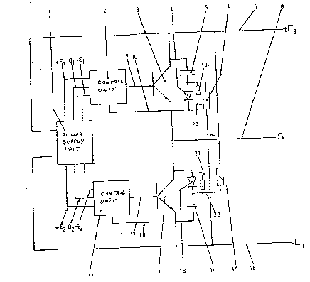
A high D.C. electrical voltage ~E3, -E3 is applied to conductors
7, 16 by a voltage source (not represented), for example a
battery or a rectifier. An inverter.arm made up of two power
transis,tors 3, 12 electrically connected in series is connected
to the conductors 7, 16 and an output conductor 3 is connected
to the connecting point of the two transistors 3, 12 b When the
transistor 3 connected to the ~E3 voltage is conducting, the
output S goes to the ~E3 potential whereas when t:he transistor
12 is conducting, this output goes to the -E3 potential in a
manner well known in the art. Each transistor 3, 12 is connected
to a control unit ~, 11, on the one hand by a conductor 9, 17
connecting the base of.the transistor to the control unit 2, 11
and on the other hand by a conductor 10, 18 connecting the
emitter of the transistor 3, 12 to the control unit 2, 11. The
control units 2, 11, which will be described in detail further
on, control the alternate conduction and blocking of the
transistors 3, 12 to generate an A.C. voltage on the output
conductor 8. The D.C. voltage +B3, ~E3, which can reach several
hundred volts, is also applied to a power supply unit 1
supplying a power supply voltage of a few volts to the control
units 2, 11 Referring more particularly to fi~ure 2, it can be
seen that the power supply unit 1 comprises a transformer whose
primary winding 52 is connected to the conductors 7, 16, a
static switch 55 being inserted in the primary circuit. The
static switch 55 belongs to a voltage regulator of a known type,
represented very schematically in the figure and comprising a
tertiary winding 53 of the transformer which controls a device
54 controling the static switch 55~ The transformer comprises
9~
two distinct secondary windings 56, 60, each having a center tap
57, 61 supplying the control output O voltage 01, 02. The ends
of the secondary windings 56, 60 supply the output voltages ~El,
-El ; +E2, -E2 via diode rectifiers 58, 59 ; 62, 63. These
control voltages delivered by the transformer are a few volts,
in this case only a fraction of the operating voltage +E3, -E3.
~he control voltages +El, 01, -El delivered by the secondary
winding 60 supply the control unit 2 of the transistor 3 whereas
the voltages +E2~ 02, -E2 delivered by the secondary winding 56
supply the control unit 11 of the transistor 12. The separation
of the secondary windings 56, 60 ensures insulation between the
contro~ units 2, 11 which can be at different high potentials~
A shunt circult comprising a capacitor S and a diode 4
electrically connected in series i5 connected to the terminals
of the transistor 3, the capacitor 5 being connected on the one
hand to the collector of the transistor 3, and on the other hand
to the anode of the diode 4 whose cathode is connected to the
emitter of the transistor 3. The connecting point of the
capacitor 5 and of the anode of the diode 4 is further connected
by a resistor 6 to the -E3 voltage conductor 16. There is
connected to the terminals of the diode 4 a circuit comprising a
resistor 19 and a capacitor 20.. Similarly, the transistor 12 is
shunted by a circuit comprising a diode 13 and a capacitor 14,
the anode of the diode 13 being connected to the collector of
the transistor 12 whereas the capacitor 14 is connected to
emitter of the transistor 12. The connecting point between the
diode 13 and the capacitor 14 is connected by a resistor 15 to
the ~E3 voltage conductor 7. The diode 13 is shunted by a
circuit comprising a resistor 22 and a capacitor 21. The shunt
circuit with capacitors 5, 14 and diodes 4, 13 in series
protects ~he transistor 3, 12 against overvoltages, the resistor
6, 15 keeping the capacitor 5, 14 charged.
Only the control unit 2 associated with the transistor 3 is
described hereafter referring to figure 3, the control unit 11
~L2~5~2
of the transistor 12 being strictly iclentical. The base of the
transistor 3 is connected to the conductor 31 at +El voltage by
a circuit 9 comprising a static switch 32, an inductor 34 and a
diode 35 electrically connected in series. The diode 35 is
shunted by a resistor 36~ The static switch 32 belongs to a
current regulator comprising a sensor 33, which controls a
regulating amplifier 30 which controls the static switch 32.
When the +El and -E1 voltages are applied to the conduc~ors 31
and 41, when the circuit is started up, the static switch 32 is
normally closed and the current flowing through the sensor 33
increases up to a first threshold, called the upper threshold~
As soo~ as this threshold is reached, the regulating ampli~ier
30 causes the static switch to open and the current flowiny
through the sensor decreases until ~it reaches a second
threshold, called the lower threshold, bringing about reclosing
of the static switch. The current regulator output current
therefore varies between the two above-mentioned threshold
values in such a way that its mean value is maintained constant.
This current regulator 30, 32, 33 therefore delivers a constant
current Il to control conduction of the transistor 3. The
emitter of the transistor 3 is connected to the O voltage, 01
and the connecting point of the inductor 34 and of the anode of
the diode 35 is connected by a static switch 38 to the conductor
~1 at El control voltage. The anode of a return diode 40 is
connected to the conductor 41 at -El voltage, the cathode of
this diode being connected to the connecting point of the sta~ic
switch 32 and of the ind~ctor 34.
In the open position of the static switch 38, represented in
figure 3, the current Il, kept at a constant value by the
current regulator 30, 32, 33, recloses via the inductor 34, the
diode 35 and the base of the transistor 3 in the power supply
Olo The transistor 3 is conducting, the diode 40 ensuring the
current feedback during the blocking phases of the switch 32. In
the closed position of the switch 38, represented in figure 4,
the current Il is drawn off by this switch 38 to the conductor
41, whereas a negative base direct current I2 is established via
the resistor 36 and the switch 38 to the conductor 41. This
negative direct current causes blocking of the transistor 3. The
base of the transistor 3 is polarized via the resistor 36 at ~he
voltage -El keeping the transistor 3 blocked.
It is worthwhile recalling that control of a transistor base
imposes the following conditions :
1) delivering a positive direct control current of a precise
value Il durin~ the transistor conduction time ;
2) achieving a fast base current rise time at the moment the
transistor becomes conducting ;
3) achieving a fast base current fall time at the moment the
transistor is blockea
4) delivering a negative direct current I2 of a precise value
during the transistor base blocking time ;
5) applying a negative direct voltage -El during the time the
transistor is blocked.
The emitter circuit of the transistor 3 presents an in~erference
inductance which tends to oppose the establishment of the base
current I~ making the transistor 3 conducting. According ~o the
present invention, this interference inductance is counteracted
by~the inductor 34 which constitutes an energy store imposing a
high-speed increase of the base current IB when the switch 38
opens, in spite of the presence of the emitter interference
inductance The value of the current Il is determined with
accuracy by the curr~n~ regulator 30, 32, 337 It is worthwhile
noting that the control current Il which can reach several amps
does not flow through any resistors and that ~he power
dissipated in the control circuit is particularly low and a
,
`''` ~1 2~5~ ~
~raction of that of standard control circuits, The switches 38
of the control circuits 2, 11 are controled by standard devices
to make the transistors 3, 12 alternately conducting and to
generate an alternating current of predetermined frequency. It
is pointless describing these control circuits of the switches
38 which may be of any kind.
Figures 5 and 6 illustrate respectively the variation of the
base current IB and of the emitter base voltage of the
transistor 3 confirming that the conditions set out above are
met.