Note: Descriptions are shown in the official language in which they were submitted.
/t^1~
-- 1 --
FIELD OF THE INVENTION
The present invention relates to a power
factor correction system and to a rnet:hod for connecting
and disconnecting same. The invention also includes a
fuse assembly for the power factor correction system of
this invention.
BACKGROUND OF THE INVENTION
With the increase of electeicity costs in
recent yearsr large electricity consurners have
attempted to reduce these costs by improving the power
factor of their industrial and commercial
establishments. It is well known that a low power
factor is created by the presence of induction motors
and particularly by motor drives that employ
thyristors. The latter are being used more and more
because of the ease and accuracy of attaining speed
control.
<
The power factor of an establishment can be
raised to the desired level by installing capacitors.
However, because the power dernand varies throughout the
day, the number of capacitors in service must be varied
to maintain the power factor at the desired level. As a
- 2 - 1295~ ~
result, capacitors must continuously be switched in and
out.
When a capacitor is switched across an AC
line it is well known that a large transient current of
oscillatory nature flows for a short time, typically
- for less than 0.1 second. At the same time, the peak
transient voltage across the capacitor can momentarily
reach values that are twice as high as those
` 10 encountered in normal operation. The extremely large
transient current darnages the switch contacts
Furthermore, the large current combined with the
overvoltage may cause premature failure of the
capacitors.
The peak transient current is particularly
large when a capacitor is switched across a line that
already has capacitors installed across it. The peak
current is then limited only by the resistance and
inductance of the leads connecting the incoming
capacitor to the line. The resulting peak currents can
reach values 100 times greater than normal.
:
When the capacitor is disconnected from the
line, there is usually no substantial arc while the
` switch contacts are separating. As a result, opening
.,
the circuit of a capacitor that is directly across the
.i .
~:
,, ", .. . .
~, .
- 3 - ~ ~ 5 ~ ~
line presents no problem as regards contact wear
However, if the switch opens slowly, the interrupted
current may be re-established when the contacts are
slightly apart. This creates a large transient restrike
current which is even greater than the transient
current when the capacitor was switched onto the line.
This restrike current may repeat several times, with
damaging effect on the switch contacts However,if the
switch contacts separate quickly enough! the restrike
phenomenon does not occur.
In view of explanations that will be given
later on, it must also be stated that if a resistor is
connected in series with a capacitor, an arc will be
15drawn when the switch disconnects the capacitor from
the AC line. The magnitude of the arc becomes greater,
the larger the voltage drop across the resistor at the
~moment the circuit is interrupted. Thus, the contact
Jwear on switch opening is greater than if no resistor
20were present. The same remarks apply when an inductance
is connected in series with the capacitor.
In view of further explanations that will be
given later on, it must be stated that electronic motor
25drives produce harmonic currents in the AC line. These
currents have frequencies that are odd multiples of the
, .
line frequency. On a 60 Hz line, the principal harmonic
,..
.
_ 4 _ ~ %~5~ 1~
currents are the 5th , 7 h and 11th, corresponding to
300 ~z, 420 Hz and 660 Hz. Other harmonic currents are
also present, but their effect is usually
insignificant. The magnitude of the harmonic currents
is directly related to the power drawn by the electric
drive.
Corrective measures using resistors.
In order to reduce the transient current when
a capacitor is switched across the line by a switch
(Sl), a resistor may be connected in series with the
capacitor. The presence of a resistor also eliminates
the transient overvoltage across the capacitor, and
this method of solving the overcurrent and overvoltage
problem is well known. A resistor having a relativity
high resistance can reduce the peak transient current
to a reasonabIe value. However, such a resistor will
cause a substantial arc to be formed when the capacitor
is disconnected from the line by opening a first switch
(S13. Furthermore, the sustained heat loss and energy
loss of the resistor while the capacitor is in service,
may not be economically acceptable. As a result, it is
common practice to short-circuit the resistor with a
second switch (S2) shortly after the capacitor is
switched into service.
~2g~6
-- 5
In -the course of investigation, it has been
discovered that when switch (S2) closes, a relatively
large transient current is again produced. The
magnitude of this current increases with the resistance
of the resistor. More precisely, the peak transient
current depends upon the voltage drop that existed
across the resistor just prior to the moment when
switch (S2) was closed. In effect, it is as if the
capacitor were switched across a line whose voltage is
equal to the voltage drop across the resistor.
'rhe said transient current can damage the
contacts of switch (S2). Thus, in order to reduce the
contact wear of switch (S2), the resistor must possess
a relatively low resistance. But a low resistance tends
to raise the peak transient current when switch (Sl) is
closed. Thus, a compromise must be struck so that the
contact wear of both switch (Sl) and switch (S2) is
acceptable. In brief, two transient inrush currents are
produced when a resistor/capacitor circuit is used, and
the value of the resistor must be selected to optimize
; the contact wear on the two switches.
,
Corrective measures using inductors.
An inductor is sometimes used in series with
a capacitor to limit the transient current. The
- 6 ~ ~ 2~ 6
advantage of the inductor is that it dissipates very
little heat (compared to a resistor) and, consequently~
it can be left permanently in series ~ith the capacitor
while the latter is in service. However, because the
inductor carries the full capacitor current it tends to
be large and rather expensive. Furthermore, the
presence of the inductor does not, in any way, reduce
the transient overvoltage that occurs across the
capacitor when it is switched onto the AC line. As a
result, the capaci.tor can still suffer damage after
repeated switching.
The presence of the inductor can also produce
serious resonance effects when the factory or
industrial establishment contains electronic motor
drives. The reason is that the harmonic currents
generated by the drives may be amplified many times
depending upon the relative magnitude of the inductors,
; capacitors and other inductive devices (such as
electric motors) that happen to be in operation at a
given time. This amplification is due to resonance and
it can cause large harmonic currents to flow in the
capacitors, as well as in other parts of the electrical
system of the industrial establishment, notably the
service entrance transformer. The large harmonic
currents can also produce overvoltages and voltage
distortion in the electrical system.
~".
(
, '- . .
_ 7 _ ~2~S~ 1~
OBJECTS AND STATEMENT OF T~E I~YE~TIOM
Therefore, it is an object of this invention
to provide a power factor correction system with an
improved configuration per~nitting to use switches of
reduced current capacity than the prior art devices.
Another object of the present invention is to
provide a power factor correction system which is
compatible with modern electronic motor drives~
Another object is a method for operating the
power factor correction system of this invention, which
method reduces the erosion of the switch contacts.
Another object is to reduce the size of the
inductors and resistors that are used to limit the
~'
inrush currents,
A further object of the invention is a novel
fuse assembly that may be used advantageously with the
power factor correction system of the present
~' invention.
` ?
, 25 The above objects are achieved by providing a
. power factor correction system comprising a capacitor
and a voltage and current limiting circuit (hereinafter
.,, - :
- 8 - ~ ~ ~ S~ 1~
"limiting circuit") for reducing the amplitude of the
transient currents and voltages in the capacitor. The
limiting circuit includes a branch consisting of a
resistor and an inductor connected in series. The
branch is active only for a given period of time;
during the steady state operation of the system, it is
by-passed.
Preferably, the limiting circuit includes a
; 10 branch consisting of a resistor, an inductor and a
first switch (Sl) connected in series, and a second
switch (S2) connected in parallel with said branch for
de-activating it by establishing a short-circuit.
When the power-factor correction system is
~` energized, (Sl) is closed first. When the resulting
transient voltages and currents have essentially
~ subsided and when, therefore, the potential across the
;~ inductor has dropped substantially (S2) is closed so as
to short-circuit the branch. The current rating of (Sl)
can, therefore, be relatively low since (Sl) carries
current only during a short period of time, typically
~ for one or two cycles. The presence of the inductor
;~ allows the use -of a resistor of relatively low
resistance and a corresponding low voltage drop across
- the resistor. As a result, a relatively low transient
` 1
!
'
.
- 9 -
current is produced when the contacts of (S2) close,
which reduces their wear.
To disconnect the power factor correction
system, (S1) is opened first, followed by the opening
of (S2). If the opposite sequence is followed, the
contacts of (S11 erode much faster because the presence
of the resistor and the inductor in the branch creates
an arc across (Sl) whenever (Sl) opens.
Preferabl~, the power factor correction
system of this invention is provided with a fuse in the
branch. The fuse comprises a fusible member adapted to
melt when a current with a given amplitude passes
therethrough for a given time. In order to reduce the
size of the fuse and yet allow it to clear a fault
quickly and without restriking, the fusible member is
mounted within a magnetic field, and substantially
cross-wise to the magnetic field. When current
circulates through the fusible member, a force is
exerted thereon with a direction perpendicular to the
; direction of the current and to the magnetic field.
; When the fuse begins to melt, the force blows both the
molten material and resulting arc and so the circuit is
interrupted quickly and effectively. The magnetic field
may be generated by a coil.
i
- 1 o - $;~5~
The power factor correction system of this
invention may be used with a single-phase system as
well as with a three-phase system. In the latter case,
the power-factor correction system includes a capacitor
bank in delta or in Y configuration and three limiting
circuits connected respectively between the three-phase
lines and the capacitor bank.
Therefore, the present invention comprises a
power factor correction system which in broad terms
includes:
- a capacitor; and
- a limiting circuit having a given
irnpedance, the limiting circuit limiting the
overvoltages and the overcurrents susceptible to occur
in the capacitor after the energizing of the power
factor correction system, the limiting circuit being
connected to one terminal of the capacitor and
including:
a) a branch having a resistor serially
connected to-an inductor; and
b) impedance reducing means operatively
connected to the branch for reducing the impedance of
the limiting circuit after a given period of time
following the energizing of the power factor correction
system.
;
2~s~ ~ ~
This invention also relates to a m~thod for
energizing a power factor correction system comprising:
- a capacitor; and
- a limiting circuit having a given
S impedance, the limiting circuit being connected to one
terminal of the capacitor and limiting the overvoltages
and the overcurrents susceptible to occur in the
capacitor after the power factor correction system is
energized, the limiting circuit including:
a) a branch including in series a
resistor, an inductor and a first switch means; and
b) a second switch means mounted in
parallel with the branch for short-circuiting the
branch after a given period of time from the energizing
of the power factor correction system, the first and
the second switch means being in opened position before
the energizing of the power factor correction system.
The method for energizing the power factor correction
system, in general terms, consists of the following
sequential steps:
- closing the first switch means thereby
allowing current to circulate through the branch, the
current creating a relatively high potential across the
inductor; and
~25 - closlng the second switch means when the
~potential has dropped substantially.
.' ~
' .~"
~'
- 12 - ~2~5~ ~
The present invention further relates to a
method for disconnecting the power factor correction
system, the method consisting, in broad terms, of the
following sequential steps:
- opening the first switch means; and
- opening the second switch means.
This invention also comprises a combined fuse
and inductor and resistor circuit for use in a power
factor correction system, the fuse and inductor and
resistor circuit comprising in its most general
aspects:
- an inductor adapted to generate a magnet.ic
field with a given direction when current circulates
therethrough; and
- a fusible member serially connected to the
inductor and being mounted within the magnetic field
and extending across the magnetic field, current with a
given direction being adapted to circulate through the
fusible member, when current circulates through the
fusible member and through the inductor a force being
exerted on the fusible member with : a d.irection
perpendicular to the direction of the magnetic field
and to the direction of the current in the fusible
member.
: ' :
..~
.. .. .
- 1 3 ~ ~.2$5~ ~
BRIEF DESCRIPTIOI~ OF DRAWINGS
A detailed description of preferred
embodiments of the present invention will be given
hereinafter with reference to the annexed drawings in
which:
Figure 1 is a diagram of a prior art power
factor correction system;
Figure 2 is a diagram of a single-phase power
factor correction system according to this invention;
Figure 3 is a diagram of a three-phase power
` 15 factor correction system according to this invention;
: ~ ~ Figure 4 is a diagram illustrating the
~, principle of operation of a fuse assembly according to
this invention; and
Figure 5 is an exploded view, partly
sectional, of an embodiment of the resistor-inductor
~ f
~;t~ and fuse assembly of this invention.
,~ Z5 Figure~ 1 illustrates schematically a prior
art power factor correction system such as the one
.~ : making the subject of US patent 1 939 064 issued
. December 12, 1933 to T. Kopczynski.
:?
'I .
1j
,
~S411~
- 14 -
PRIO~ A~T SYSTEM
The power factor correction system,
designated generally by reference numeral 1, is
connected to a single-phase line 2 The correction
system 1 comprises a capacitor 3 connected to a
resistor 4. A main switch 5 is in series with capacitor
3 and is utilized to switch correction system 1 across
the power line. A second switch 6 is mounted in
parallel with resistor 4. When the power-factor
correction system is to be energized, switch 5 is
closed first and resistor 4 limits the transient
current in capacitor 3. After a predetermined period of
time sufficiently long so that the capacitor current
and voltage have become stable, switch 6 is closed,
thus short-circuiting resistor 4 and avoiding continual
power losses.
However, when switch 6 closes, and as
previously explained in the disclosure, the voltage
drop Er across resistor 4 gives rise to a large
transient current which flows through the contacts of
switch 6, increasing the wear thereof.
`
Further~nore, during the steady-state
operation of the power factor correction system 1, both
switches 5 and 6 carry the full current of the
- 1s - ~,.~5~
capacitor and consequently they must both have a
relatively high current rating.
DESCRIPTION OF PREFERRED EMBODI~ENTS
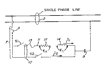
Referring now to figure 2, a single-phase
power factor correction system 7, according to this
invention, comprises a capacitor 8, and a main fuse 9
connected in series with a current-limiting circuit 10.
The latter includes switch (S2) and a branch 11
comprisiny in serial connection a switch (Sl), a
resistor 12, a fuse 13 and an inductor 14. Switch (S2)
is connected in parallel with branch 11 for
short-circuiting same during the steady state operation
of the power factor correction system 7.
Figure 3 illustrates a three-phase power
factor correction system, according to the present
invention, connected across the three-phase lines 15 of
an industrial or commercial establishment. To each
phase line A, B, C is connected a limiting circuit 1~,
already described. A capacitor bank 16 co~posed of
three capacitors 8 is connected to the limiting
circuits 10. The capacitor bank has a Y configuration.
The capacitor bank may also have a delta
configuration.
~, ~
''
~2~5
-- 16 --
Figure 4 illustrates schematically an
embodiment of branch 11 which comprises the inductor 14
formed by a coil of conduc~ive copper wire 17 having a
given intrinsic resistance which constitutes resistor
12. The resistance of resistor 12 may be changed by
varying ~he cross section of wire 17, as is well known
in the art.
Fuse 13 is in serial connection with inductor
14 and comprises a fusible member 18 adapted to melt
when the current passing therethrough exceecls a
predetermined I2t limit. Fusible member 18 lies within
and across the magnetic field generated by inductor 14.
The direction of the magnetic field is designated by
the arrow M when current I passes in the direction
shown through fusible member 18. When current I flows
in the direction designated by arrow I, a force F is
exerted on fusible member 18. According to Fleming's
right-hand rule, the direction of force F is
perpendicular to the direction of the current in the
fusible member and also perpendicular to the direction
of the magnetic field. As a result, fusible member 18
is pushed away from the observer, and into the page of
~ Figure ~. Whenever an excessive current flows for a
:,. .
sufficient length of time through fusible member 18,
~ the force F will blow away the molten parts of fusible
;~ member 18 as well as the resulting arc. The arc becomes
~ . '
- 17 -
stretched, allowing the fault to clear rapidly and
completely, thus eliminating the possibility of an arc
restrike between the terminals 19, 20 of the fusible
member. The inductor thus fills a dual role: it limits
the peak transient current as previously described, and
provides the magnetic field to blow ou- the fuse.
Resistor 12 may also be constituted by an
independent resistor cQnnected in series with inductor
14. Fuse 13 may also be constituted by an independent
fuse of commercial make but not located in the magnetic
field oE inductor 14.
Referring now to Figure 5, the inductor,
resistor and fuse of the present invention are mounted
within a housing 21 comprising a capsule 22 of plastic
material into which is embedded inductor 14. As stated
earlier, resistor 12 is constituted by the intrinsic
resistance of the wire forming inductor 14. The fuse
terminals, 19 and 20, respectively project upwardly
from capsule 22, terminal 20 being connected to
terminal 23 of inductor 14. Between terminals 19 and 20
extends fusible member 18. Two leads 25 and 24
projecting from capsule 22 are in serial connection
with ~erminal 26 of inductor 14 and fuse terminal 19,
respectively.
.
, j
- 18 -
On the top face of capsule 22 is mounted a
spacing ring 27 of plastic material receiving a
transparent disc member 28 having openings 29 Ring 27
and disc 28 define a fuse chamber into which is located
fusible member 18. When fusible member 18 blows, the
: excess pressure generated in the fuse chamber is
eliminated through openings 29. Since disc member 28 is
transparent, the condition of fuse member 18 may be
easily inspected.
The power factor correction system of this
invention operates as follow.s. Referring to Fig~lre 2,
when the system is switched on, switch (Sl) is closed
first and a relatively large transient current I
begins to circulate through branch 11 and capacitor 8.
The peak value of transient current Il is limited to an
acceptable value by inductor 14 and resistor 12.
Compared to the voltage drop across resistor 12, the
transient voltage drop El across inductor 14 is
relatively high immediately after the closing of (Sl)
: because the current in branch 11 is changing very
~ rapidly. In order to prevent an excessive translent
; overvoltage across capacitor 8 during this period, it
is important to select appropriate values for both the
`1` 25 resistance of resistor 12 and the inductance of
inductor 14 in relation to the capacitance of capacitor
:~. 8.
/
- 19 - ~
Switch (S2) is closed when the voltage drop
El across inductor 14 has become negligible, which
occurs shortly after the closure of (S1). In effect,
inductor 14 and resistor 12 rapidly damp the transient
current Il in branch 11. When the transient has died
out, the potential be-~ween the contacts of (S2) is
constituted almost entirely oy the voltage drop Er
across resistor 12 which is of lesser value than the
potential across resistor 4 of the prior art device
shown in Figure 1. The reason is that, in the present
invention, inductor 14 permits the use of a resistor 12
of smaller resistance without affecting the current
limiting properties of branch 11.
Therefore, at the closure of (S2) the peak
; transient current I2 is smaller than it would be if the
inductor was not present and only a resistor was used
to limit current Il.
From the above, it is now clear that the
resistance of resistor 12 should be kept as low as
possible in order to limit the peak transient current
I2. This may be achieved, without increasing the peak
value of transient current Ill by increasing the
i
lnductance of inductor 14. However, care must be taken
to choose an inductance that is not too high, which may
create damaging transient overvoltages across capacitor
. . ..
~,
i
., .
- 20 ~ 9
EXAMPLES
As an example, the following table
illustrates the typical relationship between currents
Il, I2 and the elements of branch 11.
I1 peak I2 peak
a) resistor only600 A 800 A
b) resistor
and inductor 300 A 800 A
c) resistor
, and inductor,
the resistor
being of lesser
value than in case b) 400 A 500 A
In case a) only a resistor is used in branch
11 of the current-limiting circuit. The resistor has a
sufficiently large resistance to limit the peak
,~ ~ transient current Il to 600 A, which is assumed to be
~; an acceptable value. However, the steady-state voltage
` i
drop Er across the resistor is relatively high and so
~' when switch (S2) closes a large transient current I2
;' ~ having a peak of 800 A is drawn.
,`~ :
~ !:
. ~ ` "~
'i
~ r
' '
: ~ :
- 21 - ~9~
In case b) an inductor having negligible
resistance is added to branch 11. The presence of the
inductor reduces the current Il to 300 A, but has no
significant effect on current I2.
In case c) the value of the resistor has been
reduced relative to case b), causing an increase of
current Il from 300 A to 40~ A, which is assumed to be
acceptable. However, the peak transient current I2 is
thereby reduced to 500 A which, in turn, reduces the
wear of switch (S2).
In a typical installation, the transient
inrush current Il is essentially terminated within five
milliseconds. Accordingly, on a 50 Hz or 60 HZ system,
switch (S2) can be closed one or two cycles after (Sl)
closes. Now when (S2) closes, the current Il falls to a
negligible value because branch 11 is then
short-circuited. This implies that a relatively small
switch ~Sl) is adequate because it carries current for
a only very short time. By the same token, resistor 12
and inductor 14 can be made physically very small. The
conductor size of the inductor is typically 100 times
smaller than whak it would be if the inductor had to
permanently carry the rated current of the capacitor.
However, the small size of the inductor,
,,
. .
, .
. ' '
- 22 ~ t~
which has an intrinsic resistance equal to that of
resistor 12, makes the use of a fuse protection in
series with the inductor, preferable. One reason is
that i~ switch (S2) should, for any reason, fail to
close, the current that continues to flow through the
inductor would cause the latter to burn up in less than
a minute. To eliminate the danger of such a failure, a
fuse 13 is included in branch 11.
In order to disconnect the power factor
correction system of the present invention, switch (Sl)
opens first followed by switch ~S2). If the opposite
sequence is followed, the presence of inductor 14 and
resistor 12 will create an arc across the contacts of
switch (Sl) which will shorten its useful life.
The above description has been given only as
an example and should not be considered as limiting in
any sense. The scope of this invention is defined in
the annexed claims.
. - .
'
~'. .
-
,; ","