Note: Descriptions are shown in the official language in which they were submitted.
~Z~5~6;2
DISI?I,AY D~VICE
The present invention relates to a display device, and
particularly but not solely to one which atilizes liquid crystal
di~play elements.
A conventional liquid crystal display has a lattice of
liquid crystal display elements each wlth lts own driver and
storAge capacity to enable activation independently of the other
elements. The on/o~f period of each element can be modulated
in order to provide a nulnber of intenslty levels of display at
that element.
~he present invention provides a display device to provide
a grey-scale display, the device comprising:
a lattice of bi-stable display elements
means to input a signal representing the display
information for one picture to a store;
means to output, from the store~ the display information
for one picture in sections, each section consisting of
corresponding portions of display information for all the
bi-stable display elementQ7
~ ~a plurality of drivers, each allocated to a row or column
; ~ ZO of the lattice, to set each display element to a condition in
~ accordance~with its respective portion of the signal from the
.
; ~ ~ output means;
means to produce a light output; and
~means to modulate the light output in accordance with the
significance of the signal from the output means.
In this way, the display device does not require a
.
1~5~i~2
driver for each element, thereby providing a substantlal
simplification in the arrangement of constituent components of
the device, and enabling multiplexed operation of the display
device.
Preferably, the signal for one picture comprises a sequence
of words ~for example each of 8 bits), each one corresponding to
the display information for a display element in the lattice.
Thus the output means can operate such as to take out, from the
store, the first bit in each word and pass them sequentially to
the lattice; thereafter the output means can operate such as to
take out, from the store, the second bit in each word and pass
them seguentially to the lattice. This operation can be
repeated until all the bits have been processed in this way.
As the bits in a given position (e.g. first) in the display
word reach the drivers, they set each pixel to the corresponding
condition, Once the entire lattice has been set in accordance
with a given bit-position, the light-modulation means can be
activated to output light ln accordance with the given
bit-position; thus, for example, if the given bit-positio~ is
the first bit in the word and this is designated as the
most-significant bit, then the light output with tbe elements in
this condition is accordingly a substantial fraction of the
total output. The light output for the most-significant-bit
setting may be double that for the secondmost-significant-bit
setting, which is itself double that for the third
most-significant-bit setting, and so on. The light modulation
means may have means to regulate the intensity of the light
output in accordance with the given bit-position, and/or means
to regulate the duration of light output in accordance with the
given bit-position.
Preferably the display device may have means to blank the
elements during setting of the elements for a given bit po~ition.
For a colour display, preferably the display device has a
lattice formed of groups of three display elements, each oP the
elements in a group producing a different colour and being set
separately. In an alternative arrangement, the lattice is
; formed of single display elements, each of which is exposed to
3 ~2~5~
light of the three colours sequentially, an element being re-set
after each exposure.
The present invention also provides a method of operating a
grey-scale display device ~aving a lattice of bi-stable display
elements, the method comprising:-
inputting a signal, representing the display informationfor one picture, to a store;
outputting from the store a section of the display
information for one picture, the section consisting of
corresponding portions of display information for all the
bi-stable display elemants;
using a plurality of drivers, each allocated to a row or
column of the lattice, to effect setting of each display element
to a condition in accordance with lts respective portion of the
slgnal from the output means7
producing a light output, once the elements are set,
modulated in accordance wlth the ~ignificance of the portlon o~
the video signal;
outputting from the store a seqond section of the display
information, the second section consisting of different
corresponding portions of display information for all the
bi-stable display elements, and effecting the setting and
modulating operations for the second section; and
repeating the outputting, setting and modulating operations
on any further corresponding portions.
Preferably, the signal comprises an 8-bit word for each
element, and the most-significant-bit of each word is first
output from the store for setting and display. Thereafter the
second-most-significant-bit of each word is output from the
store for setting and display, the total light output being half
the previous output. This se~uence is repeated until the
least-significant bit has been displayed.
Preferably, modulation of the light output is achieved by
regulation of the light intensity and/or of the duration of
light output.
Preferably, each row aDd column of the lattice has a
separate driver. Alternatively, each column has a separate
5~6~2
driver, and some or all the rows have a common driver.
Preferably a display element comprises one or more
selectively-settable liquid crystal cells.
The present invention is applicable to many forms of
displays, for example to one in which the image is presented at
a surface of a liquid crystal panel backlit by fluorescent
tubes, or to one in which the image is projected onto a screen
by means of a liquid crystal panel positioned in the path of a
light beam. Also, the present invention is applicable to colour
displays an~ to black-and-white displays.
Furthermore, the present invention also embodies equlpment
for the generation, and/or transmission, and/or reception,
and~or processing, of signals suited and/or designed for a
display device as herein defined.
In order that the lnvention may more readily be understood,
a description i9 now given, by way of example only, reference
beiny made to the sole aacompanying drawings in which:
Figure l is a block diagram oP a display device embodying
the present invention;
Figure 2 is another block diagram of a display device
embodying the present invention; and
~igure 3 shows a pixel arranqement for a display device
embodying the present invention.
The television receiver 1 of Figure 1 has a liquid arystal
display 2 formed of a lattice of display elements 3 made from
liguid crystal material, each element being individually
actuable. The lattice of elements 3 is backlit by a number of
fluorescent tubes 4 whose light intensity and duration of
operation can be controlled.
The video signal for input to television receiver has a
70Hz scan rate providing a scan period of 14mS, and includes in
each picture of display information an 8-bit word for each
display element, a word beginning with the most-significant-bit
and ending with the least-significant-bit. When this signal is
lnput to receiver 1 via its aerial 5, one picture of display
information passes to a frame store 6.
In the processing for the display of the most-significant-
: 5 : ~Z95~ ~
bits of the word, frame store 6 outputs the first bit of eachword and sends the bits to a control unit 7 for an array of
drivers 8, one being assigned to each row and column of the
lattice. The driver aeray sets each element to the condition
S (on or off) appropriate to its most-significant-bit. Once the
array of drivers 8 has set all the elemeDts (which takes less
than lmS), driver control unit 7 instructs light switch unit 9
which checks the relevant bit-position (in this case the
most-significant-bit) and then activates the fluorescent tubes 4
for a time duration of 3mS and at an intensity to provide an
appropriate output.
When the required output has been achieved then the light
switch unit 9 de-activates the tubes 4 and instructs frame store
6 which proceeds to output the secondmost-signiflcant bits to
driver control unit 7 thereby to set all the elementq for this
bit-position. On this occasion, light switch unit 9 activates
the tubes half a8 long as before (namely 1.5mS) at the same
intensity to provide only half the output as that for the
most-significant bits. This routine is repeated for all eight
bits of the words, the llght output being halved each time.
Once the least significant bit has been displayed (the light
output time duration being 25 S), the store 6 is emptied and the
next picture of display information is input and the processing
described above is repeated.
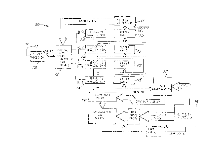
Figure 2 is a block diagram of a system 10 for displaying
off-air video pictures on a bistable display, such as a
ferroelectric liquid crystal display panel. Video information
is received at aerial 11 and demodulated by the receiver 12; it
is the~ digitized (four bits per plxel) and held in the digital
frame store 13.
To display one video frame, firstly the data is split into
four streams (one ~or each bit) and compressed by shift
registers 14 so each byte contains data for 8 pixels. The data
is then loaded into four buffer RAMs 15, so each RAM now
contains one frame of video information 1 bit deep. Accsssing
of the RAMs 15 and the frame store is done under control of the
address generator 160
: 6 ~ 5~6~
For the sequential greyscale processing the data must be
sent to the display one bit at a time, i.e. firstly all the data
from RAM O is sent to the display (the least signiflcant bit),
then followed in turn by each of the other 3 RAMs. Also, in
order to write data to the light crystal display panel each line
of data mmust be presented in a manner determined by the
multiplexing scheme; this processing is performed by the data
preparation block 17. Data is now in a form in which it can be
sent to the display panel under control of the multiplex
controller block 18, each line of data being latched into the
column drive chips 19 while rows are strobed by the row dri~e
chips 20. ThiS results in the data being latched into the
display. After a full screen of data has been written, the
backlight is flashed for a length of time corresponding to the
significance of the bit being displayed. This is done by the
lamp drive circuit 20 under control of the multiplex controller
18.
The sequence oP events which results in a full picture with
sixteen grey levels being displayed, is as follows:-
2n l. Load frame store 13;2. Load buffer RAMs 15, one significant bit to each; 3. Load data from buffer RAM O line by line into data
preparation unit 17
4. Load data from buffer RAM 1 line by line into data
preparation unit 17;
5. Load data from buffer RAM 2 line by l~ne into data
preparation unit 17;
6. Load data from buffer RAM 3 line by line into data
preparation unit 17;
7. Multiplex controller 18 sends data from data preparation
unit 17 to column drive chips 119 and controls row drive chips
20;
8. When data from RAM O has been latched into the display
(i.e. when the least significant bit for the frame is being
presented), the multiplex controller 18 signals the lamp drive
to flash for a period of time A mS;
9. Data from RAM 1 is now latched and the backlight flashed
7 : ~ ~5~ 6~:
for 2~ mS;
10. Data from RAM 2 is now latched and the baclcligh~ flashed
for 4A mS:
llo Data rrom RAM 3 is now latched and the baclclight flashed
for 8A mS;
12. The picture has now been displayed.
Assuming a frame time of 40 mS, then if it takes T mS to set up
the display 4T + 15A = 40mS.
Figure 3 shows an arrangement of metallisation patterns for
a liquid crystal display panel to achieve a two-blt greyscale,
for use additionally or alternatively to the greyscale
processing of Figures 1 and 2. On the substrate 30 having the
column electrodes, the ITO metallisation patterns are such that
each pixel has two sections 31, 32 which can be separately
driven from appropriate drive chips tnot shown) on flexible pcb
boards 33 and 34 via lines 35 and 36 respectively. For each
plxel, section 31 corresponds to the least-significant-bit, and
section 32 to the most-significant-bit. The row electrodes are
formed by ITO metallisation strips 37 on substrate 38, which can
be strobed by row drive chips (not shown) on flexible pcb 39 via
lines 40. In Figure 3, on the left hand side the substrate has
been omitted as indicated by the broken-cha$n line yet the
column metallisation is shown overlying the row metallisation,
for the purpose of simplicity.