Note: Descriptions are shown in the official language in which they were submitted.
~2~ ;~3
- 1 - llME00113
ELECTRONIC WATTHOUR METER WITH UP AND DOWN
INTEGRATION FOR ERROR CORRECTION
BACKGROUND OF THE INVENTION
The present invention relates to electronic
energy consumption metering and, more particularly, to
electronic metering of electric energy consumption in
which the direction of integration is periodically
reversed in order to cancel out offset errors.
Metering of electric energy consumption
employs measurements of electric current and voltage
fed to a load and multiplication of the measured
quantities to determine the instantaneous power
usage. The multiplied values are integrated over time
in a register to record the energy consumed.
Electro-mechanical watthour or kilowatthour meters
conventionally employ a conductive disk rotated as the
rotor of a small induction motor by the interaction of
flux fields from both a voltage stator connected
across the energy supply and a current stator
connected in series with the load. The rotations of
the disk are integrated in a geared mechanism for
recording the energy used.
Electro-mechanical watthour meters require
precision manufacture which limits the amount by which
their cost can be reduced. In addition, electro-
-~ ~z~
- 2 - llME00113
mechanical devices are inherently less reliable than
devices having no moving parts.
In my prior U.S. Patents 3,955,138, issued
May 4, 1976; 4,066,960, issued January 3, 1978;
4,485,343, issued November 17, 1984 and 4,495,343,
issued November 22, 1985, I disclose techniques for
electronic energy consumption metering which employ
time-division or amplitude-markspace modulation for
multiplying an analog variable related to
instantaneous current by an analog variable related to
instantaneous voltage. The multiplied resulting
signal contains a DC component, representing the
desired power measurement, and an AC component which
is removed by filtering. The DC component is
integrated until the integrated value attains a
threshold, at which time a change of state in the
output of the metering device indicates that the
consumption of a predetermined quantum of electric
energy has occurred.
The multiplication of the two analog
variables is achieved by alternately switching the
polarity of one of the analog variables in response to
a control signal which is pulse-width modulated by the
other analog variable. The result is a pulse train
whose height :is responsive to one of the variables and
whose instantaneous pulse width is responsive to the
other analog variable. Accordingly, the average or ~C
component of the resultant width and amplitude
modulated pulse train is proportional to power
consumption.
The pulse-width modulator in each of the
foregoing patents employs a comparator for measuring
the time at which the voltage signal passes a
predetermined reference voltage. Thus, the accuracy
with which the pulse width is controlled is dependent
Si3G~3
- 3 - llME00113
upon the accuracy of the reference voltage. In
addition, each of these prior devices requires that at
least one of the analog signals be a balanced,
double-ended signal. A balanced, double-ended signal
is conveniently generated using a center-tapped
transformer. Such a center-tapped transformer is
expensive and its elimination is thus desirable.
Furthermore, it is desirable to reduce the amount of
power consumed by the metering equipment. This
indicates that solid state devices, and preferably
low-power-consumption, solid state devices should be
used. One desirable type of solid state device
presently available is a complimentary metal oxide
semiconductor (CMOS). The circuits of the
above-referenced U.S. patents are not efficiently
implemented in CMOS technology.
OBJECTS AND SUMMARY OF THE INVENTION
Accordingly, it is an object of the
invention to provide an electronic metering apparatus
which overcomes the drawbacks of the prior art.
It is a further object of the invention to
provide an electronic metering apparatus which
requires single-ended signals for both its current and
voltage analog variables.
It is a still further object of the
invention to provide an electronic metering apparatus
which employs varying integration times for
controlling the pulse-width ratio of a constant-
frequency oscillator.
It is a still further object of the
invention to provide a pulse-width modulator for an
electric meter which produces a substantially
constant-frequency pulsed signal having a ratio of
positive to negative portions dependent upon the
amplitude of a current signal.
~2~3~9
- 4 - llME00113
Briefly stated, the present invention
provides an electronic watthour meter employing a
first analog signal representing either a load current
or voltage to pulse-width-modulate a second analog
signal representing the other of the load current or
voltage. The resulting signal contains a DC component
proportional to the product of current and voltage.
AC components are removed from the product signal in
an integrator before applying the DC component to a
threshold circuit. The threshold circuit alternates
its output between positive and negative values each
time the DC component of the product signal passes
through a predetermined positive and negative value.
Each cycle of this pulsed signal is indicative of the
consumption of a predetermined quantum of electric
energy. The pulsed signal is transmitted to a
register for integrating the energy usage. A
pulse-width modulator produces a constant-frequency
pulsed output whose positive and negative alternations
have lengths which differ in proportion to the line
signal it receives. At each alternation of the pulsed
signal, the output of the pulse-width modulator
alternates between a direct and an inverted signal.
Thus, integration is driven in alternate directions,
whereby offset voltages of active circuits are
balanced out.
According to an embodiment of the invention,
there is provided an electronic meter for measuring
energy consumption in an electrical system comprising
means for generating a first analog current signal
responsive to a current in the system, means for
generating a second analog current signal responsive
to a voltage in the system, a pulse-width modulator
responsive to one of the first and second analog
current signals for producing a first substantially
3~
- 5 - llME00113
constant-frequency, pulse-width-modulated signal
having a ratio of positive to negative portions
related to an amplitude of the one of the first and
second analog current signals, an integrator, a first
switch effective, when energized, to connect the other
of the first and second analog current signals to the
integrator, means for energizing the first switch
during one of the positive and negative portions and
for deenergizing the first switch during the other of
the positive and negative portions, whereby an output
of the first switch includes a product of the first
and second analog current signals and an output of the
integrator includes an average component of the
product, a threshold circuit, the threshold circuit
including means for changing between first and second
conditions of its output each time an output of the
integrator attains a first predetermined positive
value and a second predetermined negative value, means
for generating a complement of the substantially
constant-frequency, pulse-width-modulated signal
having a ratio of positive to negative portions
inversely related to an amplitude of the one of the
first and second analog current signals, a second
switch, the second switch includi.ng means responsive
to the first condition of the output of the threshold
circuit for applying the pulse-width-modulated signal
to the first switch, and further responsive to the
second condition of the output of the threshold
circuit for applying the complement to the first
switch, whereby the integrator alternately integrates
in a positive and a negative direction, and the first
and second conditions of the output of the threshold
circuit being indicative of a predetermined quantum of
energy consumption in the system.
Accordingly to a feature of the invention,
3~3
- 6 - llME00113
there is provided apparatus for producing a
pulse-width-modulated signal in response to a current
signal related to a current or a voltage in an
electric system comprising a signal generator, the
signal generator including means for producing a
signal voltage proportional to the current or voltage,
a series resistor in series with the signal voltage
effective for converting the signal voltage into a
first current signal, an integrator, the integrator
including an operational amplifier with an integrating
capacitor connected between an output and a first
input thereof, whereby a gain in the operational
amplifier is effective to produce a virtual ground at
an input of the integrator, the series resistor being
connected to the virtual ground, the operational
amplifier having a first input receiving an output of
the integrator, a first bi-polarity trigger receiving
the output of the operational amplifier, a resistive
voltage divider on an output of the first bi-polarity
trigger, a junction of the resistive voltage divider
being connected to a second input of the operational
amplifier, whereby a positive and a negative voltage
at the junction provides first and second threshold
voltages for the operational amplifier, a second
inverting bi-polarity trigger receiving the output of
the first bi-polarity trigger, a resistor receiving an
output voltage from the inverting bi-polarity trigger
and effective to convert the output voltage to a
second current signal, and means for connecting the
second current signal to the virtual ground whereby an
integration rate in the integrator is increased or
decreased in proportion to an amplitude of the first
current signal and a pulse-width-modulated signal is
produced.
The above, and other objects, features and
- 7 - llME00113
advantages of the present invention will become
apparent from the following description read in
conjunction with the accompanying drawings, in which
like reference numerals designate the same elements.
BRIEF DESCRIPTION OF THE DRAWINGS
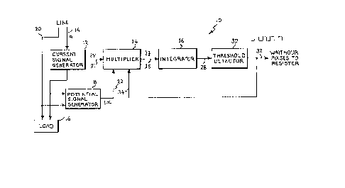
Fig. 1 is a simplified block diagram of an
electronic watthour metering circuit according to an
embodiment of the invention.
Fig. 2 is a block diagram of a multiplier of
the electronic watthour metering clrcuit of Fig. 1.
Fig. 3 is a detailed schematic and block
diagram of the electronic watthour metering circuit of
Fig. 1.
Figs. 4A-4F are curves to which reference
will be made in explaining the operation of the
invention.
DETAILED DESCRIPTION OF THE PREFERRED EMBODIMENT
Referring to Fig. 1, there is shown,
generally at 10, an electronic watthour metering
circuit according to an embodiment of the invention.
A current signal generator 12 produces an analog
current signal iy in response to a current A on a line
14 being consumed by a load 16. A potential signal
generator 18 produces an analog potential signal ix in
response to a voltage existing between line 14 and a
line 20 connec:ted to load 16.
Current signal iy and potential signal ix
are connected on lines 21 and 22, respectively, to
inputs of a multiplier 24. Multiplier 24 pulse-
width-modulates one of its two inputs in a width ratio
dependent upon the other of its inputs. For example,
the eurrent signal iy may be pulse-width modulated in
response to the amplitude of the potential signal ix,
or viee versa. The resulting produet signal iz,
containing both AC and DC components, is fed on a line
~53~
- 8 - llME00113
25 to a integrator 26. The DC component containing
the information regarding power consumption is
integrated in integrator 26 to remove the AC component
and the result is passed on a line 28 to a threshold
circuit 30.
Threshold circuit 30 detects the slowly
varying DC signal from integrator 26, first in one
direction, and then in the other direction,
continually reversing the direction of integration
when a predetermined positive and negative threshold
is reached. During upward and downward integration, a
positive or negative output pulse is applied to an
output line 32. If the positive and negative
thresholds are equal and if multiplier 24, integrator
26 and threshold circuit 30 exhibit no offset voltage
(i.e. a non-zero output voltage or current in response
to a zero input voltage or current), each cycle of
positive and negative pulses of the output signal on
output line 32 would be an accurate indication of the
consumption of a predetermined quantum of electricity
such as, for example, a watthour or kilowatthour.
When accumulated, or counted, in a register (not
shown), the energy consumed is made available for
billing or other purposes.
It is a fact, however, that active
electronic circuits do exhibit oEfset voltages. In
order to overcome such offset voltage, some of my
aforementioned U.S. patents, as well as the present
invention, integrate first in one direction, and then
in the other direction. Any errors produced by offset
voltages while integrating in one direction are
counterbalanced by equal and opposite errors while
integrating in the opposite direction. In order to
accomplish such bi-directional integration, my
aforementioned U.S. patents required comparatively
3~g
- 9 - llME00113
complex electronic switching devices, as well as at
least one center-tapped transformer in their
counterpart of current signal generator 12 or
potential signal generator 18. Such complexity adds
undesirably to the cost of the device.
A sample of the output signal on output line
32 is fed back on a feedback line 34 to multiplier
24. For a given condition of power consumption,
multiplier 24 produces a product signal iz having a
positive DC component during one condition of the
output signal fed back on feedback line 34 and a
product signal iz having a negative DC component
during the other condition of the output signal. In
this manner, integrator 26 is forced to integrate
first in one direction until the first predetermined
threshold in threshold circuit 30 is attained, and
then in the opposite direction until the second
predetermined threshold in threshold circuit 30 is
attained. Thus, offset errors are cancelled.
Referring now to Fig. 2, it should be noted
that the current and voltage signals iy and ix are
interchangeable. Thus, analog current signal iy (or
potential signal ix) on line 20 is connected to a
switch 36 in multiplier 24. Analog potential signal
ix (or current signal iy) on line 22 is connected to a
pulse-width modulator 38. Pulse-width modulator 38
produces a direct output Q on a first line 40 and an
inverted output QBAR on a second line 42. The direct
and inverted outputs of pulse-width modulator 38 are
applied to an inverting switch 43. During one
condition of the output pulses fed back on feedback
line 34, inverting switch 43 uses the direct output Q
of pulse-width modulator 38 for controlling switch 36,
whereas during the other condition of the output
signal, inverting switch 43 uses the inverted output
~2~ &~
- 10 - llME00113
of QBAR pulse-width modulator 38 for controlling
switch 36.
Referring now to Fig. 3, current signal
generator 12 includes a current transformer 44 having
a primary winding 46 connected in series with a load
current IL. A voltage Vy, proportional to the load
current, is induced in a secondary winding 48. A
loading resistor 50, of low resistance compared to the
impedance of the downstream circuits, is connected
across secondary winding 48. The resistance of
loading resistor 50, which may be, for example, about
50 to 100 ohms, controls the value of the voltage Vy
independently of changes in the impedances of the
downstream circuits. A full development of the theory
and benefits of loading resistor 50 are contained in
my aforementioned U.S. Patent No. 3,955,138.
A series resistor 52 generates current
signal iy which is connected to one terminal of switch
36. Series resistor 52 forms the effective load in
parallel with loading resistor 50, and its resistance
is therefore chosen to be substantially larger than
the resistance of loading resistor 50. Oppositely
poled diodes 54 and 56 protect against voltage spikes.
Switch 36 includes a single-pole,
single-throw switch receiving the current slgnal iy at
its input, and connecting the product signal lz to
line 25 at its output. The open and closed condition
of switch 36 is controlled by a control signal on a
control line 58. The production of the control signal
will be detailed hereinafter.
Integrator 26 contains an operational
amplifier 60 having an integrating capacitor 62
connected between its input and output. As is well
known, the high gain of operational amplifier 60
forces it to produce a signal on line 28 having a
- 11 - llME00113
sufficient voltage which, when reflected back through
integrating capacitor 62, places a virtual ground
condition at its input. As a consequence, the current
signal iy is equal to vy/R52.
The rate at which the output voltage of
operational amplifier 60 can increase is controlled by
the average value of the product signal iz fed
thereto. Thus, the slope of the signal on line 28 fed
to threshold circuit 30 depends on the average value
of the product signal iz.
Threshold circuit 30 contains a comparator
64 and a bi-polarity trigger 66 with resistors 68 and
70 connected in series from the output of bi-polarity
trigger 66 to ground. A reference voltage VR is
connected from the junction of resistors 68 and 70 to
a second input of comparator 64. Bi-polarity trigger
66 receives a positive reference voltage +VB and a
negative reference voltage -VB. In response to an
input signal even slightly positive, the output of
bi-polarity trigger 66 almost immediately switches to
-VB less a small voltage drop in bi-polarity trigger
66. Similarly, in response to an input signal even
slightly negative, the output of bi-polarity trigger
66 switches to +VB less a slight voltage drop in
bi-polarity trigger 66. At the ~unction of resistors
68 and 70, the voltage swinys between
VA(R70/(R68+R70)). For convenience, if R68 = R70,
then the voltage at the junction of resistors 68 and
70 swings between VA/2 and -VA/2. When the signal on
line 28 passes through VA2 in the positive-going
direction, or through -VA/2 in the negative-going
direction, comparator 64 reverses its output polarity
and thus reverses the output polarity of bi-polarity
trigger 66. In this manner, the output on output line
32 alternates between +VB and -VB.
3~
- 12 - llME00113
Potential signal generator 18 includes a
potential transformer 72 having a primary winding 74
connected across lines 14 and 20 and a secondary
winding 76 having a first end connected to ground and
a second end connected to a series resistor 78.
Oppositely poled diodes 80 and 82 are connected from
the downstream end of series resistor 78 to ground for
circuit protection.
Pulse-width modulator 38 includes an
integrator 84 consisting of an operational amplifier
86 and an integrating capacitor 88 connected between
the output and the input thereof. Due to the high
gain of operational amplifier 86, the signal VA2 of
operational amplifier 86 rises to a value which, when
reflected to its input through integrating capacitor
88, is effective to place a virtual ground at the
input to integrator 84. The rate at which the output
voltage of integrator 84 changes is determined by the
current available at its input. Two sources of such
current are available, as will be described.
A threshold circuit 90 contains a comparator
92 receiving signal VA2 at a first input thereof. A
bi-polarity trigger 94 receives the output of
comparator 92. Resistors 96 and 98 are connected in
series from the direct output Q of inverting switch 43
to ground with a voltage -r/-VR at the junction of
resistor 96 and 98 connected back to a second input of
comparator 92. If R96 = R98, then VR varies between +
and -VB/2. The direct output Q of threshold circuit
90 which varies between approximately +VB and -VB is
connected to the input of an inverting bi-polarity
trigger 100 which produces the inverted output QBAR
having opposite polarity to the direct output Q. The
inverted output QBAR is connected through a resistor
102 to a summing point 104 at the input of integrator
- 13 - llME00113
84. The direct output Q and inverted output QBAR of
pulse-width modulator 38 are connected on lines 40 and
42 to terminals of inverting switch 43. The output
signal fed back on feedback line 34 alternately
switches between the direct output Q and inverted
output QBAR for connection to control line 58 on each
half cycle of the output signal.
Summing point 104 is maintained at virtual
ground at all times by the voltage fed back from the
output of operational amplifier 86 to its input
through integrating capacitor 88. Thus, the voltage
at summing point 104 remains extremely close to zero
regardless of the voltage at the upstream ends of
series resistor 78 and resistor 102. Thus, the
currents through these resistors is controlled solely
by the voltages at their upstream ends and by the
values of the two resistances. As a consequence, the
current passing through series resistor 78 into
summing point 104 is independent of the current
passing through resistor 102, and vice versa. The
total current fed to integrator 84, which controls the
rate at which the output voltage of operational
amplifier 86 changes, is the super position of the two
currents (Vx/R78) ~ (QBAR/R102).
The polarity of the inverted output signal
QBAR reverses each time the signal VA2 of integrator
84 reaches +-VR/2 (assuming that R96 = R98).
If zero voltage exists between lines 14 and
20, the potential signal ix is zero. Thus, the
current at summing point 104 is equal to QBAR which
alternates between +VB and -VB. Given that
-~VB = -(-VB), then the upward and downward integration
times in integrator 84 should be substantially equal
and direct output signal Q and inverted output signal
QBAR should be symmetrical with a period T. These
3~
- 14 - llME00113
relationships are illustrated in Figs. 4A and 4B.
When the potential signal ix is not zero,
but instead varies as indicated in Fig. 4C, the
current at summing point 104 is not wholly determined
by the current fed back through resistor 102, but
instead, is the summation of currents through resistor
102 and series resistor 78. During a positive half
cycle of the potential signal ix, the total current
fed to summing point 104 is increased by an amount
Vx/R78. As a consequence, during a positive
alternation of potential signal ix, the rate at which
signal VA2 of integrator 84 changes in the upward
direction is proportionately increased and the rate at
which it changes in the downward direction is
proportionately decreased. This is illustrated in
Fig. 4D wherein the slopes of the positive-going
portions of the signal VA2 are steeper than the
negative-going portions.
During the illustrated negative half cycle
of potential signal ix, the opposite integration
speeds occur. That is, the potential signal current
subtracts from positive alternations of the signal fed
to summing point 104 through resistor 102 and adds in
the negative direction during negative alternations of
the signal through resistor 102. As a consequence,
the pulse widths of the signals Q and QBAR during a
particular portion of a positive half cycle of the
potential signal ix are the inverses of the pulse
widths during corresponding portions of the negative
half cycle. As shown in Fig. 4E, a negative cycle 106
during the positive half cycle of potential signal ix
(Fig. 4C) has the same width as a positive cycle 108
during a corresponding time in the negative half cycle
of potential signal ix.
The steepening of the slopes of the
~Z~3~
- 15 - llME00113
positive-going portions of the signal VA2 by a
positive potential signal ix is equalled by the
shallowing of the slopes of the negative-going
portions of the signal VA2 by the same positive
potential signal ix. As a consequence, the total
period T remains constant. However, the different
slopes of signal VA2 during positive-going and
negative-going integration cause the threshold values
in comparator 92 to be reached earlier or later. As a
consequence, threshold circuit 90 switches its output
between positive and negative values at times which
are advanced or retarded in proportion to the value of
potential signal ix.
Although Figs. 4A-4E illustrate only a few
cycles of signals Q and QBAR during a cycle of the
potential signal ix, in fact, a much larger number of
cycles of Q and QBAR per cycle of potential signal ix
is preferred. In the preferred embodiment, with a
line frequency of about 60 Hz, a frequency of about 5
KHz is preferred for Q and QBAR.
Referring now also to Fig. 3, when, for
example, the QBAR signal controls switch 36, product
signal iz appears as shown in Fig. 4F. Positive
alternations of the QBAR signal, which are effective
to close switch 36, have a higher duty cycle during
positive half cycles of the potential and current
signals ix and iy, respectively, than they do during
the negative half cycles of these signals. Thus, a
positive DC component, indicated by a dashed line 110,
exists in the product signal iz at this time. As a
consequence, integrator 26 integrates in the
negative-going direction until its output voltage
reaches -VR. Then, the output of threshold circuit 30
changes polarity thus producing an alternation of the
output signal on output line 32, and also reverses
~25~5i3&9
- 16 - llME00113
inverting switch 43, whereby inverted output QBAR is
removed from control of switch 36 and the direct
output Q is substituted therefore. Since switch 36 is
now controlled by the complement of the signal
previously employed, the DC component of the product
signal is equal to the negative of the DC component
illustrated in Fig. 4E. Thus, integrator 26 begins to
integrate in the upward direction until the reference
voltage +VR is attained. Then the output voltage of
threshold circuit 30 is again switched and the cycle
is repeated.
The watthour pulses on output line 32 occur
at a relatively low frequency compared to either the
line frequency or the frequency of Q and QBAR.
Although their frequency depends on the instantaneous
power consumption, a frequency on the order of, for
example, from a fraction of a Hz to a few Hz may be
expected. Thus, many cycles of the line frequency are
processed for each watthour cycle.
To minimize the sensitivity of electronic
watthour metering circuit 10 variations in reference
voltages +-VB, the resistance of resistor 102 is
preferably made equal to the resistances of resistors
96 and 98. Due to the low power consumption of CMOS
circuits, from which the preferred embodiment is
constructed, a low-cost, high-accuracy reference power
supply (not shown) may be operated using, for example,
power taken in parallel with potential transformer 72.
Electronic watthour metering circuit 10 may
be constructed in any desired manner. The invention
is, however, conceived for easy integration onto a
single chip, and such is considered to be the most
preferred embodiment.
Although electronic watthour metering
circuit 10 is described in the environment of a
~LZ~3~3~
- 17 - llME00113
single-phase power system, it would be clear to one
skilled in the art that metering of a polyphase power
system can be performed with additional apparatus
corresponding to that disclosed above. The
relationship between single-phase and three-phase
electronic power metering can be seen in a comparison
of my prior U.S. Patent Nos. 3,875,508 (single phase)
and 3,875,509 (corresponding the phase), both issued
April l, 1975.
Having described preferred embodiments of
the invention with reference to the accompanying
drawings, it is to be understood that the invention is
not limited to those precise embodiments, and that
various changes and modifications may be effected
therein by one skilled in the art without departing
from the scope or spirit of the invention as defined
in the appended claims.