Note: Descriptions are shown in the official language in which they were submitted.
~ ~t~
-- 1 --
OPTICAL SHUFFLE ARRANGEMENT
Background of the Invention
Our invention relates to processing systems
and more particularly to parallel processing systems
using data shuffling arrangements. In large scale
communication systems, switching functions adapted to
accommodate wide band information require complex
sorting operations in order to interconnect large
numbers of subscribers. Similarly, many data processing
systems need complex arrangements to perform functions
such as fast Fourier transforms, polynomial evaluation,
data sorting, and matrix manipulation. Many of these
data processing operations may be accomplished by
shuffling data elements in accordance with well-known
algorithms.
The article, "Parallel Processing with the
Perfect Shuffle," by Harold S. Stone appearing in the
IEEE Transactions on Computers, February 1971, pp. 153-
161, describes the application of the well-known perfect
shuffle technique to such data arocessing and switching
problems. U. S. Patent 4,161,036 discloses random and
sequential accessing techniques in dynamic memories
utilizing shuffling operations. The perfect shuffle
technique is well adapted to perform many switching and
data processing functions, and high density logic
circuits are available for its implementation. The
complex interconnections required for electrical
implementation of the shuffling process, however, are
difficult to achieve using prior art arrangements. The
article, "Optical Interconnections for VLSI Systems," by
Joseph W. Goodman et al appearing in Proceedings of the
IEEE, Vol. 72, No. 7, July 1984, pp. 850-866, discloses
various optical interconnections between density
""'
- 2 ~ 54`~8
integrated circuit chips which permit electrical circuit
elements to perform large scale parallel processing
involving rearrangement of information elements such as
the perfect shuffle.
Optical systems performing data processing
functions are well known in the art.
U. S. Patent 3,872,293, discloseæ a multi-dimensional
Fourier transform optical processor.
U. S. Patent 3,944,820, discloses a high speed optical
matrix multiplier system using analog processing
techniques. U. S. Patent 4,187,000, describes an analog
addressable optical computer and filter arrangement.
These patents rely on analog computation and are not
applicable to processing of information based on perfect
shuffle principles. U. S. Patent 4,418,394, discloses
an optical residue arithmetic computer having a
programmable computation module in which optical paths
are determined by electrical fields. It is an object of
the invention to provide an improved optical shuffling
arrangement adapted to perform optical parallel
processing of digital information.
Summary of the Invention
The invention is directed to an optical
arrangement adapted to rearrange elements of a multi-
dimensional array in which an element array is projected
via a plurality of optical paths. Each optical path
provides a relative shift in its projection of the
element array whereby a prescribed permutation of
- elements is obtained.
According to one aspect of the invention, a
perfect shuffle of elements is implemented by imaging a
two-dimensional element matrix on a plane with a
-
,
magnification factor of two by means of a beam splitter and
mirrors tilted to shift one image with respect to the other.
In accordance with one aspect of the invention there
is provided an optical information switching arrangement for
rearranging an applied ordered array of information-bearing
light beams comprising: means for receiving an array of
information-bearing light beams; means for directing said
light beams along a plurality of optical paths and for
projecting at most two images of the ordered array of
information-bearing light beams that travel along said optical
paths onto a preselected overlap area of said means for
receiving; means for adjusting the optical paths relative to
each other to rearrange the order of said projected
information of said two images to form a perfect shuffle of
said ordered array of information-bearing light beams within
said overlap area; and means for accepting said perfect
shuffle rearranged information in said overlap area.
In accordance with another aspect of the invention
there is provided an apparatus for optically transforming
information comprising: at least one array of information
elements; a plurality of optical paths for projecting said
array of information elements; means for shifting the optical
- paths relative to each other to rearrange the projected
information elements of the array; means for receiving
optically distinguishable information elements: and wherein:
said array of information elements comprises a planar array of
optically distinguishable information elements; said plurality
of optical paths comprises at least first and second optical
paths for projecting information elements from said array to
said receiving means; said first optical path including means
for transferring a set of said optically distinguishable
information elements to said receiving means along a first
distinct path; said second optical path including means for
transferring a set of optically distinguishable information
elements along a second distinct path shifted relative to said
'' ~,
: -
9~
3a
first distinct path to said receiving means; and the shiftingof said second distinct path relative to said first distinct
path being selected to permute the optically distinguishable
information elements at said receiving means with respect to
said array.
Brief Description of the Drawinq
FIG. 1 is a simplified illustration of the perfect
shuffle operation;
FIG. 2 depicts one optical arrangement illustrative
of the invention to perform the perfect shuffle;
FIG. 3 shows the rearrangement of information
elements performed by the apparatus of FIG. l;
FIG. 4 depicts another optical arrangement
illustrative of the invention to perform perfect shuffling
without splitting information bearing light beams;
FIG. 5 shows yet another optical arrangement
illustrative of the invention in which the information bearing
light beams are of the same length;
FIG. 6 illustrates a switching arrangement utilizing
perfect shuffle interconnection arrangements;
FIG. 7 shows an optical switching system in which
the shuffle arrangements of FIG. 5 are incorporated; and
FIG. 8 shows another optical switching circuit in
which the shuffle circuit of FIG. 5 is used.
~5 Detailed Descri~tion
The perfect shuffle is an interconnection
arrangement in which a set of informational elements E0, El,
... E7 is rearranged as a deck of cards is shuffled so that
after the shuffle the elements of the two halves of the set
alternate. FIG. 1 illustrates the rearrangement. Line 101
shows the initial set of elements in ascending order. Line
105 shows the shuffled element set. The positions of elements
E0 and E7 are unaltered. Element E4 is shifted from the fifth
position in the original set to the second position in the
shuffle set. Element El is shifted from the second
, ....................... .
.
-- 4 --
position of the original set to the third position of
the shuffled set. The other elements are rearranged as
indicated so that the first half of the shuffled set is
interleaved with the second half of the set. Where i is
S the element position, the perfect shuffle mapping may be
expressed as
P(i) = 2i for 0 < =i < = M/2 - 1
P(i) = 2i + 1 - N for N/2 < =i < -N - 1 (1)
In binary representation shuffling may be accomplished
by cyclical rotation of the bit pattern of the element
addresses in electronic circuits well known in the
art. In accordance with the invention, the shuffling
operations illustrated in FIG. 1 are carried out in an
optical arrangement in a simpler manner at substantially
higher speed.
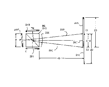
FIG. 2 shows an optical perfect shuffle device
illustrative of the invention. ~he device comprises
source element plane 201, cubic beam splitter 215,
mirrors 205 and 210, lens 220, and superimposed image
planes 235 and 240. Source element plane 201 has a
two-dimensional binary bit array thereon. Each binary
one element may be derived from a'location on a plate
that is transparent to a light beam, and each binary
2S zero element may be derived from a location on the plate
that is opaque to said light beam.
Light passing through plate 201 enters beam
splitter 215 which causes a portion of the beam to pass
.
therethrough to mirror 210 and a portion of the beam to
be deflected to mirror 205. Mirror 205 is set at an
angle so that the beam portion reflected therefrom is
deflected above optical axis 260 of the beam splitter.
~- Mirror 210 is set at an angle whereby the beam portion
therefrom is deflected below the beam splitter center
` 35 line. The beam portions reflected by the mirror pass
.: , ~ , ,.
p~
- 5 -
through magnifying lens 220. The magnified beam portion
reflected from mirror 205 forms an image on plane 235,
and the magnified beam portion reflected from mirror 210
forms an image on plane 240. Each of planes 235 and 240
may comprise a transparent plate, a plane of optic fiber
ends or other terminations well known in the art.
As indicated in FIG. 2, beam splitter 215 has
a predetermined width D and the distance between beam
splitter end 217 and image planes 235 and 240 is
4D. Each image plane has a width of 2D and lens 220 is
selected so that the magnified image on plate 235 as
well as the magnified image on plate 240 is 2D and the
images of the elements from source plate 205 are
doubled. By selecting the tilt angles of mirrors 205
and 210 to be approximately 2.9 degrees, the overlapping
sections of image planes 235 and 240 contain an image of
the elements in shuffled order.
FIG. 3 shows a view of overlapped image
plates 235 and 240 with the elements appearing thereon
identified. In the overlapped portion the sequence of
elements is E0, E4, El, E5, E2, E6, E3 and E7
corresponding to the perfect shuffling order. The
shuffled order element overlapping region may be further
processed optically or detected by arrangements well
known in the art. The nonoverlapping portions may be
discarded.
As is readily seen from FIG. 2, the
arrangement therein may be used to perform a parallel
perfect shuffle of a two-dimensional array. In general,
the arrangement is adapted to produce permutations of
information elements by interlacing shifted copies of
the input array. Such arrangements may include the
inverse perfect shuffle. The beam passing through
plane 201, however, is split so that the intensity of
the light beam for each eleme~t on the overlapping image
planes 235 and 240 is reduced. As is well known in the
art, beam splitter 215 could be a polarizing type beam
~.549~
- 6
splitter and mirrors 205 and 210 may have quarter wave
plates on surfaces facing the polarizing beam splitter
to maintain the maximum possible beam intensity.
Another arrangement to perform light beam
information permutations is shown in FIG. 4.
Advantageously, the optical configuration of FIG. 4 does
not involve beam splitting. Consequently, the light
beam intensity on the output image plane therein is only
slightly diminished by the losses in the light beam
paths. The structure of FIG. 4 comprises input
plane 401, deflecting prisms 405 and 410, Fourier
transform lens 415, deflecting prisms 420 and 425,
inverse Fourier transform lens 430 and output image
plane 435.
Input image plane 401 may comprise a plate
having spaced locations thereon. The space between
locations may be as small as 10 microns and the location
size may be as small as 4 microns. Each location may be
opaque or transparent to provide distinguishable
information. A source of at least partially coherent
light is supplied to the input plane from the left side
thereof. Alternatively, the information may be placed
on the coherent beams by other means such as light beam
logic gates so that the beams are incident on the
vertical sides of prisms 405 and 410. As shown in
FIG. 4, the information elements 1 through 8 are spaced
vertically so that the intersection of the vertices of
prisms 405 and 410 falls between the central elements 4
and 5~ ~hus elements 1 through 4 are deflected upward
by prism 405 while elements 5 through 8 are deflected
downward by prism 410.
~ he parallel beams corresponding to elements 1
through 4 are applied to the upper half of Fourier
transform lens 415. ~ens 415 is adapted to direct these
35~ beams to point 445 on the vertical side of prism 420 a
distance Fl from vertical center line 460 of the Fourier
transform lens. In similar manner, the beams for
.
- ~.
p~
-- 7 --
elements 5 through 8 are applied to the lower half of
lens 415 so that they are directed to point 450 on the
vertical side of prism 425. The vertical sides of
prisms 420 and 425 are located at distances F2 from the
vertical side of inverse Fourier lens 430 and the prisms
are operative to deflect the beams passing through
points 445 and 450 outwardly from center axis 440.
Consequently, the beams for information elements 1
through 4 are redirected by inverse Fourier lens 430 and
form parallel beams upon leaving the inverse Fourier
transform lens. These parallel beams are angled
downwardly to intersect center axis 440. The direction
of the beams for information elements 5 through 8 is
altered by inverse Fourier transform lens 430 so that
these form a set of parallel beams at an angle that
upwardly interacts center axis 440. The prism angles,
the Fourier and inverse Fourier lens, and the
distances Fl and F2 are arranged so that the information
elements at output image plane 435 are in shuffled
order 8, 4, 7, 3, 6, 2, 5, 1. For example, the wedge
angles of prisms 405 and 410 may be 10 degrees, the
wedge angles of prisms 420 and 425 may be 2 degrees,
distance Fl equal to the focal length of lens 415 and
may be 10 cm and distance F2 equal to the focal length
of lens 430 may be 10 cm. Fourier transform lens 415
and inverse Fourier lens 430 may both be of the
~achromats air spaced broad band coated lens type
produced by Spindler and Hoyer, Goettingen, Germany.
The optical arrangement of FIG. 4 provides
permutations of information elements such as the perfect
shuffle and the inverse perfect shuffle without the
splitting of information bearing light bea~s. It is
often important, however, to maintain the same light
~beam path distances for all the information element
beams. As is readily seen from FIG. 4, the path
distances for the various information element beams are
different. ~his is particularly evident when the
B
_ 8 -
element light beams are acted upon in parallel by
optical type gates such as those described in the
article, "Use of a single nonlinear Fabry-Perot etalon
as optical logic gates," by J. L. Jewell,
M. C. Rushform, and H. M. Gibbs appearing in Applied
Physics Letters, Vol. 44(2), January 15, 1984, pp. 172-
174. FIG. 5 shows yet another optical system that
features equal distance paths for all element beams.
Additionally, the relative shift between the two optical
paths is adjustable.
The optical structure of FIG. 5 includes input
image plane 501 adapted to receive information bearing
optical beams from a beam source (not shown). The beam
source may be, for exàmple, a two-dimensional array of
spaced beams arranged in a predetermined grid pattern.
At each light beam location on the grid, the beam may be
on or off to form a binary bit sequence at a femtosecond
rate. The beams are thereby modulated by information
elements. Each beam is polarized at a 45 degree angle.
After passing through plane 501, the polarized
beams, e.g. beam 570, is applied to Fourier transform
lens 505 which converts the diverging beam rays into
parallel rays impinging on polarizing beam splitter 510.
The vertical components of the polarized rays (beam 572)
pass through beam splitter 510, are reflected by
mirror 515 and are applied to inverse Fourier transform
lens 540. This inverse Fourier transform lens is
adapted to focus the rays passing therethrough at a
point 546 on output image plane 545. This path from
lens 520 to plane 545 includes path length compensating
delay 520 and polarizing beam splitter 535.
The horizontally polarized beams at input
image plane 501 are changed into parallel rays by
Fourier transform lens 505 and are deflected 90 degrees
by polarizing beam splitter 510. The deflected rays
(beam 574) impinge on mirror 525 and are redirected
therefrom to inverse Fourier transform lens 530.
- 9 -
Lens 530 is adapted to cause the parallel rays from a
particular beam to converge to a predetermined point 547
on output ima~e plane 545 after being deflected by
polarizing beam splitter 535. Lens shifter 530 to which
mirror 525 and lens 530 are rigidly connected is adapted
to move the mirror and lens combination horizontally
whereby the positions of the hori~ontally polarized
beams on output image plane 545 are shifted. The shift
in positions of these horizontally polarized beams is
precisely controlled by the position of mirror 525 to be
an integral number of array locations. This mirror
location may be adjusted to provide a shift of one or
more beam positions on output image plane 545. Such a
beam shifting arrangement according to the invention
provides perfect shuffle or other information element
rearrangements. Where the information elements for a
row at inp~t image plane 501 is El, E2, E3, E4, E5, E6,
E7, and E8 as shown in FIG. 5, adjusting the position of
mirror 525 so that the beams coming therefrom are
shifted 4.5 array locations to the right results in a
perfect shuffle order within a predetermined portion of
the output plane.
An arrangement that utilizes the perfect
shuffle technique in an interconnection network such as
the well-known Omega network described in the article,
"A Survey of Interconnection Networks," by
Robert J. McMillen appearing in the Conference Record of
the 1984 IEEE Global Telecommunications Conference,
Vol. 1, pp. 105-113, November 1984, is shown in
FIG. 6. Referring to FIG. 6, a set of 8 input optical
fiber lines are connected to optical directional coupler
switches 601-1 through 601-4 in top to bottom
order 6,1,3,4,7,2,5,0. These numbers correspond to the
destination addresses of the input lines. More
specifically, the topmost input line (0) is to be
connected to output line 6, and the bottom input line is
to be connected to output line 0 as indicated. The
.
-- 10 --
output lines from optical directional switches 630-1
through 630-4 are in top to bottom order 0,1,2,3,4,5,6,~
as indicated. For the 8 lines to ~e switched, there are
7 stages of directional coupler switches.
Each successive pair of switches in FIG. 6 is
connected through a perfect shuffle interconnection
device such as the arrangement shown and described with
respect to FIG. S. For example, switches 601-1 through
601-4 of the input stage are connected to switches 605-1
through 605-4 of the next successive switching stage
through perfect shuffle network 603. In like manner,
perfect shuffle networks 607, 612, 617, 622 and 625
interconnect the succeeding pairs of switching
stages. The perfect shuffle devices provide a regular
switching stage interconnect scheme that is particularly
important in optical networks where light beam direction
changes are limited.
The directional switches of FIG. 6 may be
electrooptic type directional couplers such as described
in the articles, "Guided-Wave Devices for Optical
Communication," by Rod C. A'ferness appearing in the
IEEE Journal of Quantum Electronics, Vol. QE-17, No. 6,
.
June 1981, and "Waveguide Electrooptic Modulators" by
Rod C. Alferness appearing in the IEEE Transactions on
Microwave Theor~ and Techni~es, Vol. MTT-30, No. 8,
August 1982. Each coupler is operative to either
connect through as indicated, for example, with respect
to coupler switch 601-4 or to crossover as indicated
with respect to coupler switch 601-1. The switching
state of each coupler switch is controlled by electrical
signals from computer device 650 in accordance with the
- required network interconnection pattern. The
arrangement of FIG. 6 may be used for packet-type
switching or for circuit-type switching, and the states
of the coupler switches will vary according to the
interconnect information supplied to device 650 on
line 642. Alternatively, optical logic devices such as
~`5~9~
disclosed in the aforementioned article by Jewell,
Rushform and Gibbs may be used as the directional
coupler switches.
FIG. 7 illustrates how the optical perfect
shuffle arrangement of FIG. 5 may be incorporated into
an interconnection network to perform the switching
operations of FIG. 6. Directional couplers 701 and 705
are shown as line array switches. It is to be
understood that the directional couplers could be of the
two-dimensional type to accommodate a two-dimensional
array of light beam elements. Mirrors 701 and 703 are
constructed to be switchable so that they may be
reflecting or transmitting as controlled by either an
electrical or an optical signal from control
processor 750. The mirrors may be of the type described
in the aforementioned article by J. Jewell et al or of
the liquid crystal light valve type described by
B. Clylmer and S. A. Collins in the article, "Optical
Computer Switching Network," appearing in Optical
Engineering, Vol. 24, No. 1 ~1985). In FIG. 7, the
input light beams in the same order as in FIG. 6 pass
through mirror 700 while it is in its transmitting
state. The light beams from mirror 700 are applied to
- directional coupler switch array 701 which is controlled
by device 750 to provide the same switching
configuration as coupler switches 601-1 through 601-4 in
FIG. 6. The light beams pass through directional
coupler switch 701 so that the order of the beams is
changed to 6,4,3,2,7,5,0 as indicated and enter perfect
shuffle unit 701. As described with respect to FIG. 5,
unit 701 is operative to interleave the light beams, and
the interleaved beams are supplied to the input of
directional coupler switch 705 in 1,2,6,7,4,5,3,0 order.
- Directional coupler 705 operates in the same manner as
coupler switches 605-1 through 605-4 in FIG. 6, and as
in FIG. 6 there is no crossover of the light
beams. Perfect shuffle unit 707 which corresponds to
;~
~ 2~ ~
- 12 -
shuffle device 607 in FIG. 6 is operative to interleave
the light beams from coupler 705 so that the order
1,4,2,5,6,3,7,0 results at its output. This order
corresponds to the output at shuffle device 607.
At this point in the operation of the circuit
of FIG. 7, mirror 700 along path 752 is switched to its
reflecting mode. Consequently, the input beams are cut
off, and the beams exiting from perfect shuffle unit 707
are reflected onto switch 701. The control signals to
coupler switches 701 and 705 are modified so that their
switching states correspond to those of coupler
switches 610-1 through 610-4 and 615-1 through 615-4,
respectively, and the circuit of FIG. 7 performs the
operations of coupler switch 610, shuffler 612, coupler
switch 615 and shuffler 617. The light beams emerging
from perfect shuffle unit 707 as a result of the first
reentrant beams therefrom are then in 1,2,4,5,3,7,6,0
order in conformance with the operation of SWitch 610,
shuffler 612, switch 615 and shuffler 617 of FIG. 6.
When the beams emerge from shuffler 707 the
second time, the states of coupler switches 701 and 705
are again modified to conform to the states of
switches 620-1 through 6?0-4 and 625-1 through 625-4,
respectively. The circuit of FIG. 7 then performs the
functions of switching stage 620, shuffler 622,
switching stage 625 and shuffler 627 of FIG. 6 so that
the light beams emerge from shuffler 707 in the same
order as those from shuffler 627 in FIG. 6. Coupler
switch 701 is then placed in the switching states sh~own
with respect to coupler switch 630, and the light beams
from shuffler 707 are passed therethrough via
mirror 700. Mirror 703 of perfect shuffler device 702
is~ placed in its transmittal mode by a signal from
control device 750, and the light beams impinging
thereon are supplied in 0,1,2,3,4,5,6,7 order to
utilization device 770. The network interconnections of
; FIG. 6 are thereby accomplished. Mirror 700 may then
''"' ,
- 13 _ ~ W~4~
receive another set of light beam information signals
which may be switched as controlled by signals from
control computer 750.
Another mode of operation is illustrated in
the circuit of FIG. 8. FIG. 8 shows a multi-level
optical switching network that performs the operations
of the circuit of FIG. 6 utilizing the perfect shuffle
device of FIG. 5. In FIG. 8, directional coupler
switches 801, 805, 810, 815, 820, 825 and 830 are
controlled by switch control processor 850. The states
of the directional couplers are the same as in FIG. 6.
For example, device 801 comprises a set of 4 directional
couplers which are equivalent to directional coupler
switches 601-1 through 601-4 in FIG. 6. The 3 left side
directional couplers of device 801 are set to their
crossover states (not indicated) as are directional
coupler switches 601-1 through 601-3, and the rightmost
coupler of device 801 is set to its direct connection
state (not indicated) as is coupler switch 601-4. A
perfect shuffler interconnects each pair of directional
coupler switches. Perfect shuffle device 803 is
interposed between directional coupler switches 801 and
80S and is extended so that it is also interposed
between directional coupler switches 810 and 815 as well
as between coupler switches 820 and 825. Perfect
shuffle device 807 is connected between coupler
switches 805 and 810, coupler switches 815 and 820, and
switches 825 and 830.
The 8 light beams incident on directional
coupler switch 801 through the slot in mirror 869 are
represented by centered single beam 800. These beams
are directed in spiral-llke fashion throùgh the network
of FIG. 8. Mirrors 860 and 869 are arranged to complete
the spiral path from the shuffle devices to the
succeeding directional coupler switch. As described
with respect to FIG. 6, the beams incoming to the
network may be in the order shown at the left side of
- 14 - ~ 4~
FIG. 6. With switch control processor 850 providing the
control signals as in FIG. 6, the beams are crossed over
or passed through the sections of directional coupler
switch 801, rearranged in perfect shuffler 803 and
S applied to directional coupler switch 805 via
mirror 860. The beam array is passed through the
shuffle and directional coupler devices placed so that
the beams follow a downward spiral-like path through the
network devices and emerge from coupler switch 830 as
beam 809. Output beam 809 is representative of 8 beams
which are ordered as indicated at the outputs of
switches 630-1 through 630-4 in FIG. 6. As described
with respect to FIG. 6, the directional coupler switches
of FIG. 8 may be replaced by optical logic devices, and
the control arrangements may be used for packets where
the address information is contained in a packet header.
Advantageously, the network may extend to a large number
of lines, and the optical switching may be accomplished
in the order of femtoseconds.
The invention has been illustrated and
described with reference to particular embodiments
thereof. It is to be understood, however, that various
changes and modifications may be made by those skilled
in the art without departing from the spirit and scope
of the invention.
,: