Note: Descriptions are shown in the official language in which they were submitted.
3~
-- 1 --
A FABRICATION PROCESS FOR
AEIGNED AND STACRED CNOS DEVICES
Backqround of the Invention
The present invention relates to three
dimensional metal oxide semiconductor (MOS) technology
and, in particular, to vertically integrated or
"stacked CMOSFET structures.
Two of the continuing goals of the
microelectronics industry are to increase device
packing densities and to enhance performance
characteristics such as the speed of operation. The
ongoing attempts to scale devices and associated
structures have been successful to date in reducing
the size and relative spacing between active devices,
conductive paths and regions of isolating dielectric,
but with some resulting problems caused by, for
example, difficulties in photolithographic resolution
and device interaction.
Another way to increase MOS device density,
besides scaling per se, involves vertical integration,
in which devices are stacked one above the other.
This appr~ach has significant potential for increased
device packing density. In addition, in CMOS
technology, the stacked structure can eliminate
p-wells, decrease the latch-up phenomenon and provide
decreased wire routing complexity.
There are a number of approaches for
configuring such stacked MOSFETS. For example, a
separate gate, stacked CMOS configuration is described
in Rawamura et al., ~Three-Dimensional CMOS ICs
Fabricated Using Beam Recrystallizationn, IEEE
Electron Device Letters, Vol. 4, No. 10, pp. 366-368,
1983. As shown in FIG. 2, this stacked device 26
includes two ~upright~ transistors, that is, two non-
inverted PMOS and NMOS transistors 27 and 28 which
have separate gates 29 and 30 as well as separate ~T~
~.: ~534
-- 2
source-channel-drain structures 31 and 32. The lower,
PMOS device 27 is apparently formed using standard
silicon technology; then a double layer of
phosphosilicate glass (PSG) 33 and nitride 34 is
formed as the intermediate insulation layer between
the stacked devices. The function of the double
insulation layer is to minimize surface undulation and
to decrease optical reflection during laser
irradiation of the polysilieon ehannel structure 32.
Apparently, the NMOS transistor 28 is formed over the
PMOS transistor 27 by depositing a second layer of
polysilicon (gate 29 is the first poly layer), which
is recrystallized and selectively doped to form the
NMOS source-channel-drain strueture 32, then
depositing a third layer of poly and forming it into
the NMOS gate 30.
A vertically and horizontally integrated
structure is described in Gibbons et al., "Stacked
MOSFETs in a Single Film of Laser-Recrystallized
Polysilicon, n IEEE Electron Device Letters, Vol. 3,
p. 191, 1982. In this structure, two transistors are
provided in a cross-shaped single gate configuration.
The paired opposite ends of the cross form the souree
and drain of the two transistors. The upper and lower
surfaces of the polysilicon layer at the junctive of
the cross serve as the gates for the two transistors.
Stacked CMOS structures which use a single
common gate and recrystallized polysilicon for the
upper source-channel-drain structure are also
described in Chen et al., "Stacked CMOS SRAM Cell, n
IEEE Electron Deviee Letters, Vol. 4, p. 272, 1983:
and in Colinge et al., "Staeked Transistors CMOS
( ST-MOS), an NMOS Technology Modified to CMOS,~ IEEE
Transactions on Electron Deviees, Vol. ED-29, No. 4,
pp. 585-589, April 1982. Colinge et al. discloses a
stacked, common gate CMOS inverter which comprises a
conventional lower field effect transistor and an
~c~ 5 3
-- 3 --
upper PMOS field effect transistor. Colinge et al.
uses standard poly NMOS processing to form the lower
device. That is, source, drain and self-aligned gate
electrode 85 (poly I) are formed in and on the
substrate. Then there is added a selectively
implanted and laser recrystallized polycrystalline
silicon layer, which forms the PMOS source, channel
and drain. The PMOS drain contacts the NMOS drain to
provide an inverter configuration.
Reviewing the relevant part of the Colinge et
al. process in greater detail, after forming the NMOS
device, the common gate is oxidized and etched to
smooth the upper surface for the formation of the
second gate oxide. The PMOS gate oxide is then grown
on top of the common gate and the second poly layer
(poly II) is deposited and implanted to adjust the
threshold voltage of the upper PMOS device. The poly
II layer is then selectively capped with an
antireflective silicon nitride coating and is
recrystallized using a CW argon laser. Subsequently,
the poly II channel is masked and the source~drain
regions are doped p-type by boron implantation. The
ætructure is then completed by the standard sequence
of poly II patterning, oxide caping, contact cuts,
aluminum deposition and metal patterning.
It should be noted that the source-channel-
drain structure of the upper PMOS device is not self-
aligned with the common gate. Consequently, the
alignment of the p~ source-drain implant mask is
critical to minimize capacitive coupling between the
source/drain regions and the gate electrode.
Finally, Pashley U.S. Patent No. 4,272,880,
discloses a stacked, common gate MOSFET inverter in
which the source-channel-drain structure of a lower
NMOS device is formed in an epi layer and the source-
channel-drain structure of the PMOS device is formed
in a layer of recrystallized polysilicon. The totally
34
\
-- 4 --
self-aligned nonplanar process patterned nitride as an
etch mask to define the common gate, then uses the
same mask as an implant mask in forming the n-type
source and drain. Thereafter, the upper part of the
epi layer is oxidized to form an isolation layer over
the n-type source and drain with the nitride being
retained to mask an underlying gate oxide layer during
a p-type implant of the isolation oxide surface.
Subsequently, the p-type source and drain are formed
by updiffusion from the doped oxide surface so that
they are aligned with the common gate.
In short, the Pashley process uses the
nitride in accordance with standard silicon self-
alignment techniques to patterning and implanting the
lower NMOS transistor, then retains the nitride and
uses it as a dopant implant mask for the isolation
oxide surface so that the p-type source and drain are
aligned with the common gate by updiffusion.
Summarv of the Invention
In view of the above discussion, it is one
object of the present invention to extend the above-
described three dimensional stacked device technology
to provide a fully planarized, fully aligned, stacked
common gate MOSFET structure.
It is another object of the present invention
to provide a unique process sequence for fabricating
the above structure, in which the gate oxide of the
upper device and the aligned source and drain of the
upper device are defined during the process of
planarizing the interlevel dielectric which separates
the upper and lower devices. ~his approach eliminates
one or more masking operations and minimizes the gate
overlap or Miller capacitance in the stacked
structure.
In one aspect, the present invention relates
to a process for forming a fully aligned stacked
S5~}4
-- 5
MOSFET device pair in which the lower self-aligned
device is formed by silicon gate technology and the
aligned upper device is formed by the unique
fabrication sequence of defining doped regions at the
sides of the common gate electrode by the process of
planarizing the interlayer dielectric between the
devices, then forming source and drain regions in the
overlying polycrystalline silicon channel layer by
updiffusion from the doped region.
In another more specific aspect, the present
invention relates to a process for forming a common
gate, stacked, totally aligned MOSFET device pair in
which the bottom NMOS FET is formed by conventional
self-aligned silicon process techniques. An
interlayer dielectric is formed between the devices
and over the common gate and contains doped regions at
the sides of the common gate. Planarizing techniques
are then applied to level the interlayer dielectric
and expose the upper surface of the gate electrode.
The gate oxide for the upper device is then
automatically grown self-aligned, that is, precisely
delineated on, the upper electrode. A polysilicon
layer is defined over the interlayer dielectric and
gate oxide structure and is recrystallized.
Recrystallization also anneals the n+ regions, such as
the NMOS source and drain. The PMOS source and drain
are then formed by updiffusion from the doped regions,
aligned with the gate electrode and gate dielectric.
In still another aspect, the present
invention is a process for forming a pair of stacked
MOSFETs having a common gate electrode and comprises:
forming an NMOS FET including source, drain and gate
electrode; depositing a first conformal undoped oxide
layer on the NMOS FET structure; depositing a second
layer of conformal oxide on the first layer, the
second layer being p-type doped and when combined with
the first layer forms regions of the second layer on
5534
opposite sides of the gate electrode; depositing a
sacrificial planarizing layer over the doped second
layer; etching the sacrificial layer and the oxide
layers at equal rates until the upper surface of the
gate electrode is exposed and defines isolated p-type
glass regions on opposite sides of the gate electrode;
selectively forming a gate oxide by oxidizing the
upper surface of the gate electrode; forming a
polysilicon layer over the doped glass regions and the
gate oxide; and heating the upper polysilicon layer to
recrystallize the polysilicon and to updiffusing
dopant from the glass layer into p-type source and
drain regions which are aligned with the common gate
electrode.
Alternatively, an oxide capping layer can be
formed over the doped second layer prior to
planarization to prevent premature outdiffusion.
Brief Description of the Drawinqs
FIG. 1 through 5 are schematic cross-
sectional illustrations of a monolithic semiconductor
integrated circuit taken sequentially during the
course of fabricating a stacked MOSFET device using
the process sequence of the present invention.
Detailed Description of the Invention
FIG. 1 illustrates the starting point for
implementing the process sequence of the present
invention. The starting structure includes a
conventional self-aligned NMOS device 100 formed in a
p-type silicon substrate 101. As is well known, one
sequence for forming the NMOS structure involves the
use of LOCOS techniques to define the thick field
oxide regions 102 which separate the active device
areas, growing the thin gate oxide 103, adjusting the
. threshold voltage of the n-channel device using a
light boron ion implantation, and depositing and
-- 7 --
delineating the gate electrode 104 (poly I).
Typically, the poly I layer is deposited to a
thickness of about 500 nanometers using low pressure
chemical vapor deposition (LPCVD), is doped using
standard in sit~ doping techniques, and is masked and
patterned to define the gate electrode 104. Then, a
second doping is carried out to form the n+-type
source and drain areas 105-105, thus doping preferably
implemented by ion implementation.
Because the gate oxide for the upper device
is to be formed on the upper surface 106 of the gate
electrode 104, the poly I layer is deposited or upper
surface is post-deposition treated to provide a
topography which is free of surface asperities and
spikes. One treatment involves oxidizing the upper
surface 106 of the polysilicon 104 by subjecting the
structure to a temperature of about l,000C in a wet
oxidizing ambient, to grow at least 20 nanometers of
oxide on the poly I and, in so doing, to consume a
surface layer of the poly I. Then, the oxide is
etched off using a conventional etchant, such as a
buffered hydrogen flouride. The as-deposited
thickness of the poly I layer may be increased to
offset the amount consumption during this oxidation
step. Typically, this surface treatment is done prior
to patterning and doping of gate 104, but can be done
after these steps if desired~
The poly I layer is next doped, masked and
etched, using conventional n~-type implant doping,
photolithographic mask formation and poly etching
techniques, to form the polysilicon gate electrode
104. The gate electrode 104 is then doped, for
example by phosphorus ion implantation with an energy
of 100 Kev and a 1.4 x 10E16 dose.
Referring next to the structure shown in FIG.
2, the initial steps of the unique process sequence
according to the present invention are implemented by
'5~3~
-- 8 --
depositing undoped CVD silicon dioxide layer 107
conformally over the NMOS structure 100, followed by
depositing a boron doped CVD silicon dioxide layer 108
conformally over layer 107. The layer 107 is the
interlayer dielectric which electrically isolates the
lower NMOS device 100 from the upper PMOS device 130
(FIG. 5). Heavily doped layer 108 serves as an
impurity source for forming the self-aligned source
and drain of upper device 130. It should be
recognized that the boron diffuses laterally as well
as vertically during the updiffusion step, thereby
closing separation 111 between the doped glass 108 and
the sidewalls 112 of gate electrode 104. Typically,
the undoped oxide layer 107 is conformally deposited
to a thickness of about 300 nanometers by LPCVD, (for
example, 300 mT; 420C; silane and oxygen system).
The doped oxide layer 108, commonly known as boron
glass, can be formed, for example, by the same process
as the layer 107, to a thickness of about 200
nanometers, and doped either during its formation, for
example by using boron-nitride as a solid diffusion
source (4BN+302-~2B203+2N2t) or by adding a gaseous
boron dopant to the LPCVD system, or afterwards. A
capping layer of undoped oxide having a thickness of
20-30 nanometers may be applied over the boron glass
layer 108 to prevent outdiffusion prior to the poly II
deposition.
To provide the aligned upper source and
drain, advantage is taken of the ~step~ which is
formed by the polysilicon gate electrode 104 relative
to the substrate surface. Because of this step and
the resulting stepped surface topography of conformal
layers 107 and 109, these layers are relatively thin
adjacent the edges of the gate electrode 104. As a
consequence, the corresponding edges 109-109 of the
doped oxide layer 108 are situated very close to the
gate edges 112-112. In short, the boron doped CVD
~2',~S~3~
g
glass layer 108 is formed closely adjacent the gate
electrode 104 so that during the subsequent formation
of the source and drain of the upper PMOS device by
updiffusion, this glass layer forms the source and
drain closely adjacent the upper gate electrode,
thereby providing alignment very similar to that
provided by conventional self-aligned silicon
technology.
Referring now to FIG. 3, the next step is to
planarize the oxide layers 107 and 108 and to expose
the upper surface 106 of the gate electrode 104. One
suitable technique involves the spin-on application of
a relatively low viscosity organic layer 114 on outer
surface 115 of oxide 108. The spun-on material is
caused to flow to a relatively smooth surface 116 by
the centrifugal force of the application or by a
subsequent low temperature bake. Reactive ion
etching, which etches the organic material and the
oxides at approximately the same rate, is then used to
clear the organic layer from the upper surface and
replicate the surface smoothness 116 of the organic
coating 114 in the resulting outer surface 117 of
layers 107 and 108. See FIG. 4.
Representative planarizing techniques
employing a spin-on photoresist deposition and a 1:1
photoresist-to-oxide etch operation are described in
U.S. Patent Nos. 4,025,411 and 4,407,851.
Referring further to FIG. 4, the
planarization process completely removes oxide layers
above the qate electrode 104 and above the field oxide
down to the level of the surface 106 of the gate
electrode 104, thereby precisely defining the boron
glass regions 118-118 in the device active area
adjacent the common gate electrode 104. The depth of
the boron qlass region 118-118, and its proximity to
gate electrode 104, can be increased or decreased as
desired by, respectively, decreasing or increasing the
~2~
-- 10 --
thickness of the underlying undoped CVD oxide layer
107. For the exemplary 300 nanometer thickness of
oxide layer 107, the 200 nanometer thickness of doped
glass layer 109, and for the 500 nanometer thickness
of the electrode 104, the boron glass dopant source
regions 118-118 are about 100-200 nanometers thick.
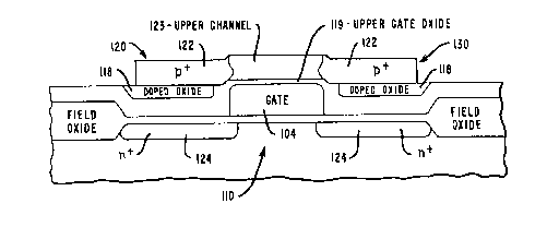
Referring now to FIG. 5, after the
planarization sequence, a gate oxide layer 119 is
selectively grown to a thickness of about 25-50
nanometers on the highly doped polysilicon, typically
by dry oxidation at approximately 900C for 40
minutes, possibly with 3% by weight of HCl. The
oxidation process proceeds much faster on the silicon
gate electrode 104 than on the surrounding oxide, with
the result that the upper gate oxide 119 is
predominantly formed on the gate electrode. Also, it
should be noted that some growth of oxide over regions
118-118 is not detrimental. In short, the gate oxide
119 is automatically formed self-aligned with the gate
and the subsequently diffused PMOS source and drain
regions.
Immediately after forming the gate oxide 119,
and to avoid contamination of that oxide, a second
polysilicon layer (poly II) is formed to a thickness
of about 250-450 nanometers, again using conventional
techniques such as LPCVD. The poly II layer is then
lightly doped by ion implantation, for example with
boron at an energy of 35 keV and a dose of lE12-2E13,
to provide the requisite channel inversion threshold
in upper channel region 123. The poly II layer is
then capped with an antireflective coating of nitride
(not sha~n) which is formed about 40-45 nanometers
thick by conventional processing such as LPC~D. Next,
the poly II layer is for example exposed to a CW argon
laser beam (backside temperature of 500C; spot size
50 micrometers; step size 15 micrometers; beam power 9
wattE; scanning speed 55 cm/sec.) to convert the
5.34
polysilicon to device-quality material comprising a
recrystallized matrix of crystallites having various
crystal orientations, and to simultaneously anneal the
n-channel source and drain regions 105-105 (~ig. 4).
This operation also redistributes the boron from doped
oxide regions 118 into selected, self-aligned regions
of the recrystallized poly II layer to form p-channel
transistor source/drain regions 122-122. The nitride
cap (not shown) is then removed using concentrated
hydroflouric acid and the recrystallized poly II layer
is patterned to the source 122 channel 123, and drain
122 configuration shown in FIG. 5.
If conventional stacked device technology
were being used, the functionally similar operation
would involve a masking of the channel, for example,
using photoresist or silicon dioxide, and an implant
of the PMOS source and drain regions. Such a process,
however, would not provide alignment between the two
stacked devices 110 and 130. In contrast, using the
present invention, the integrated circuit is subjected
to a thermal diffusion sequence, for example at
approximately 900C for 30 minutes in steam to
updiffuse boron dopant from regions 118-118 into the
poly II layer to complete the formation of the source
122 and drain 122 for the upper, p-channel transistor
in alignment with the gate electrode 104. The exact
conditions are influenced by the presence and the
thickness of any capping layer which may be formed
over boron gla~s layer 108 to inhibit premature boron
outdiffusion. This thermal drive-in also serves to
diffuse and anneal the source and drain 105-105 of the
n-channel transistor 110 to regions 124-124 as shown
in Fig. 5.
In summary, the present invention uses a
601id dopant source (regions 118-llB, FIG. 4) both (1)
to define the location of the gate oxide 119 of the
upper device 130 in alignment with the common gate
5`34
-- 12 --
104, and also (2) to form the source 122 and drain 122
of the upper device both in alignment with the upper
device 130 gate oxide and common gate 104. The result
is a completely aligned, stacked transistor device
pair which is characterized by minimum gate to upper
source and upper drain capacitance and is formed
without the usual mask alignment sensitive
photolithographic processes.
Based upon the above detailed description of
the invention, those of usual skill in the art will
readily derive alternatives within the scope of the
following claims.