Note: Descriptions are shown in the official language in which they were submitted.
3$~
IMPROVED RF DRIVER OWER SUPPLY
~ und and Field of the Invention
This invention relates to the art of regulated power
supplies for supplying RF drive to a load, such as a radio
transmitter.
Whereas the invention will be described in conjunction
with providing an RF drive for an AM transmitter~ it is to
be appreciated that the RF drive may also be utilized in an
FM transmitter for use in radio broadcasting or an FM
transmitter for the audio portion of a TV transmit~er.
It is known in the art to provide an RF drive to the
power amplifier stage in an AM transmitter. The RF drive
typically receives an RF signal from an oscillator and
amplifies the signal prior to employing it as a drive to a
~ power amplifier. The RF drive includes a plurality of
:
power amplifiers each supplied with an identical regulated
DC voItage and each serving to provide amplification of the
input RF signal. The amplified RF signals are then combined
~::
i6~17
as an RF drive to be supplied to the power amplifier stage
of the AM transmitter. Thus, the RF drive is the sum of
the outputs o~ each of the amplifiers in the driver.
In the absence ok drive regulation, the RF drive may
vary somewhat with power line voltage resulting in
variations of the regulated DC voltage supply, temperature
variations taking place within the amplifiecs in the
driver, as well as variations in the performance of the RF
oscillator. It has been known in the aet to employ complex
switching regulators or low efficiency linear regulators in
an attempt to regulate the complete RF driver.
The U.S. patent to M. Kumar et al., 4,439,744 discloses
a variable power amplifier employing a plurality of power
amplifiers, each producing a different power level.
Depending upon the total power level desired, one or more
of the amplifiers is turned on to provide the desired
output power. Each o the power amplifiers is either fully
on or fully off and there is no sampling of the output RF
drive to determine variations ~rom a desired level for use
in controlling a linear amplifier for supplying a DC
voltage of a magnitude in accordance therewith to one of
the power amplifiers or providing a regulated RF drive, as
is accomplished in accordance with the present invention.
Summary_of the Invention
~ ~ It is an object of the present invention to provide an
;~ improved RF driver power supply for supplying a regulated
6~3'7
27768-47
RF drive to a load, such as a transmitter, in such a manner to
make the RF drive independent of power line voltage variations
and thereby maintain very low transmitter distortion.
It is a still further object of the present invention
to provide a sequenced linear regulator to regulate part of the
RF drive to thereby attain a simple low cost efficient drive
regulator.
In accordance with the present invention, there is
provided an RF driver power supply for supplying a regulated
power amplified unmodulated RF drive signal to an RF modulator in
an RF transmitter, comprising: an RF oscillator for providing an
RF input signal; a DC voltage source for providing a DC voltage
V; a plurality of power amplifiers each having a first input for
receiving said input RF signal and each having a second input for
receiving a DC voltage signal and each serving to amplify said
input RF signal by an amount dependent upon the magnitude of a
said DC voltage signal supplied to the second input thereof to
provide an amplified RF signal; means for applying said input RF
signal to each said first input; means for combining said
amplified RF signals to provide a said unmodulated RF drive
signal to be applied to a said RF modulator; means for applying
said DC voltage V to the second input of at least a first one of
said power amplifiers; and regulating means for regulating the
magnitude of said unmodulated RF drive signal including means for
applying a fract.ional portion of said DC voltage V to the second
~.`.
6~7
27768-47
input oE a second one oE said power amplifiers with the
fractional portion varying as a function of any variation in the
magnitude oE said unmodulated RF drive signal with respect to a
desired magnitude thereof.
In accordance with a more limited aspect of the present
invention, the regulator includes means for sampling the
unmodulated RF drive signal and providing a sample signal having
a magnitude dependent upon that of the unmodulated RF drive
signal. A first error signal is provided having a magnitude
dependent upon the difference between the sample signal and a
first reEerence level. A first linear amplifier is coupled to
the voltage source V and responsive to the error signal for
providing a fractional portion of the voltage source in
accordance with the magnitude of the error signal for application
to the second input of a second one of the power amplifiers so as
to thereby provide a regulated RF drive signal.
srief Description of the Drawinqs
The foregoing and other objec-ts and advantages of the
present invention will become more readily apparent from the
following detailed description as taken in conjunction with the
accompanying drawings, wherein:
Fig. 1 is a schematic-block diagram of one application to
which the present invention may be applied; and
i;6~7
27768-47
Fig. 2 is a schematic-block diagram of the preferred
embodiment oE the invention.
_escri tion of a Preferred Embodiment
Reference is now made to the drawings which present a
preferred embodiment of the present invention. One
:
4a
, ~
--5--
application of the present invention is an i~proved RF
drive for an AM broadcasting transmitter operable over a
frequency band on the order of 500 to 1600 KHz. An example
of such an application is illustra~ed in Fig. 1 to which
reference is now made. This example takes the form of a
digital amplitude modulator, such as that illustrated and
described in my U.S. Patent No. 4,580,111, which issued
April 1, 1986 and which is assigned to the same assignee as
the present invention. Such a modulator is particularly
useful as a high power amplitude modulator Eor use in AM
radio or TV broadcasting.
Refesring now to Fig. 1, the amplitude modulator 10 is
illustrated as receiving an input signal from an input
source 12 which may be the source of an audio signal. The
modulator 10 provides an output RF carrier signal which is
amplitude modulated as a function of the amplitude of the
input signal from source 12. The amplitude modulated
carrier signal is provided on an output line connected to a
load 14, which may take the form of an RF transmitting
antenna. As brought in my aforesaid U.S. patent, a
digitizer 16 provides a plurality of digital control
signals Dl through DN which have values which vary in
accordance with the instantaneous level of the input
signal. The control signals are binary signals each having
a binary 1 or a binary 0 level. T,he number of signals
having binary 1 or binary 0 levels is dependent upon the
instantaneous level of the input signal.
i61~37
--6--
Each of the output control signals Dl-DN i5 supplied to
one o a plurality oE N 1~ power amplifiers P~l-PAN of
a power amplifier stage PA. The control signals serve to
turn an associated power amplifier either on or o~f. Thus,
if the control signal has a binary 1 level, then its
associated amplifier is inactive and no signal is provided
at its output. However, if the control signal is a binary
0 level, then the power amplifier is active and an
amplified carrier signal is provided as its output. Each
power ampli~ier has an input connected to a single common
RF source 20. The RF source 20 serves as the single source
of an RF carrier signal which is supplied by way of an RF
splitter 22 so that each amplifier PAl-PAN receives a
signal of like amplitude and phase and fre~uency. These
signals are supplied to a combiner circuit 24 comprised o~
a plurality of transformers Tl, T2, ~3, . . . TN.
The secondary windings act as an independent signal source
whereby the signals provided by the various transformers
additively combine with one another to produce a combined
signal which is supplied to the load 14. This combined
signal has the same frequency as the RF signal supplied by
the RF source 20, but the amplitude of the combined signal
is modulated in accordance with the input signal supplied
by the input source 12.
It is common in broadcast tran~mitters such as that
illustrated in Fig. 1 that the RF carrier signal supplied
~ .,
--7--
to the power amplifier stage PA be preamplified.
Consequently, as is shown in Fis. 1, the RF source 20
includes an RF driver 40 which is powered by a high voltage
from a DC voltage source 42 for amplifying the RF signal
obtained from an RF oscillator 44. The DC voltage source
42 may typically take the form of a regulated power supply
which converts power taken from an AC line source 46 and
converts it into regulated DC voltage, such as on the order
of 230 volts. The RF drlver 40 may have several stages
each supplied with the regulated DC voltage from source 42
for providing pre-amplification of the RF carrier signal.
In the absence of drive regulation, the output of the
~ driver may cause transmitter distortion. Thus, the
output of an unregulated driver may not be constant, but
will vary somewhat in dependence upon temperature
variations of the amplifier stages within the RF driver or
vary because o~ variations in the DC voltage supplied by
source 42 because of ~luctuations in the line voltage or
may vary somewhat because of the variations in the accuracy
of the RF oscillator 44. Prior art attempts to regulate
the RF driver have included complex switching regulators or
low efficiency linear regulators to regulate the complete
RF driver. In accordance with the present invention, there
is provided a sequenced linear regulator to regulate a part
of the driver and thus obtain a si~ple low cost efficient
drive regulator so as to make the RF drive independent of
.~
37
27768-47
power line voltage and the like, and thereby maintain very low
transmit-ter distortion.
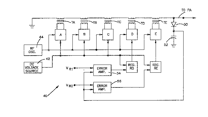
Attention is now directed to Fig. 2 which illustrates
the improved RF driver 40 in accordance with one embodiment of
the present invention. The RF driver 40 includes a plurality of
RF power amplifiers A, B, C, D and E. Each of these amplifiers
serves to amplify the RF carrier signal obtained from the RF
oscillator 44. The amplified output signals are supplied to
respective transformers TA, TB, TC, TD, and TE. The secondary
windings act as an independent signal source whereby the signals
provided by the various -transformers additively combine with one
another to produce a combined RF drive signal which is supplied
to the power amplifier stage PA of Fig. 1. It will be noted that
amplifiers A, B and C are each directly connected to the DC
voltage source 42 whereas amplifiers D and E are indirectly
connected to the voltage source by way of linear regulators RD
and RE, respectively. Each of these amplifiers A-E may take the
form of a class D MOSFET transistor amplifier. A suitable
amplifier for this purpose may take the form as illustrated in
Fig. 2 of my aforesaid U.S. Patent No. 4,580,111. Such an
amplifier includes MOSFET transistors which effectively act as
switches and are preferably connected in a bridge circuit. The
amplifiers A, B and C are constantly turned on and operate in a
;~ ,, . ~
;6~
g
saturated state. This amplifies the RF input signal by a
fixed amount, the magnitude of the output signal being
dependent upon that oE the DC voltage source 92.
Consequently, the outputs obtained from the amplifiers A, B
and C are equal and are combined by means of transformers
TA, TB and TC.
In accordance with the present invention, power
amplfiers D and E are constructed the same as amplifiers A,
B and C and each serves to amplify the RF input signal
obtained from oscillator 44. Whereas amplifiers D and E
are also class D amplifiers that operate in saturation in
the manner of a switch, the magnitude of the output signals
derived therefrom are limited in dependence upon the
regulated DC voltage obtained from regulators RD and RE,
respectively, in such a manner as to regulate the RF drive
supplied by the driver of Fig. 2 to the power amplifier
stage PA of Fig. 1.
In accordance with the invention, the output of the
driver 40 is sampled as with a diode 50 and a capacitor 52
to provide a DC sample signal which is supplied to error
amplifiers 54 and 56. The DC sample signal at each error
amplifier is compared with a DC reference voltage to obtain
a DC error signal having a magnitude dependent upon the
difference oE the input siynals to the error amplifier.
The DC error signal is then supplie~d to an associated one
of the con~rol regulators ~D and RE. Each oE the control
-1 0
regulators is also supplied with a DC voltage from the DC
voltage source 42 and each regulator operates as a linear
amplifier for supplying a DC output voltage which is a
fraction of that obtained from the DC voltage source 42
with the fraction being dependent upon the magnitude of the
error signal supplied to the regulator. Each regulator may
take the form of a conventional class A linear amplifier.
The reference voltages VRl and VR2 supplied to
error ampliEiers 54 and 56 are preferably of different
levels. Thus, for example, the reference voltage V~2 may
be set substantially higher than that of reference level
VRl so that regulator RE is inactive until regulator RD
approaches saturation at which time regulator RD will be
supplying essentially the total magnitude of the DC voltage
source 42 to the power amplifier D. At that time, the
reference voltage VR2 will provide a reference to the
error amplifier 56 so that, if further correction is
required, the error amplifier 56 will supply an error
signal to the regulator RE to provide a fractional portion
of the magnitude of the DC voltage source 42 to the power
amplifier E. Consequently, regulators RD and RE provide
sequenced linear regulation of the DC voltage supplied to
amplifiers D and E and, hence, the regulated control of the
RF drive output signal.
It should be noted that if there are no error signals
provided by error amplifiers 54 and 56, then, the DC
~$~
~11-
voltage supplied by regulators RD and R~ to power
amplifiers D and E will be 0 and, hence, only power
amplifiers A, B and C will be active. This presents an
operation which will be 60% of the maximum output of the RF
driver 40. If, for some reason, one of the power
amplifiers A, B or C becomes inactive, the circuit will
cause power amplifier D to be turned on in accordance with
the error signal developed by the error amplifier 54. If a
60~ of maximum output is desired, then, regulator RD will
be driven to a saturation level supplying the full value of
the DC voltage from the DC voltage source 42 to the power
amplifier D. This will restore the desired 60% of maximum
output operation. If, however, this level of opera~ion is
not sufficent, then, an error signal will be developed by
the error amplifier 54 so that the control regulator RE
will supply a fractional portion of the voltage supplied by
DC voltage source 42 to the power amplifier E to raise the
output to the desired RF drive level.
In one practical application of the invention, the
improved RF driver power supply of Fig. 2 has been
incorporated with an AM broadcast transmitter, as in Fig.
1, to operate at 10 kilowatts. Whereas the DC voltage
source 42 may be on the order of 230 volts, it is
appreciated that other magnitudes may be employed. Also,
the reference signals VRl and VR2 may be of a
substantially smaller voltage such as less than 10 volts.
-12-
Although the invention has been described with respect
to a preEerred embodiment, it is to be noted that various
modifications may be made without departing from the spirit
and scope of the invention as de'ined by the appended
claims.
f,
: