Note: Descriptions are shown in the official language in which they were submitted.
-1- RCA 82,34
START-STOP OSCILLATOR HAVING FIXED STARTING
PHASE AND MINIMIZED QUIESCENT POWER DISSIPATION
Field of the Invention
This invention relates to oscillator circuitry
and particularly to start-stop or pulsed oscilla-tors of the
type employing an induc-tor-capacitor (L-C) resonator or
"tank" circuit.
Background of the Invention
Start~stop oscillators are particularly useful in
applications where it is desired to provide a burst of
oscillations which begin in a predictable phase with
respect to a control or keying signal. As an example, such
an oscillator may be used -to advantage for providing a
character dot clock signal to a character generator in a
television receiver. By keying the oscillator in
synchronism with the scanning of the raster, the character
dots produced by the character generator will occur at
predictable scan times and the displayed caption formed by
the character dots will thus be stable with respect to the
displayed picture image. There are, of course, many other
uses for start stop oscillators.
It is known to employ an inductor-capacitor (L-C)
resonator as the frequency determining element in a
start~stop oscillator. Such l'tank" circuits provide
excellent frequency stability but are difficult to operate
in a pulsed mode because of the energy storage
characteristics of the reactive elements. Prior art
solutions to this problem have not been entirely
satisfactory. As an example, in U.S. Pat. No. 3,991,388
there is described a start-stop oscillator in which
oscillations are quickly damped by means of a pair of
transistor switches. The circuit includes an inductor
connected in parallel with a pair of serially connected
capacitors to form the tank circuit of a Colpitts
oscillator. The switches, when closed, provide a path to
ground for each of the three elements of the tank circuit
so that the energy stored in each element ls ~uickly
dissipated, thereby rapidly stopping the oscillator. The
disadvan-tage of such an arrangement is that dissipation of
$~
-2- RCA 82,342
the tank circuit energy to stop the oscillator results in a
prolonged startup time since the energy must be replaced to
ini-tiate oscillation.
It is known tha-t one may initiate oscilla-tions in
a resonator circuit quickly and with a predictable starting
phase by passing a direc-t current through the inductor to
cause energy to be stored therein and then interrupting the
current by means of a swi-tch to thereby release the stored
inductor energy which then oscillates between the inductor
and capacitors of the resonator circui-t. An example of a
start-stop Colpitts oscillator employing this principle is
described by Gercekci et al. in U.S. Pat. 4,272,736. The
Gerekci et al. oscillator is proposed for use as the "dot
clock" for a character generator and comprises a resonator
coupled between input and output terminals of an N-channel
field-effect transistor (FET) amplifier. A pair of
N~channel transistor switches are coupled between each end
of the resonator and respective positive and ground supply
terminals. During the period that the oscillator is turned
off (e.g. horizontal blanking~ a çontrol circuit turns the
-transistor switches on to apply DC bias to the resonator
and concurrently removes gate bias from the amplifier load
transistor to disable the ampliier. The oscillator is
started by turning the transistor switches off and
restoring gate bias to the amplifier load transistor.
Since energy is stored in the resonator as a consequence of
the DC bias applied while the oscillator was off, the
oscillator starts immediately and with a fixed s-tarting
phase.
Summary of the Invention
It is recognized herein that the aforementioned
method of applying DC bias to the resonator of a start-stop
oscillator to obtain the advantage of a fixed starting
phase also has a disadvan-tage in terms of power dissipation
since power is continuously dissipated in the resonator and
the transistors which supply the DC bias when the
oscillator is off. This power dissipa-tion problem is
particularly troublesome in applications, such as character
-3- RCA 82,342
generation, where the average duty cycle of the oscillator
may be very low at times. As an example, generating a
sinyle line of characters using a 5 x 7 font requires seven
lines of character dots. Since the active portion of an
NTSC standard line interval is about 53 microseconds,
displaying a single line of characters thus requires only
about 371 microseconds of oscillator ON time during each
field (16.7 milliseconds). This means that the oscillator
would be OFF for over 97 percent of each field but during
this period power will be dissipated in the resonator bias
circuitry of the conventional start-stop oscillator
resulting in a very poor overall efficiency. This problem
is particularly troublesome when the oscillator is
constructed as an integrated circuit where heat build-up
due to the poor efficiency may limit the number of circuits
that may be integrated or require external cooling.
The present invention resides in part in
recognizing the existence of the aforementioned problem of
resonator power dissipation in start-stop oscillators and
in part in meeting the need for reduced power dissipation
and improved efficiency iIl low duty cycle applications of
the general type described.
A start-stop oscillator embodying the invention
includes an amplifier means having power input means for
receiving operating current supplied thereto and having
signal input and signal ou-tput terminals with a resonator
coupled therebetween for causing oscillations to occur in
response to the operating current. A first switch means is
responsive when closed for supplying a direct current bias
to the resonator means and a second switch means is
responsive when closed for supplying the operating current
to the power input means of -the amplifier means. A switch
control means, responsive to an enabling signal and to a
periodic timing signal supplied thereto, closes the first
switch means and opens the second switch means during a
first time interval, opens said first switch means and
closes said second swit~h means durirls a secol-ld tirfle
~L2~B
~4- RCA 82,342
interval and opens each of sald switch means during a third
time interval.
In accordance with a further aspect of the
invention the oscillator includes a feedback path coupled
from the amplifier means to the control means for
initia-ting the third time interval in response to a
predetermined number of cycles of the oscillations produced
by the amplifier means.
_rief Description of the Drawing
- 10 The foregoing and further features of the
invention are illustrated in the accompanying drawing in
which:
FIGURE 1 is a block diagram, partially in
schematic form, of a television receiver having a
start-stop oscillator embodying the invention for providing
a character dot signal to a character generator in the
receiver; and
FIGURE 2 is a timing diagram illustrating
operation of the receiver of FIGURE 1.
Detailed Description
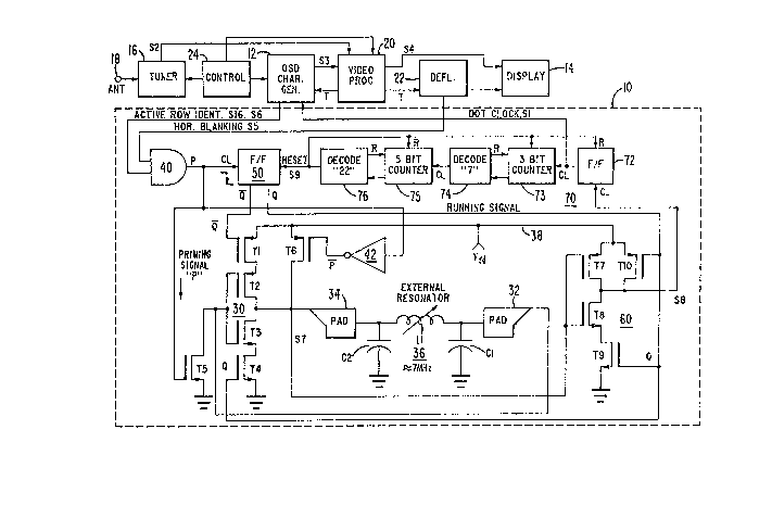
The television receiver of FIGURE 1 includes a
start-stop oscillator 10 (ou-tlined in phantom) for
supplying a character dot clock signal S1 -to an on-screen
display (OSD) character generator 12. In this application
the ON-OFF duty cycle of oscillator 10 can be expected to
vary over a wide range of values depending on the number of
lines of characters to be displayed on the receiver display
14 and so, as previously explained, there is a particular
need for the improved efficiency and low power dissipation
features of the invention. As an overview, these
advantages result, in part, because the starting or
"priming" power for the oscillator is applied only during
the horizontal blanking interval immediately preceeding a
line of character dots to be displayed and not during
blanking intervals preceeding blank character lines or
during vertical blanking. As will be explained, this
operation is facilitated by control circui-try which
provides the oscillator with three dis-tinct opera-ting
-5~ ~ RCA 82,342
modes, ON-OFF-PRIMED, and feedback is used to force the
oscillator into its OFE mode at the end of every line of
character dots regardless of whether the oscillator will be
ON or OFF during a following line. This feature
additionally prevents the possibili-ty of the oscillator
being placed concurrently in the PRIMED and ON operating
modes without the need for complicated power arbitration
logic circuitry and improves the reliabllity and
repeatibility of generation of uniform charac-ter dots in
the overall system.
The receiver includes a tuner unit 16 having an
antenna input 18 for receiving RF modulated television
signals and an output coupled to supply a baseband video
output signal S2 to a video processing unit 20 which is
also coupled to receive a character signal S3 produced by
OSD character generator 12. Video processor 20 includes
circuitry for detecting synchronizing components of video
signal S2 and generates timing signals (T) for
synchronizing character generator 12 and deflection
processor 22. Other functions provided ~y processor 20
include inserting the character signal S3 into the video
signal S2 to generate a display video signal S4 for display
14, hue and saturation control, peaking and so forth.
Control of tuner 16, video processor 20 and OSD character
generator 12 is provided by a control unit 24 which,
illustratively, may comprise a microprocessor responsive to
user inputs for generating channel selection, character
selection and various video processing control signals.
When displaying captions, OSD generator 12 receives the dot
clock signal S1 from oscillator 10 and converts the message
information provided by control unit 24 into characters in
dot matrix form for display on unit 14 (e.g., a kinescope).
Start-stop oscillator 10, embodying the
invention, includes a complementary field-effect transistor
amplifier 30 comprising transistor T2 and T3 having gate
electrodes comlected to an input terminal (PAD 32) and
drain electrodes coIlrlected ~o an output terminal ~PAD 34j.
The input and output terminals are referred to as PADs
~L~9~
-6- RCA 82,342
because in a preferred application of the invention, all
elements of oscillator 10 are constructed in an integrated
circuit except three external components comprising a
resonator 36. The term "PAD" is short for "bonding pad" to
which the external resonator 36 is connected. Resonator 36
comprises an inductor Ll connected between input and output
terminals (PADs) 32 and 34 and a pair of shunt capacitors
C1 and C2 which couple terminals 32 and 34, respecti~ely,
to ground thereby forming the "tank" circuit of a Colpits
type of oscillator. Oscillations are produced when
operating power is supplied to the source electrodes of the
amplifier transistors T2 and T3. The component values for
L1, C1 and C2 are selected such that the nominal frequency
of oscillation is about 7 MHz in this example of the
invention. Exemplary values are 26 micro-Henries for L1 and
30 pico-farads for each of C1 and C2. A higher or lower
frequency may be used for displaying more or fewer
characters per line.
Operating current for the power input terminals
of amplifier 30 (e.g., the source electrodes of T2 and T3)
is provided by complementary field-effect transistor switch
comprising transistors T1 and T4. The conduction path of
P-type switching transistor T1 is connected between a
positive supply bus 38 (to which supply voltage Vdd is
applied) and the source of P-type amplifier transistor T2.
The conduction path of N-type switching transistor T4 is
connected between the source of N-type amplifier transistor
T3 and ground. When switching transistors T1 and T4 are
both biased ON (as will be explained) operating current is
supplied to amplifier 30 (transistors T2 and T3) and
oscillations are produced. The amplifier is disabled when
transistors T1 and T4 are OFF. In this condition no
quiescent power is dissipated in amplifier 30.
A second switch comprising a pair of
complemen-tary transistors T5 and T6 is included in
oscillator 10 for supplying direct current bias to
resonator 36. The function of this bias is to condition or
"prime" the oscillator to start with a fixed predictable
-7- RCA 82,342
phase as will be explained. Also, as will be explained,
provisions are made to ensure that the priming switches T5
and T6 are never closed when the power switches T1 and T4
are closed which otherwise could disable the oscillator and
cause a substantial power drain on the Vdd supply bus 38.
Direct current bias is supplied from bus 38 to
PAD 34 by means of the conduc-tion path of P-channel field
effect transistor T6 and is withdrawn from PAD 32 to ground
by means of the conduction path of N-channel field effect
transistor T5. When both transistors are ON, the DC bias
flows from PAD 34 to PAD 32 via inductor L1 of resonator
36. For this condition, and neglecting the resistance of
inductor L1, capacitors C1 and C2 will be charged to a
steady state voltage equal to Vdd times the ON resistance
of transistor T5 divided by the sum of the ON resistances
of transistors T5 and T6. ~hen transistors T5 and T6 are
turned OFF, the DC bias current flowing -through inductor L1
will tend to continue to flow thereby discharging capacitor
C2 and charging capacitor C1. Accordingly, the first cycle
of oscillations at the amplifier output is-n-egative going
at PAD 34 and is positive-going at the amplifier input (PAD
32).
The remaining elements of start-stop oscillator
10 provide the func-tion of controlling the amplifier power
switch (Tl,T4) and the resonator bias switch (T5,T6) in a
timed relationship with generation of characters to be
displayed so as to provide three distinc-t operating modes,
namely, PRIM~D, ON and OFF. Specifically, a priming signal
P is produced by means of an AND gate 40 having inpu-ts
connected to receive a horizontal blanking signal S5
provided by deflection processing unit 22 and an active row
identification signal S6 provided by character generator
12. Signal S6 is HIGH for each horizontal line interval of
character dots and LOW o-therwise. Accordingly, as shown in
35 FIGURE 2, the output of AND gate 40 is HIGH only during the
horizontal blanking interval (tl-t2) preceeding a line of
characters to be displayed (e.g., line 1) and is LOW at all
other times. The priming signal P is applied directly to
~g~
-8- RCA 82,342
-the ga-te electrode of transistor T5 and via inverter ~2 to
the gate electrode of transistor T6. Accordingly,
transistors T5and T6 are ON during the blanking interval
(tl-t2) of line 1 thereby priming resonator 36 as
previously explained.
The ou-tput of AND gate 40 is also connected to
the clock input CL of a negative edge triggered flip-flop
50 having true (Q) and complemented (Q-bar3 outputs
connected to the ga-tes of -transistors T4 and T1,
respectively. Accordingly, at the end of the priming
interval tl-t2, flip-flop 50 is SET by the falling edge of
priming signal P thereby turning ON the power switching
transistors Tl and T4 at the time that the priming signal P
turns the biasing transistors (T5 and T6) off. Amplifier
30 is thus turned ON and the rising voltage at its input
from PAD 32 (signal S7 in FIG. 2) and the falling voltage
at its output from PAD 34 (caused by turn-off of the bias
transistor) initiates oscillations as previously explained
which are sustained throughout most of the active portion
of line 1 by amplifier 30~
Oscillations produced by amplifier 30 are
terminated just prior to the end of line 1 (t3 in FIG. 2)
by means of a feed~ack pa-th from P~D 34 to flip-flop 50.
Two reasons for this aspect of the invention are (1) to
avoid -the possibility of amplifier 30 being ON when priming
current is applied to resonator 36 which o-therwise could
cause excessive current flow and misstiming and (2) to
ensure that the oscillator au-tomatically assumes a "powered
down" condition at the end of each row of character dots.
By this latter feature, the oscillator ON time is rendered
independent of the on period of the active row
identification signal and so external ON cycle timing is
not re~uired. The feedback path which provides these
features includes a pulse shaping circui-t 60 and a ccunter
chain 70 connected in cascade between the output (34) of
amplifier 30 and the RESET input of flip-flop 50.
Pulse-shaping circuit 60 comprises P-channel
transistors T7 and T10 and N-channel transistors T8 and T9
~s~
~9- RCA 82,342
connec-ted to form a complementary field-effect transistor
N~ND gate. The gates of transistors T7 and T8 are
connected to receive the oscillator output signal S7 and
the gates of transistors T9 and T10 are connected to
receive the true (Q) ou-tput signal of flip-flop 50. As
shown in FIGURE 2 -the oscillator output signal rises to
about half the supply voltage during the priming interval
tl-t2. This "half-voltage" condition could lead to an
inde-terminate logic state in CMOS circuits because logic
threshold voltages in such circuits can vary over a
relatively wide range. This problem is avoided by shaping
circuit 60 which forces the output signal S8 to be at a
definite logic state (HIG~ in this case) whenever flip-flop
50 is RESET (i.e., during the horizontal blanking interval
as shown in FIGURE 2).
Counter 70 counts cycles of the pulse-shaped
oscillator output signal S8 to generate the dot clock
signal S1 for OSD character generator 12 and the feedback
signal S9 for resetting flip-flop 50 which stops the
os,cillator after 308 cycles have occurred. ~ounter_70,
comprises a flip-flop 72 which divides the 7 MHz shaped
amplifier output signal by two to generate the dot clock
signal Sl. The output of flip-flop 72 is divided by 7 by
means of a 3-bit counter 73 and decoder 74 and this output
is further divided by 22 to produce the reset signal S9 by
means of a 5-bi-t counter 75 and decoder 76. Flip-flop 50
is thus reset after 154 cycles of the dot clock signal Sl
have occurred in a line which corresponds to 308 cycles of
the amplifier output signal S7. The number 154 is
determined by multiplying the number of characters per line
times the number of horizontal dots per character plus
spacing (i.e., 22 x 7). For this example, it is assumed
that the characters are 5 dots wide and spaced apart by 2
dots. The f~mction provided by flip-flop 72 is to ensure
that the do-t clock signal Sl has symmetrical ON and OFF
times. To ensure a consistent s-tarting phase of signal Sl,
flip-flop 72 is reset by the output of decoder 76.
-10- RCA 82,342
Counters 73 and 75 are also reset by signal S9 to provide a
consistent starting count.