Note: Descriptions are shown in the official language in which they were submitted.
~Lf~3~
BACKGROUND OF THE INVENTION
The present invention is directed to decoder
circuits, and more particularly to a 1-of-N decoder
that places a predetermined binary level signal on one
of a multiplicity of output lines in response to a
multibit input signal.
Decoder~ of this ty]pe are commonly used to
address random access and read only memories. To
addre~s the cells in a particular row of the memory, a
word line connected to all of the cells in that row is
brought to a predetermined binary state, e.g., high.
All of the other word lines connected to the remaining
rows of cells of the memory remain in a binary low
state, so that only the information stored in the
selected row o~ cells will be sensed through bit lines
connected to the respective columns of cells. The 1-
of-N decoder serves to bring the selected word line to
the binary high state in response to an address word
from a control CP~ or the like.
In the past, standard decoder circuits have
generally fallen into one of two categories. One
category of decoders is comprised of only bipolar
transistors using emitter coupled logic. The other
category of decoders employs field e~fect transistors.
Decoders in this latter category can be comprised
entirely of field e~fect transistors, e.g., CMOS
circuit arrangements, or a combination of bipolar NPN
transistors with both N- and P-channel MOS transistors,
i.e., BICMOS circuits.
Each of the two categories of decoder
circuits has its attendant advantages and limitations.
For example, the decoders which use MOS devices have
essentially no static power dissipation, since current
is drawn only when switching from one state to another.
In contrast, the ECL decoder draws a much more
73~j
significant current ~ven while it is in an idle state.
However, decoders which use BICMOS technology
are more expensive to manufacture because they require
more masking steps to provide each o~ the bipolar NPN
transistors, PMOS and NMOS field effect transistors
during the fabrication of the integrated circuit. In
addition, they must be fed wit:h standard CMOS voltage
levels, which are higher than those needed in the
strictly bipolar approach.
Another advantage which the ECL decoder
attains over the known FET-based circuits pertains to
the output signal reference levels. In the bipolar ECL
approach, the binary level signals on the output lines
are referenced only to a single power source voltage.
For example, a logic high signal might be at or quite
near the higher power source voltage, and logic 13w
might be a predetermined voltage below the high level.
In contrast, the logic signals ~hat are produced with
the MOS decoder circuits are a function of both the
high and low power supply levels. In other words, the
logic high signal *ollows the higher power source
voltage Se.g., Vcc) and the logic low follows the
ground reference voltage. A problem associated with
this latter arrangement is that transient signals~
i.e., logic swings, are dependent upon power supply
noi~e and voltage variations.
BRIEF STATEMENT OF THE INVENTION
Accordingly, it is an object of the present
invention to provide a novel decoder that incorporates
the advantageous features of both bipolar and BICMOS
decoding circuits without their individual attendant
limitations notad above. In accordance with the
present invention, this objective is achieved throu~h
the use of BIPMOS technology which includes both
bipolar NPN and P-channel MOS transistors. Since this
~.2~5735
62957-250
technology does not include N-channel transistors, fewer masking
steps are required to produce the clrcuit, thereby resulting in a
lower ~ost. However, the circuit retains almost all of the power
saving advantages of conventional BICMOS decoders. In accordance
with a further feature of the invention, transient signals are
re~erenced to one power supply voltage only, to thereby make the
logic swing and performance characteristics of the decoder
independent of power supply voltage variations. Therefore lt
becomes possible to use PMOS transLstor~ that have smaller voltage
requirements than conventional CMOS circuits. In the arranyement
of the present invention, the PMOS transistors are used to control
the operation of the bipolar transistors. Accordingly it is only
necessary to operate the PMOS transistors with relatively small
drain voltage variations, since the bipolar transistors are
sensitive to such small variations.
In accordance with the invention there is provided l-o~-
N2 decoder having N2 output lines each of which carries a binary
logic signal with a value that is referenced to only a single
power source voltage, comprising,
a pair of 1-of-N predecoders each having N control lines
and being responsive to an input signal to produca a signal at one
binary voltage level on one of said control lines and a aignal at
a complementary binary level on the other N - 1 control lines;
N2 p-channel MOS transistors each having a drain-source
current path connected between said power source voltage and a
current sink commonly connected to all of said MOS transistors
through respective loads;
".~
~2~357~35
62957 250
N2 bipolar NPN transistors each having a collector connected
to said power source voltage and an emitter connected to a current
sink common to all of said bipolar transistors, the collector-
emitter paths of said bipolar transistors being respectively
connected to said N2 output lines, each of said bipolar
transistors having a base that is connected to the drain-source
current path of a respective one of said MOS transistors; and
logic selection means connected to the yates of sald MOS
transistors and responsive to the binary signals on the control
lines of said predecoders to cause one of said MOS transistors to
conduct current along lts drain-source current path and thereby
actuate the bipolar transistor connected to said one MOS
transistor so that said bipolar transistor conducts current and
produces on the associated output line a binary signal having a
predetermined voltage relative to said power source voltage.
In accordance with the invention there is also provided
a l-of-N2 BIPMOS decoder circuit comprising:
a predecoding circuit which receives an input signal and
produces a logic output signal designating one of N possible
output conditions indicated by said input signal;
N decoding gates respectively producing said N output
conditions, each of said decoding gates includlng:
at,least one p-channel MOS transistor having a gate electrode
for receiving a binary logic signal resulting from the logic
outpu-t signal of said predecoding circuit,
a bipolar output transistor having a base electrode connected
to a drain of said MOS transistor ~uch that said bipolar output
., , 3a
~ .
~ ~5,t7~35
62g57 250
transistor is rendered selectively conductive in response to the
state of the binary logic signal at the gate electrode of said MOS
transistor,
an output terminal connected to one of the colleckor and
emitter of said bipolar translstor, and
a current sink connected in common to the drain of the MOS
transistor in each of said N gates.
In accordance with the present invention there is also
provided a decoder circuit comprising:
a first plurallty of predeaoding means;
a second plurality of MOS logic gates, each fabricated using
a single MOS process and comprising at least a flrst plurality of
MOS transistors, raceiving a first plurality of signals one from
each said predecoding means, each sald gate being connected to a
first current sink, only one of said gates drawlng a conductlon-
level current at any given time; and
a second plurality of bipolar transistor drives, each
receiving a signal from a different one of said gates and driving
a separate output line in dependence thereon, each said translstor
being connected to a second current sink, only one of said
transistors drawing an appreciable current at any given time.
Further features and advantages of the present invention
are explained in detail hereinafter with reference to preferred
emhodiments illustrated in ~he accompanying drawings.
BRIEF DESCRIPTION OF THE DRAWINGS
Figure 1 is a block diagram of an exemplary circuit in
which the decoder of the present invention can be utilized;
3b
735
62957-250
Figure 2 is a schematlc diagram of a prior art bipolar
decoder circuit;
Figure 3 is a schematic diagram o~ one embodiment of a
decoder which incorporates the present invention;
Figure 4 is a schematic ~diayram of a second embodiment
of a decoder gate according to the present invention;
3c
573S
Figure 5 is a schematic diagram of a
variation of the embodiment shown in Figure 4: and
Fiyures 6A-6D are schematic circuit diagrams
of other variations o~ the second embodiment o~ the
invention.
DESCRIPTION OF THE ILLUSTRATED EMBODIMENTS
As briefly described above, 1-o~-N decoders
are commo~ly employefl as memory control circuits. An
application of such a decoder is illustrated in Figure
1. In this example, the memory circuit 10 to be
controlled is an ~ x M memory having N word lines 12
and M bits of information per word. For example, the
number o~ word lines, N, might be 256 and the nun~er of
bits per word, M, might be 32, to provide an 8X memory.
This memory can be either a read/write random access
memory (RAM) or a read only memory (ROM).
In operation, all of the word lines 12 are
held at a preselected binary state, eOg., logic low, by
a l-of-256 decoder 14. When lt is desired to read a
particular 32-bit word of in~ormation, the address o~
that word is indicated by an 8-bit address signal
applied to the dacoder. The address signal causes the
decoder to bring the ~ignal on a selacted word line to
a logic high level while maintaining all of the other
word lines at the logic low level. When the selected
word line is brought to the logic high level, it
becomes possible to sense the value of each of the 32
bits in the word associated with that word line by
means of bit lines 16 in the memory.
In the following description of pre~erred
e~bodim~nts of the present invention, reference is made
to the use o~ the invention in a memory rontrol
environment of the type depicted in Figure 1. Such
reference i9; made for the purpose of facilitating an
understanding o~ the inventive concepts and their
;73~ii
applications. However, it will be appreciated by those
having familiarity with the applicable art that l-of-N
decoder cixcuits can be used in other applioations, and
the illustrative reference to memory circuit control is
not intended in any way to be a limitation on the
invention or its applications.
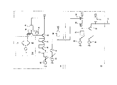
Referring now to Fic~re 2, a prior art
bipolar decoder circuit using emitter coupled logic is
illustrated. In operation, an 8-bit address signal
from a CPU or the like is divided into two 4-bit
signals, each of which is fed to a 1-of-16 predecoder
18. In response to the applied input signals, each
predecoder 18 causes one of its 16 output lines to go
to a logic low level, while maintaining the other 15
output lines at a logic high level. One output line
from each of the two 1-of-16 predecoders is fed to a
gate 20, only one of which is shown in Figure 2. In
practice 256 (i.e., 16 x 16) gates are employed, with
each having a different combination of inputs from the
two respective predecoders 18.
In ea~h gate 20, the pair of input lines ~rom
the 1-of-16 predecoders are respectively connected to
the bases of two NPN transistors 22 and 24 connected in
parallel to form a NOR gate. The collectors of these
2~ two transistors are connected to a positive power
supply voltage Vcc by means of a pull-up resistor 25,
and the emitters of these two transistors are connected
to a current sink 26, e.g., a ground reference
potential~ Another NPN transistor 28 is connected to
the transistors 22 and 24 by means of a common emitter
configuration to foxm a difference amplifier.
suitable reference voltage is applied to the base of
the transistor 28. This voltage reference might be at
a~out the midpoint of the logic high and logic low
voltage levels produced on the output lines of the 1-
of-16 decoders 1~. In operation, the l-of-16
735
predecoders normally hold the bases of the transistors
22 and 24 at a logic high level, so *hat thesP
transistors are conductive. In this case, a current Is
is conducted through these transistors. When both of
S the input lines to the gate 20 are brought low by the
predecoders, the transistor 28 becomes conductive to
carry the current Is~
The collectors of the transistors 22 and 24
are also connected to the bas;e of an emitter follower
transistor 30. The collector of this transistor is
connected to the positive power supply voltage Vcc and
its emitter is connected to a current sink 32 by means
of a pull-down resistor 34. The current sink 32 is
connected in common with a corresponding emitter
follower transistor in each of the other 255 yates in a
similar manner by means of respective pull-down
resistors. The junction between the emitter of the
transistor 30 and the pull-down resistor 34 is
connected to an associated word line of the memory
unit.
In operation, when either of the transistors
22 or 24 is conductive, it causes the current Is to be
conducted through its collector and the pull-down
resistor 25, thereby holding the base of the transistor
30 at a low voltage level. Consequently, this
transistor is maintained in a non-conductive state, and
the associated word line is at a logic low level. Upon
coincidence of a low signal at each of the two input
lines from the predecoders, the resistor 25 supplies
current to the base of the transistor 30 to render it
conductive. This causes the signal on the associated
word line to go high. At this time, the current Is is
steered through the transistor 28.
It will be appreciated that the total current
reguired by a 1-of-256 decoder of the type represented
in Figure 2 is equal to 256 Is + Id since each of the
~.2~7~
gates draws a current Is regardless of its state of
actuation, and the selected gate also draws a current
Id through its pull-down resistor 34. These
substantial power requirement~; impose a serious
limitation on the speed of the decoder. More
particularly, if the number o~ gates is increased to
accommodate a greater number of word lines, the time
required to access each word alddress increases i~ a
constant power is supplied. ]n order to decrease
access time it becomes necessary to increase the power
that is available to the decocler.
In accordance with the present invention, the
power reguirements of a l-of-N type decoder can be
significantly reduced by utilizing a combination of
bipolar and P-channel MOS devices. One example of a
decoder circuit which achieves this objective is
illustrated in Figure 3. Because of its reduced power
requirements, an increase in the number o~` word lines
will have a minimal impact on the operating speed o~
the decoder.
Referring to Figure 3, 4 bits of the address
signal are respectively applied to 4 input buffers 36
in a l-of-16 predecoder 35. Only one of these buffers
is shown in the figure. The input bu~fer essentially
comprises a common emitter difference circuit in which
the base of one transistor receives a bit of the input
signal and the base of the other transistor is
connected to a suitable reference ~oltage. The
~ollector of one o~ these two transistors is connected
to an emitter of a multiple emitter transistor 38. The
other emitters of this transistor are connected to
similar buffer circuits in a known manner to form a
logic selection circuit corresponding to the address o~
one o~ 16 possible output lines. The base of the
multiple emitter tran~istor 3~ is connected to the
positive power supply voltage Vcc by means o* a first
57~
resistor 40, and also connected to its collector by
means of a second resistor 42. In turn, the collector
is connected to the base of a first transistor in a
series of emitter follower and level shiPting
transistors 44, 46 and 48. The emitter of this last
transistor is connected to a current ~ink 50 by way o~
a pull-down resistor 52 and also to the base of a
switching transistor 54. The emitter of the switching
transistor 54 is connected to a second current sink 56,
a~d its collector is connected to the positive power
supply voltage Vcc through a pull-up resistor 58. The
collector is also connected to an output line which
comprises one of the 16 output lines o~ the predecoder.
Each predecoder comprises 16 circuits of the
type depicted in Figure 3. However, the currenk
sources 50 and 56 are connected in common to each of
the resistors and transistors corresponding to the
pull-down resistor 52 and output transistor 54,
respectively, of the 16 circuits.
In operation, any 4-bit input signal will
correspond to the logical arrangement of the input
buffers and multi-emitter transistor 38 of one of the
16 salection circuits, causing its multi-emitter
transistor to turn off. When this occurs, the level
shifting transistor 44 and the diode~connected
transistors, 46, 48 are each rendered conductive to
pre~ent a relatively positive voltage at the emitter of
the ~inal transistor 48. The current sink 50 will
therefore conduct current for the selected one, and
only the selected one, of the 16 possible paths. This
current will render the switching transistor 54
conductive to bring the output line associated with
this transistor to a logic low level. Preferably, the
value o~ the pull-up resistor 58 is chosen so that the
voltage drop that is achieved across this resistor is
125~5 ~35
less than the level shift produced by the transistors
44-48. With this arrangement, saturation of the
switching transistor 54 is avoided, to achieve faster
response times.
In an associated gate 59, a pair of input
lines from two l-of-16 predecoders 35 are respectively
applied to the gate electrodes of a pair o~ P-channel
MOS transistors 60 and 62 hav:ing their drain-source
current paths connected in series between the positive
power supply voltage Vcc and the base of a bipolar NPN
switching transistor 64. The P-channel transistors 60
and 62 are also connected, by means of a pull-down
resistor 65, to a current sink 66 that is common to all
of the 256 gates. The emitter of the switching
transistor 64 is connected to a second current sink 68
that is likewise common to all of the gates. The
collector of the switching transistor is connected to
an output word line 12 and to the positive power supply
voltage by means of a pull-up resistor 69.
In operation, the switching transistor 64 of
one of the gates 59 is selected by the coincidence of a
negative voltage at the gate electrode of each of its
two associated P-channel transistors 60 and 62. When
the switching transistor 64 is actuated, it-pulls the
associated word line low. Almost all of the common
current ~or the decoder is fed inko the selected word
line because the base voltage of the switching
transistor 64 is more positive than that of the other
transistors which share the same emitter current sink
68. For example, at room tempexature, a 204 mv
di*ference between the most positive base and the other
bases will cause 90~ of the common current of the
current sink 68 to flow through the selected switching
transistor 64, leaving the other 10% to be shared by
the 255 unselected gates. Since most of the power
flows through the selected gate, the power dissipation
--10--
of thQ circuit is constant and no large transients
occur during switching.
Furthermore, the output signals of the
decoder, i.e., the logic high and low levels, are
referenced only to the Vcc power supply. Thus, logic
swings are substantially independent of power supply
noise andrvoltage variations.
In the circuit illustrated in Figure 3, the
logical "AND" function for detecting the coincidence o~
two low level input signals is per~ormed by the series
connected P-channel transistors 60 and 62. In some
cases, it may be preferable to have this logical
function accomplished using bipolar logic. Such an
arrangement is illustrated in a second embodiment of
the invention shown in Figure 4. In this embodiment,
each of the l-of-16 predecoders 35 can have the same
structure as those shown in Figure 3. However, the
switching transistor 54 and second current sink 56 can
be eliminated so that the emitter of the level shifting
transistor 48 is directly connected to the output line
of the predecoder to provide a logic high selection
signal.
In the gate circuit shown in Figuxe 4, a
single current through a sink 70 is steered into 1 of
256 possible paths through two tiers of current
switches. The first tier is formed by bipolar NPN
transistors 72-73 each having its base connected to a
separate output line of one of the 1-o~-16 predecoders
35. Since only one of these transistors will be
activated by the selected high output signal from the
predecoder, it will st~er the current to one of 16
second tiers. Each of these second tiers comprises 16
bipolar transistors whose bases are respectively
connected to the 16 output lines o~ the second
predecoder. The collector of each of these second tier
transistors is connected to a separate word line by
r5 7 3 ~i
means of a circuit such as that shown in Figure 4.
When the first tier transistor 72 and the second tier
tran~istor 74 associated with a particular word line
are both actuated, they develop a voltage across a
pull-up resistor 76 to render conductive a P-channel
MOS transistor 78 ~which corr~esponds to one of the MOS
transistors 60 and 62 of the first embodiment). The
value o~ the resistor 76 is preferably chos n so that
the second tier transistor 74 does not saturate when it
is actuated. In response to the conduction o~ the PMOS
transistor 78, a bipolar NPN transistor 80 is actuated
in the same manner as the switching transistor 64 o~
the first embodiment.
The preceding embodiments of the invention
have ~een illustrated for the case in which the
selected word line is pulled to a logic low level to
access the information in the memory. However, the
invention is equally applicable to situations in which
the word lines are normally held in a low state and the
selected line is pulled to a logic high level. One
example of a circuit for operating ir. this mode is
illustrated in Figure 5. All of the components of the
decoder are essentially the same as in the embodiment
- of Figure 4, except for the connections of the
switching transistor 80. In this regard, the collector
of the transistor is directly connected to the positive
power supply voltage Vcc, and its emitter is connected
to the output word line 12 to provide an emitter
follower arrangement. The emitter is also connected to
the common current sink 81 by means of a pull-down
resistor 82.
Si~ilar to the considerations for tAe
transistors 54 and 74 in the predecoder circuits of
Figures 3 and 4, respectively, performance of the
decoder is improved by limiting the current flowing
through its output transistor (64 or 80) to prevent
saturation. This current limiting can be done through
appropriate selection of the pull-up or pull-down
resistor connected to the collector or emitter,
respectively, of this transistor. Alternatively,
saturation can be prevented by suitable clampinq and
feedback techniques. Examples of these techniques are
illustrated in Figures 6A-6D.
It will be appreciated by those of ordinary
skill in the art that the present invention can be
embodied in other specific forms without departing from
the spirit or essential characteristics thereof. The
presently disclosed embodiments are therefore
considered in all respects to be illustrative and not
restrictive. The scope of the invention is indicated
by the appended claims rather than the foregoing
description, and all changes that come within the
meaning and range of equivalents thereof are intended
to be embraced therein.