Note: Descriptions are shown in the official language in which they were submitted.
~L.h.,~ ~; 7,. i 7
- I - RCA 84,0"?
FET TUNER
Related Applications
Canadian application serial number 552851-8 entitled "Wide
Range Oscillator" and Canadian application serial number 552852-
6 entitled "Dual Gate Tunable Oscillator" concurrently filed in the
name of the same inventor are related applications.
Field of the nventlon
The present invention is in the field of tuning systems.
Background of the Invention
Tuning systems for radio and television receivers typically include
a tunable RF stage for selecting the RF signal corresponding to a
desired station or channel from a plurality of received RF signals,
a tunable local oscillator for generating a local oscillator signal
having a frequency corresponding to the desired station or
channel and a mixer for heterodyning the selected RF signal with
the local oscillator signal to produce an IF signal corresponding to
the RF signal. Typically, both the RF stage and local oscillator
include respective varactor diodes which are responsive to a
tuning voltage.
In many applications, the RF stage and local oscilla~or should
be capable of being tuned over a relatively wide tuning range in
substantial tracking relationship to ensure mixing of the
appropriate RF signal and local oscillator signal for each channel
with each other throughout the tuning range.
;. ,.i
:
-2- ~ 757 RCA 84,092
Summary of the Invention
Ic is herein recognized that when the RF stage
and the local oscillator both include field effect
transistors arranged in the same amplifier configuration
and coupled to tuned circuits of substantially the same
configuration, the tracking characteristics of the tuner
are
improved.
Brief Descrip-tion of the Drawin~
FIGURE 1 is a schematic diagram showing a tuner
of a television receiver embodying the present invention;
E'IGURE la is a schematic diagram of an equivalent
circuit useful in understanding an aspect of the local
oscillator shown in FIGURE l;
FIGURE lb is a schematic diagram of a
modification to the local oscillator shown in FIGURE l;
FIGURE lc is a schematic diagram of an equivalent,
circuit useful in understanding the modification shown in
FIGURE lb; and
FIGURE 2 is a schematic diagram showing in detail
the RF stage of the tuner shown in block form in FIGURE 1.
In the FIGURES, various exemplary element values
are identified in parenthesis. Unless otherwise indicated,
resistance values are in ohms, the capacitance values are
in picofarads and the inductance values are in nanohenries.
Further with regard to the exemplary values, K represents
1000, M represents 1,000,000 and ~ ~micro) represents
O.000001.
Description of the Preferred Embodiment
FIGURE 1 shows the VHF section of a tuner of a
television receiver for tuning VHF broadcast and VHF cable
channels. RF signals provided by a source (not shown) such
as an antenna or cable distribution network are coupled via
an RF input 1 to a tunable RF stage 3. RF stage 3 selests
the RF signal corresponding to a desired channel in
ii7~
-3- RCA 8~,092
response to the magnitude of a tuning voltage (TV). The
selected RF signal is coupled to a mixer 5 where it is
heterodyned with a local oscillator signal generated by a
local oscillator 7 having its fre~uency of oscillation
controlled in response -to the magnitude of the tuning
voltage to produce an IF signa:L corresponding to the
selected RF signal.
A tuning control unit 9 generates the tuning
control voltage. Tuning control unit 9 also generates
bandswitching voltages (BSl and BS2) for selecting
inductors to be included in fre~uency selective tuned
circuits of RF stage 3 and local oscillator 7 in accordance
with the tuning band of the desired channel. By way of
example, tuning control unit 9 may include a phase~locked
loop (PLI,) type of frequency synthesizer for converting
binary coded represen-tations of the channel number of the
desired channel to a tuning voltage of -the appropriate
magnitude and a logic network for generatin~ the
appropriate bandswitching voltage in response to the binary
2Q coded representations of the ch2~nel ~um~er.-
Bandswitching voltages BSl and BS2 can haveeithex a low level, e.g., -12 volts, or a high level, e.g.,
+12 volts. The tuning bands and the respective levels of
bandswitching voltages BSl and BS2 are indicated in the
following table.
CHANNEL RF FREQUENCY LO FREQUENCY
B BS2 NOS. RANGE (MHz~ RANGE (MHz)
LOW LOW 2 thru 6 55-88 101-129
HIGH LOW A-5 thru 13 91 216 137-257
HIGH HIGH J thru W+28 217-468 263-509
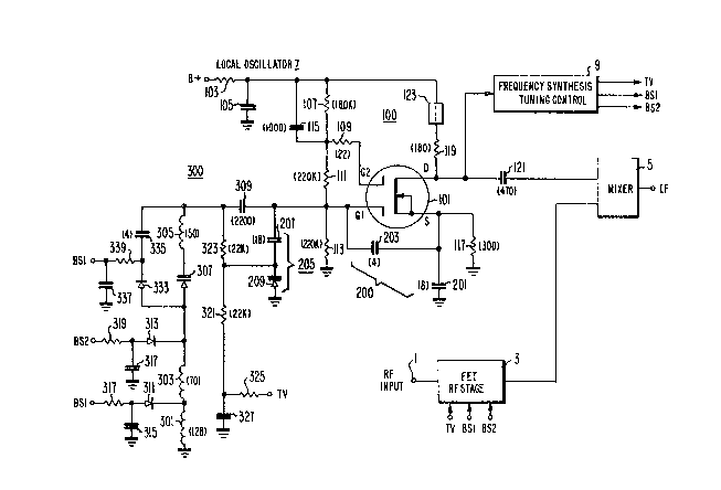
Local oscillator 7 comprises an amplifier 100
including a dual ga-te N channel metal oxide semiconductor
(MOS) field effect transistor (FET~ 101 having a first gate
electrode (Gl), a second gate electrode (G2), an N-type
conduction channel connected at one end to a source
electrode ~S) and at the other end to a drain electrode
(D). The voltages at the gate electrodes dcterminc thc
degree of conduction of the conduction channel. A source
of positive supply vol-tage (B+), e.g., +12 volts, is
~ 7~ RCA ~,092
provided by tuner control unit 9 when a VHF channel is
selected. The positive supply voltage is ~iltered by a
lowpass filter including a resistor 103 and a capacitor
105. The power supply return path is connected -to signal
ground. A vol-tage divider network including resistors 107,
109, 111 and 113 connected to the ga-te electrodes biases
FET 101 to operate as linear amplifier. Resistor 109
serves to inhibit unwanted parasitic oscillations of FET
101 .
In local oscillator 7, amp].ifier 100 is
configured as a cascode amplifier by utilizing the firs-t
gate electrode (Gl) of FET 101 as the inpu-t, effectively
connecting the second gate electrode (G2) to sigrlal ground
through a bypass capacitor 115 (no-ting that resistor 109
has a very small value), coupling the source electrode (S)
to signal ground through a resistor 117, and utilizing the
drain electrode (D) as the output of the amplifier. The
drain electrode (D) is coupled to the B+ power supply
conductor through a load resistor 119 and to mixer 5
through a large valued DC blocking capacitor 121. A
ferrite bead 123 is provided on the conductor between load
resistor 119 and the B~ conductor as an inductive AC
blocking filter element. The configuration of FET 101 may
be thought of as a cascode amplifier because the first gate
electrode (G1), the source electrode (S) and the lower end
of the conduction channel are configured as a common source
amplifier and the upper end of the conduction channel, the
second gate electrode (G2) and the drain electrode (D) are
configured as a common gate amplifier.
A circuit 200 for conditioning amplifier 100 to
oscillate is coupled between the first gate electrode (G1)
and the source electrode (S). A series tuned circuit 300
responsive to the tuning voltage (TV) for determining the
particular frequency of oscillation is coupled between the
first gate electrode (G1) and signal ground.
Oscillator 7 is conditioned to oscillate in the
following manner. In general, an amplifier will oscilla-te
if two condi.tions are met: (1) there is zero phase shift
around a loop including a path from the input to the output
~ ~Za3~; 7 ~7
- 5 - RCA 84.09
of the amplifier and a path from the output to the input; and (2)
the gain around the loop is greater than unity. In the case of
oscillator 7~ the portion of FET amplifier 100 including the first
gate electrode (Gl), the source electrode (S) and the lower end of
the conduction channel is conditioned to oscillate. While this
portion is a common source amplifier, with regard to the cascode
amplifier configuration of FET 101, it is a common drain or source
follower amplifier, with an input at the first ga~e electrode (Gl)
and the output at the source electrode (S), with regard to the
oscillation configuration. Oscillation conditioning network 200,
connected between the output of the common drain amplifier
configuration at the source electrode (S) and the input at the first
gate electrode (Gl), includes a capacitor 201 connected in shunt
with resistor 117 between the source electrode (S) and signal
ground and a capacitor 2()3 connected between the source
electrode (S) and the first gate electrode (Gl). As will be
appreciated, this configuration is of the Colpitts ~ype.
With respect to the phase shift requirement for
oscillation, there is subs~antially no phase shift between the input
(Gl) and the output (S) and there is a phase lag contributed by
capacitor 201 and a compensa~ing phase lead contributed by
capacitor 203 between the output (S) and the input ((:;1). With
respect to the gain requirement for oscillatioll, there is a voltage
gain of slightly less than one due to source ~ollower operation
between the input (Gl) and the output (S) but a voltage increase
("step-up") due to capacitors 201 and 203 between the output (S)
and the input (Gl). As a result, the conditions for oscillation are
met and the source follower configuration will oscillate at the
frequency determined by tuned circuit 300. The current through
the resistor 117 connected to the source electrode (S) and through
the conduction channel varies with the oscillation and the voltage
across load resistor 11 9 connected to the drain electrode (D)
varies accordingly.
" ..,
-6- ~2~r57~7 RC~ 84,092
The cascode amplifier configuration of EET 101 is
advantageous in several respec-ts. The common gate
amplifier portion provided by bypassing the second gate
electrode (G2) to signal ground substantially isolates the
oscillatory por-tion from mixer 5 while addi-tionally
enabling mixer 5 to be driven at appropriate sigrlal and
impedance levels without -the need for a separate buf~er
amplifier device. Due to the common gate amplifier
portion, a virtual ground is e:Efectively presented to the
output of the common source amplifier portion so that
impedance variations exhibited by the mixer, due, e.g., to
amplitude variations in the RF signal coupled to it from RF
stage 3, do not substantially effec-t either the frequency
of oscillation or the conditions for establishing
oscillation. Moreover, because of the isolation, the drive
requirements of mixer 5 do not have to be compromised to
satisfy the conditions necessary for oscillation.
Another advantageous feature of FET local
oscillator 7 is realized when it is employed with an FET RF- 20 stage. Many tuners llsed in television r~siver~--em~lGy
dual gate FET RF stages because they produce relatively low
distortion and have relatively high impedances compared
with bipolar transistor RF stages. In addition, the second
gate electrode provides a convenient means for applying an
automatic gain control (AGC~ voltage. A dual gate FET RF
stage suitable for use as RF stage 3 is shown in FIGURE 2
and will be explained in detail below. Briefly, the RF
stage shown in FIGURE 2 includes an amplifier 400 including
a dual gate N MOS FET 401 configured, like FET 101 of local
oscilla-tor 7, as a cascode amplifier with the input at the
first gate electrode (Gl), the second gate electrode G2
effectively connected to signal ground through a bypass
capacitor, the source electrode (S) coupled through a
resistor to signal ground, and the output derived a-t the
drain electrode (D). RF input 1 is coupled to the input
(Gl) of FET amplifier 400 through a series tuned circuit
500 responsive to the -tuning voltage (TV). The output of
FET amplifier 400 is coupled through a doubly tuned filter
i'7~7
- 7 - RCA 84,09
600, comprising two inductively coupled series-tuned circuits 601
and 603 each responsive to the tuning voltage (TV), to another
dual gate FET amplifier 700 also configured in cascode
configuration. The output of dual gate FET amplifier 700 is
coupled to mixer 5. Since RF stage 3 and local oscillator 7 have
amplifiers of the same device type and configuration and have
similar tuning configurations, it has been found that the ability to
track one another in frequency in response to the tuning voltage
is improved compared with a conventional arrangement in which
the RF amplifier is of the dual gate FET type and the local
oscillator is of the bipolar type.
Returning now to FIGUR~ 1, tuned circuit 300 will be
described in detail. As earlier noted, tuned CiTCUit 300 is a series-
tuned circuit. Tuned circuit 300 includes indllctors 301, 303 and
305, a varactor diode 307 connected in series with a DC blocking
capacitor 309 between the input (Gl) of amplifier 100 and signal
ground. Inductor 5 is coupled in series between varactor diode
307 and the input (Gl) of amplifier 100. This has been found to be
a beneficial configuration since the inductor 305 tends to isolate
varactor 305 from stray capacitances exhibited at the input of
amplifier 100. Bandswitching diodes 313 and 311 and associated
bypass capacitors 315 and 317, respectively, selectively bypass
the circuit point intermediate inductors 301 and 303 and the
circuit point intermediate inductor 303 and varactor diode 307,
respectively, to signal ground in accordance with the levels of
bandswitching voltages BSI and BS2. Bandswitching voltages BSI
and BS2 are coupled to bandswitching diodes 313 and 315
through respective high valued isolation resistors 318 and 319,
respectively. The tuning voltage ~TV) is filtered by a lowpass
filter including a resistor 325 and a capacitor 327 and coupled to
the cathode of varactor diode 307 through isolation resistors 321
and 323 and inductor 305.
An oscillation range extending circuit 205 associated with
oscillation conditioning network 200 includes a capacitor 207 and
a varactor diode 209 directly
"
~.
i 7
-3- RCA 8~,092
connected in series be-tween the inpu-t (Gl) of amplifier lO0
and signal ground without any intervening elements that
would present significant impedance in the frequency range
of interest. Capacitor 207 has a capacitance value
selected so that it appreciably effec-ts the combined
capacitance of capacitor 207 and varactor diode 209. In
practice, the specific value of capacitor 207 can be
selected to control the range extension and the tracking of
local oscillator 7 wi-th RF stage 3. The tuning voltage
(TV) is coupled to the cathode of varactor diode 331
through isolation resistor 321. Varactor diodes 307 and
209 are poled with respect to the tuning voltage so that
the capacitances they exhibit change in the same sense in
response to changes in the magnitude of the tuning voltage.
Range-e~tending circuit 205 extends -the oscillation range
of oscillator 7 in the following manner.
The equivalent circuit exhibited by amplifier 100
a-t its input (Gl) in the range of oscillation is shown in
FIGURE la and includes an e~uivalent capacitance element
-- - 20 (Ceq) and a negative resistance element (-~.eq~-connected in
series between the first gate electrode (G13 and signal
ground. The negative resistance element (~Req) is related
to the gain exhibited by the oscillation portion of
amplifier 100. The equivalent circuit exhibited by -the
25 series-tuned circuit 300 including inductors 301, 303 and
305, varactor diode 307 and DC blocking capacitor 309 at
the input (Gl) of amplifier 100 includes a variable
capacitance element (CT), a resistance element (RT) and an
inductance element (LT) connected in series between the
first gate electrode (Gl) and signal ground. Since DC
blocking capacitor 309 has negligible impedance in the
frequency range of interest, the variable capacitance
element (CT) essentially exhibits the capacitance of
varactor diode 307. The resistance RT corresponds to the
loss associated with the tuned circuit, which is primarily
associated with varactor diode 307. To sustain oscillation
throughout the range of interest (101-509 MHz), the
magnitude (Reg) of the negative resistance element (~Req)
- 9 - RCA 84,09
associated with amplifier 100 must be greater than the magnitucle
of the resistance element (RT) associated with tuned circuit 300.
The particular frequency of oscillation is inversely related to the
square root of LTC, where C is the combined capacitance of CT ancl
Ceq. The combined capacitance of CT and Ceq is given by
CTCeq/CT+Ceq. For a wide tuning range, Ceq should be as large as
possible with respect to the largest value of CT (corresponding tO
the lowest frequency of oscillation) so that C can undergo
substantially the full range of change of varactor diode 307 (CT).
Adding a fixed capacitor in shunt with the input of
amplifier 100 between the first gate electrode (Gl) and signal
ground increases the value of Ceq and therefore tends to extend
the tuning range at low frequencies. However, the addition of a
fixed shunt capacitor decreases R and therefore tends to prevent
oscillation, especially at high frequencies. Range extension circuit
205 connected in shunt with the input (Gl) of amplifier 100
provides a variable capacitance which increases as the tuning
voltage (frequency) decreases and which decreases as the tuning
voltage (frequency) increases. As a result, Ceq is the largest when
CT is the largest (i.e., at low frequencies) but a value Req
sufficiently large to sustain oscillations is still provided at high
fre~quencies .
The direct connection of range extending circuit 205
between the input (Gl) of amplifier 100 and signal ground, rather
than through an element having significant impedance in the
frequency range of interest, ensures that it will have an
appreciable effect on the input capacitance (Ceq) of amplifier 100.
With regard to range extension network 205, it is
noted that while a dual gate FET has the advantages described
above, its gain (and therefore Req) is lower than that of a bipolar
transistor configured in comparable fashion as a common collector
Colpitts type oscillator with its base electrode coupled to a tuned
circuit, i~s emitter electrode coupled to signal ground through an
impedance and
,:, '.1~
- l o ~ 5~ RC~ 8~,092
its collector electrode serving as the output electrode.
I'herefore, while range extension circuit 205 may be
utilized to extend the t-uning range of a Colpitts type
bipolar transistor oscillator, its advantages are even more
significant when employed with an FET oscillator as shown
in FIGURE 1.
It is known to employ a parallel tuned circuit in
place of a series tuned circuit as is shown in simplified
form (without biasing elements) in FIGURE lb. However, it
was found that when a parallel tuned circuit was utilized
in place of series tuned circuit 300 it was more difficult
to obtain the wide -tuning range required, even when a range
extending circuit was utilized as is shown in FIGURE lb.
This can be explained as follows with respect to the
equivalent circuit shown in Figure lc. In FIGURES lb and
lc, elements corresponding to the same elements in FIGURES
1 and la, respectively, are identified by the same
reference designa-tions. The primed ('~ designations
correspond to the modification of replacing the series
tuned circuit with a parallel tuned circuit. --
With respect to FIGURE lc, the frequency ofoscillation is inversely related to the square root of
LTC', where C' is the combined capacitance of C'T and Ceq.
In this case, the combined capacitance C' is given by C'T +
Ceq. For a wide tuning range Ceq should be small with
respect to the lowest value of C'T ~corresponding to the
highest frequency of oscillation) so that C' can undergo
substantially the full range of change of C'T The value
of Ceq can be lowered by connecting a low valued capacitor
in series between the parallel tuned circuit and the input
of the amplifier. However, the effective loss of the
parallel tuned circuit increases as the square of the ratio
CT/Ceq and therefore a-t the high values of CT
(corresponding to the low frequency end of -the tuning
range), the loss of the parallel tuned circuit may overcome
the gain (related to ~Req) required for oscillation.
The addition of a varactor diode connected in
series between the parallel tuned circuit and the input of
~ 757 RCA 84,092
the amplifier and poled so -that i-ts capacitance varies in
the same sense as the ~aractor diode of the tuned circuit
as shown in EIGURE lb tends to extend the tuning range by
providing compromise between a relatively low value of Ceg
at high frequencies and a relatively low effective loss at
low frequencies. ~owever, it was found that since the loss
of the parallel tuned circuit varies with the square of the
ratio CT/Ceq at -the lower frequency end of the required
tuning range, oscillation was not always reliable when an
FET was utilized rather than a higher gain (higher Req)
bipolar transistor. According:Ly, the series tuned
configuration shown in Figure L is preferred for use ~li-th a
FET.
As earlier noted, tuning control uni-t 9 may
comprise a phase locked loop. The reliable oscillation of
oscillator 7 at low frequencies is particularly important
when a phase locked loop type of tuning control system is
employed. Phase locked loop tuning control systems usually
employ a frequency divider known as a "prescaler" for
dividing the very high frequency of the local oscillator
signal before it is further divided by a programmable
frequency divider according to the channel number and
thereafter compared with a reference frequency to generate
the tuning voltage. Some prescalers have shown an
undesirable tendency to oscillate and if the local
oscillator does not oscillate reliably, the phase locked
loop may respond to the oscillatory signal of the prescaler
rather than to the local oscillator signal. Since the
frequency of oscillation of the prescaler tends to be high,
the phase locked loop causes the tuning voltage to decrease
to attempt to decrease the perceived freguency of
oscillation of the local oscillator. This tends to further
hamper the ability of the local oscillator to oscillate and
the phase locked loop is erroneously "locked" at the wrong
frequency. Therefore, range extension network 205 is
particularly advantageous when a phase locked loop or other
-type of closed loop frequency synthesis tuning control
system such as a frequency locked-loop is employed.
-12- ~ 5~ R~A 84,092
Returning now to Figure 2, as earlier noted,
tuned circuit 500 associated with FET ampli~ier 400 of RF
section 3, like tuned circuit 300 associated with FET
amplifier 100 of local oscilla-tor 7, is a series tuned
circuit. Series -tuned clrcuit 500 includes a plurality of
inductors 501, 503, 505, 507, 509 and 511 which are
selectively configured in different series tuned circuits
together with a varactor diode 513 (actually two varac-tor
diodes connec-ted in parallel) depending on the tuning band.
The particular series tuned circuit configuration is
determined by bandswitching diodes 515, 517 and 519, the
conduction of which is controlled by the levels of
bandswitching voltages BSl and BS2. The RF input signal is
coupled to the junction of inductors 503 and 505. Series
tuned circuit 500 is coupled to the first gate electrode
(Gl) of FET 401 through a coupling capacitor 521.
A varactor diode 523 is connected in shunt with
the first gate electrode (Gl) and is poled so that its
capacitance changes in the same sense as varactor diode 513
20 in response to changes of the magnitude of -th~ tuning ~ -
voltage (TV). Varac-tor diode 523 ser~es to make the
impedance presented by series tuned circuit 500 and the
impedance presented at the input (Gl) of amplifier 400 more
closely match for optimum power transfer -throughout the
tuning range than otherwise. The function of varactor
diode 523 associated with amplifier 500 of RF section 3 is
not the same as the function of range extending varactor
diode 209 associated with amplifier 100 of local
oscilla-tor 7. ~Iowever, the two similarly connected diodes
do tend to make the tuning configurations similar and,
therefore, tend to benefit tracking between RF stage 3
and local oscillator 7.
It is noted that inductor 511 is connected in
series between varactor diode 513 and the input (Glj of
amplifier 500 and corresponds to the similar connection of
; inductor 395 in series between varactor diode 307 and the
input (Gl) of amplifier 100 in local oscillator 7. This
;
-13- ~ r~7 RCA 84,092
similari-ty o~ -tuning configuration also tends to benefit
the tracking between RF stage 3 and local oscillator 7.
While the second gate of FET amplifier 401 is
bypassed to ground with respect to RF signals, an automatic
gain control ~AGC) voltage is coupled to it from the IF
sec-tion of the receiver to control the gain of amplifier
400 as a function of signal strength.
~ s earlier noted, the output of FET amplifier 400
is coupled to the input of FET amplifier 700 through doubly
tuned filter 600 including two inductively coupled series
-tuned circuits 601 and 603. Series tuned circuits 601 and
603 include respective pluralities of inductors 605, 607
and 609 and 611, 613 and 615 connected in series with
respective varactor diodes 617 and 619. Tuned circuits 601
and 603 include respective bandswitching diodes 621 and 623
and 625 and 627. Tuned circuit 601 is coupled to the
output (D) of FET amplifier 400 through a coupling
capacitor 629. An impedance matching varactor diode 631 is
connected in shunt to the output (D) of FET amplifier 400
and has a similar function to impedance matching diode 5~3
connected in shunt with the input (G1) of amplifier 400. A
corresponding impedance matching diode 633 is connected in
shunt with the input of FET amplifier 700. Another
varactor diode 635 is connected in series between inductor
611 and the input of FET amplifier 700 and also serves as
an impedance matching device. Inductor 609 is connected in
series between the output (D) of amplifier 400 and varactor
diode 617 and inductor 611 is connected in series between
the input of amplifier 700 and varactor diode 619. Like
inductor 511 associated with RF amplifier 400 and inductor
305 associated with local oscillator 7, inductors 605 and
611 serve to isolate the respective varactor diodes from
stray capacitances. Here again, since tuned circuits 601
and 603 are configured in similar manner to tuned circuit
300 of local oscillator 7 and are loaded in similar fashion
(noting that a relatively high impedance is exhibited at
the drain as well as the gate electrode of an FET),
j7~C~9
-14- RCA 84,092
tracking between RF stage 3 and local oscillator 7 tends to
be benefited.
While tracking is benefited by the similar tuning
circuit and amplifier configurations of RF stage 3 and
local oscillator 7, it has been found desirable because of
the relatively large tuning range in the present embodiment
to employ ano-ther enhancement -to tracking. Specifically,
referring back to Figure 1, it is noted that a
bandswitching diode 333 and a low value capacitor 335 are
connected in series across varactor diode 307 and inductor
305. Bandswitching voltage BSl is applied to the cathode
of bandswitching diode 333 -through a network including a
filter capacitor 337 and an isolation resistor 339. The
anode of bandswitching diode 333 is coupled to signal
ground through inductors 301 and 303. Bandswitching diode
333 is rendered conductive in the lowest tuning range when
bandswitching voltage BS1 is at the low level (-12 volts).
The additional capacitance has been found to aid tracking
at the upper frequency end of the lowest tuning range.
A type lSV16~ varactor diode commercially
available from Toshiba and type BF994 or 3SK137 FETs
commercially available from Siemens and Hitachi,
respectively, are suitable for use in the circuitry shown
in the various FIGURES.
While the present invention has been described in
terms of the V~F section of a tuner, it can also be
utilized in the UHF section. For UHF application,
capacitor 203 of the oscillation conditioning network 200
of local oscillator 7 may comprise an internal capacitance
element. These and other modifications are intended to be
within the scope of the invention defined by the following
claims.