Note: Descriptions are shown in the official language in which they were submitted.
66
RADIO PAGING RECEIVER HAVING A
MESSAGE PROTECTION CAPABILITY
~ c ~ C~e l~vr~ti~:
; The present invention relates to a radio paging
receiver that can receive and store a message signal
specific to the receiver.
. ~
In general, such a message signal carries
message information. Heretofore, among such type of
` ~ ~ radio paging receivers, those having a capability of
protecting messages so that stored messages may not be
erased, have been known. With regard to the methods for
:
10 protecting memory contents, the following two methods
~; ~ are known:
(1) A method of employing a power supply for
memory backup that is provided separately from a main
power supply or source of the radio receiver (a backup
15 method); and
(2) A method of mechanically protecting
erroneous operation of a switch of the main power supply
: ::
~; ~ (a mechanical countermeasure method).
~:
6~768-137
As will later be described, the above-mentioned rnethods
in the prior art respectively have the following shortcomings.
At first, the backup method is disadvantageous in the aspect of
cost and small-sizing of the radio receiver. This is because a
battery to be solely used for backup purpose is necessitated in
addition to the main power supply. In addition, in practical use,
although the radio paging receiver can protect data, a possessor
of the receiver camlot know whether or not messages unconfirmed
by the possessor are present within a memory in the radio paging
receiver.
The mechanical countermeasure method is defective in
that perfect protection of messages is impossible when the switch
has been slid while it is depressed.
Summary of the invention:
It is therefore a general object of the present
invention to provide a radio paging receiver in which messages
can be protected even if a power supply switch of the radio
receiver should be turned off by mistake in the case where
unconfirmed messages are present within a memory.
It is a specific object of the present invention to
provide a radio paging receiver of the t~pe described t which can
inform thé presence of unconfirmed messages to a possessor of
the radio paging receiver when a power supply switch is turned
off in the case where unconfirmed messages are present.
A radio paging receiver to which this invention is
applicable is capable of responding to a message signal specific
to the receiver when the receiver is supplied with electric power
64768-137
from a power source. The receiver includes storing means for
storing the message slgnal as a stored signal when the storing
means is supplied wi-th the electric power, and switching means
having an on state and an off state for switching -the elec-tric
power to energize and de energize the power source in the on
state and the off state, respectively. According to this
invention, the radio paging recaiver comprises monitoring means
coupled to the storing means and to the switching means ~or
monitoring read-out of the stored signal to produce a drive signal
when the stored signal has not been read out manually operable
read-out means coupled to the monitoring means for reading ou-t the
stored signal when the read-out means is put into operation, and
~`i holding means coupled to the switching means, to the storing means,
~-~ to the monitoring means and to the manually operable read-out
means and responsive to the drive signal for holding the electric
power to supply the electric power to the storing means and to
.~
the monitorlng means as long as the drive signal is produced from
the monitoring means.
~ .
'~
6~
According to an aspect of this invention, the
radio paging receiver further comprises alarm generating
means operatively coupled to the switching means and to
the monitoring means for generating an alarm in response
5 to the drive signal after the switching means is put
into the off state un-til the switching means is put into
the on state.
In other words, the radio paging receiver has a
message protection capability and comprises means for
lO monitoring whether or not received and stored messages
have been confirmed even once by a possessor of the
receiver, and means responsive to an unconfirmation or
drive signal issued from the monitoring means for
effecting power supply to at least a message storing
15 memory independently of a state of a power supply switch
of the radio receiver.
The radio paging receiver further comprises
means for generating an alarm in response to the
unconfirmation or drive signal only when a switch having
20 an on state and an off state is put into the off state.
The alarm is generated until the switch is put into the
on state.
The above-mentioned and other features and
objects of the present invention will become more
25 apparent by reference to the following description of
preferred embodiments of the invention taken in
conjunction with the accompanying drawing.
~ .
Brief Description of the Drawing:
In the accompanying drawing:
Figs. 1 and 2, respectively, are block diagrams
showing examples of the methods for protecting memory
5 data in the prior art;
Figs. 3 to 5 are general perspective views
showing an example of mechanical countermeasure for
protecting memory data against erroneou6 operation of a
switch in the prior art;
Fig. 6 is a block diagram o a radio paging
receiver according to a first preferred embodiment of
the present invention;
Fig. 7 is a diagram showing a construction of
signals received and demodulatPd in the radio paging
15 receiver in Fig. l;
Fig. 8 is a flow chart showing a mode of
;~ ~ operation of a decoder 40 in Fig. l;
Fig. 9 is a block diagram showing a construction
of a message data processing section 60 in FigO l;
Fig. 10 is a block diagram showing a
construction of a single-chip CPU 100 in Fig. 9;
Fig. 11 is a block diagram showing a
construction of an LC~ driver 200 in Fig. 9;
:::
Fig~ 12 is a block diagram showing a
25 constructlon of an RAM 300 in Fig. 9;
FigO 13 is a flow chart showing a flow of
operation in a radio paging receiver in the case where
unconfirmed messages are present within a memory in the
radio receiver;
Fig~ 14 is a block diagram of a radio paging
receiver according to a second preferred embodiment of
5 the present invention;
Fig. 15 is a block diagram showing a
construction of a message data processing section 61 in
Fig. 14; and
Fig. 16 is a block diagram of a construction of
10 à single-chip CPU 100 in Fig. 15.
Referring to Fig. 1, a conventional method for
protecting memory contents will be described at first
for a better understanding of this invention and is
15 substantially equivalent to the backup method described
in the preamble of the instant specification. In the
backup method, when a switch 20 for switching electric
power from a main power supply 18 of a radio paging
receiver is closed, electric power is supplied to a
20 memory section 13 included in a data processing section
12 from the main power supply 18 through a diode 14 and
a resistor 15. When the switch 20 is opened, electric
power is supplied from a backup power supply 19 through
a diode 16 and a resistor 17, and hence data in the
; 25 memory section 13 can be protected without being
influenced by opening or closing of the switch 20, by
momentary cut-off of the main power switch 18, and by
~ replacement of the main power supply 18. In Fig. 1,
:
64768-137
reference numeral 10 designates an antenna and numeral 11
designates a radio frequency section.
The backup method is defective in the aspect of cost
and small-sizing of the radio receiver. This is because the
battery 19 to be solely used for backup purpose is necessitated
in addition to the main power supply 18. Although the radio
paging receiver can protect data, a possessor of the receiver
cannot know whether or not unconfirmed messages are present
within a memory in the receiver as described above.
Referring to Figs. 2 to 5, another conventional method
for protecting memory conte~s will be described and is
substantially equivalent to the mechanical countermeasure method
described in the preamble of the instant specification. In the
mechanical countermeasure method, as shown in Fig. 2, electric
power is supplied from a power supply 18 to a radio frequency
section 11 and a data processing section 12 through a switch 20
which switches the electric power from the power supply 18 for a
radio paging receiver. The external appearance of the switch 20
is shown in Fig. 3. The switch is mounted on a print substrate 28
like the other circuits as shown in Fig. 4. The substrate is
accommodated within a casing 26 as shown in Fig. 4. This state
as viewed from the direction of a switch knob 23 of the switch 20
is shown in Fig. 5~ In Figs. 2 to 5, reference numeral 21
designates a sllde switch having a depressing function.
Reference numeral 22 designates a slide section, which is depicted
in Fig. 2 at two positions 22-ON and 22-~FF.
~::
:
, ,
: , .
~6~
Reference numeral 2~ designates eaves. Reference
numeral 25 designates a protrusion provided on the eaves
24, and reference numeral 27 designates a protrusion
provided on the casing 26.
S As will be seen with reference to Fig. 5, even
if the possessor intends to simply slide the knob 23, it
could not be slid because the respective protrusions 25
and 27 provided on the eaves 24 and the casing 26 would
collide with each other. If it is really necessary to
10 slide the knob 23, it can be achieved by moving the
slide section 22 while the possessor is depressing the
slide section 22.
In the mechanical countermeasure method, in the
case where the switch has been slid while it is
15 depressed, perfect protection of messages is impossible
as described above.
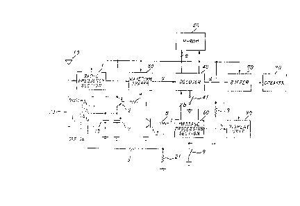
Referring to Fig. 6, a radio paging receiver
according to a first embodiment of this invention
operates when the receiver is supplied with electric
20 power from a power source 18, such as a battery. ~hen a
power supply switch 20 is turned ON, the electric power
is supplied from the bat-tery power supply or source 18
to every section of the radio paging receiver. A
capacitor 7 is connected in parallel to the battery
25 power supply 18. A desired radio frequency signal is
received and demodulated in a radio frequency section l
:,:
via an antenna 10. In a waveform shaping section 30, a
digital signal a as shown at the uppermost level in Fig.
.
J6;
64768-137
7 is provided. When the digital signal a is delivered to a
decoder ~0, the decoder 40 establtshes bit synchronization by
means of a preamble pattern P consisting of repetition of logic
signals "1" and "0", and then it turns to detection of a frame
synchronizing signal SC that is issued subsequently.
At this time, if detection of the frame synchronizing
signal SC is confirmed, the decoder 40 starts to read in paging
or calling number data from a P-ROM (programmable read-only
memory) 50 where its o~n paging number is preliminarily written.
The decoder 40 compares the paging number data with an address
~; signal A in the digital signal a bit by bit. If coincidence of
these data is confirmed, the decoder 40 activates a message
processing section 60 by means of a signal b (Fig. 6).
Subsequently, the decoder 40 carries out reception and decoding
of a subsequent message signal M, and waits for a stop signal
E. This operation flow is shown in Fig. 8.
The respective signals SC, A, M and E in Fig. 7 are
formed of BCH (Bose-Chaudhuri-Hocquenghem) codes of (31, 21)
known in the art. The frame synchronizing signal SC and the
stop signal E have fixed patterns, respectively. Each of the
address signal A and the message signal M has an MSB (most
signifieant bit~ in the information area of the BCH (31~ 21)
codes as an identification bit which is depieted in Fig. 7
along the bottom line labelled "A or M". If the identification
bit is a logic "0", the signal is processed as an address signal,
while if it is a logic "1", it is processed as a me~sage signal.
~ ~6~
64768-137
Here, the message data are formed by standard codes
of ISO (International Organization for Standardization) 7 bits,
and the message signal M is constructed by each ~CH (31, 21)
code having the information area of 20 bits in the manner
depicted in Fig. 7 along the bottom line.
Thus, if the stop signal E which indicates an end of
the message signal M is detected, calling indication means such
as a speaker 80 is made to sound via a buffer 70, and thereby
it notifies a possessor or holder of the radio paging receiver
that calling has been effected for him.
With the radio paging receiver in which a lot of
message data can be received and stored through the above-
mentioned procedure, a possessor of the radio paging receiver
can successively read out and confirm the message data stored
within the memory (that is, an external RA~ 300 in Fig. 9) in
the radio paging receiver by means of a read-out switch 9
according to necessity. Confirmation of the message data is
carried out by making a display unit 90 display the read-out
message data. The display unit 90 is, for example, an LCD
(liquid crystal display).
Now, the message processing section 60 and the display
unit 90 are explained in more detail in the following.
. ~
6~
Eirst, the message processing section 60 is
constructed as shown in Fig. 9, in which reference
numeral 100 designates a single chip CPU, numeral 200
designates a liquid crystal display (LCD) driver, and
5 numeral 300 designates an RAM. Furthermore, among these
components, a more detailed construction of the single
chip CPU is shown in Fig. 10, that of the LCD driver 200
is shown in Fig. 11 and that of the ~AM 300 is shown in
Fig. 12.
10In the single chip CPU 100 shown in Fig. 10,
; reference numerals 102 to 106 designate input ports,
numeral 107 designates an interrupt port, numeral 108
designates a serial interface, numerals 111 to 118
designate output ports, and numeral 120 designates a
15 data bus. Reference numeral 130 designates a program
counter for designating an address, numeral 140
designates a program memory in which a sequence of
instructions to be executed are stored and the contents
:
at the address designated by the program counter 130 are
20 read outO Reference numeral 150 designates an ALU
(Arithmetic and Logic Unit) for performing various
operations such as arithmetic operations and logic
operations, and numexal 160 designates an instruction
decoder for decoding information read out of the program
25 memory 140 to supply control signals corresponding to
the decoded instructions to the respective sections.
Reference numeral 170 designates an ACC (Accumulator) to
be used for transmission and reception of data between
:::
~;:
12
64768-137
a RAM 1~0 and the respective ports 104 to 119. Reference
numeral 180 designates the RAM to be used for memory of various
data, subroutines, program count in interruption, and saving of
a program status. Reference numeral 190 designates a system
clock generator for determining an executive instruction cycle
time.
In addition, in the LCD driver 200 shown in Fig. 11,
reference numeral 210 designates a column driver for performing
column control for the LCD, and numeral 220 designates a row
driver for performing row con-trol for the LCD~ Reference
numeral 230 designates an LCD voltage controller for controlling
a supply voltage to the LCD 90, and numeral 240 designates an
LCD timing controller for controlling drive timing of the LCD
90. Reference numeral 250 designates a data memory for
memori~ing display data fed from an output of a character
generator 290 or from a serial interface 295. Reference numeral
260 designates a system clock controller. A command decoder 270
takes in a command through the serial interface 295 and decodes
the command to control the respective sections in response to
the contents of the command. A data pointer 280 is for
designating an address for either writing data from the serial
interface 295 to the data memory 250 or reading data from the
data memorv 250 into the serial interface 295. Reference
numeral 290 designates the character generator for generating
a pattern based on a 7 x 5 dot matrix in response to the input
data, and numeral 295 designates the serial interface for
serially transferring data to and from the single chip CPU 100.
~ .
^`""'
:
13
~4768-137
In the external RAM 300 shown in Fig. 12, reference
numeral 310 designates a serial in-terface for transferring data
to and from the single chip CPU 100, and numeral 320 designates
an address counter. An X-~ decoder 330 analyzes data in the
address counter 320 and designates an address of a memory array
340 to write or read data in or from the memory. Reference
numeral 340 designates the memory array, and numeral 350
designates a control circuit.
When the signal shown at a in Fig. 7 is supplied to
the decoder 40 via the antenna 10, the radio frequency section
1, and the waveform shaping section 30 (Fig. 6), bit
synchronization is established at the portion P in Fig. 7 in
the decoder 40 and the operation shifts to detection of the
subsequent frame synchronizing signal SC. If a desired pattern
is transferred from the waveform shaping section 30 to a signal
detector circuit in the decoder 40, the pattern is compared
with the data fed from the P-ROM 50 bit by bit, and, at the
same time, detection of the stop signal is carried out.
Description will be made as regards receiving
operation of a message signal with reference to Fig. 10.
When a signal DET is supplied to the interrupt port
107 as a result of address coincidence, the single chip CPU 100
is excited via the interrupt port 107 and is supplied with a
clock CL corresponding to a transmission speed via the input
port 105. As a result, in the single chip CPU 100, the message
signal D is read in through the input port 106 in accordance
with the above mentioned clock CL. Predetermined contents of
14 ~ 3~ ``6
6~768-137
the program memory 140 are translated by the instruction
decoder 160, and processing of the message signal is carried
out in response to the respective commands. More particularly,
the above-referred read-in signal (that is, the message signal)
is written in a message storing area of the RAM 180 via the
data bus 120 and the ACC 170. Each time when 31 bits have been
received, operation is e-ffected in the ALU 150 to decode the
received signal. It is to be noted that the RAM 180 has also
a flag storing area for storing flags for the message signals
stored in the message storing area. When the message signal D
is stored in the message storing area, the flag for the stored
message signal is set into a logic "1".
Description will be made as regards the storing
operation of the message signal into the external RAM 300
with reference to Figs. 10 and 12.
In order to store and maintain 20 bits of the
information bits among the decoded respective BCH (31, 21)
codes, in the external RAM 300 as message information, the
single chip CPU 100 excites the external RAM 300 into an
operation mode by setting a chip enable signal line CE into a
logic "0" level. The
:: -
~2~
single chip CPU 100 provides the RAM 300 with addressinformation indicating what address of the RAM 300 the
message information is to be written in, via the serial
interface 108 and a signal line SOUT. At this time, the
5 single chip CPU 100 sends a system clock to the RAM 300
through a signal line SCK, and simultaneously sets a
signal line A/D into a logic "1" level in order to
represent that the information is an address. And at
this moment, in Fig. 12, the RAM 300 determines the
10 signal received through the signal line SOUT as an
address signal in accordance with the respective control
signals (CE, A/D, R/W), and an address of the memory
array 340 where the information is to be written is
designated via the address counter 320 and the X-Y
15 decoder 330.
Subsequently, in the single chip CPU 100,
message data to be written are sent out through a signal
line SOUT of the serial in~erface 108. At the same
time, the signal A/D is set into a logic "0" in order to
20 represent that the sent data are message data, and the
signal R/W is set into a logic "0" in order to represent
writing.
As a result, in the RAM 300 shown in Fig. 12, in
response to the respective control signals, the data
25 received through the signal line SOUT are written at the
previously designated address in the memory array 340
via the X-Y decoder 330, as message data.
~2~
16
64768-137
Description will be made as regards generating
operation of an alarm with reference to Figs. 6 and 10.
While the message signals are being decoded
successively through the above-mentioned procedure, when a
predetermined pattern representing an end of a message signal
is detected among the decoded message data or the message signal
cannot be received consecutively for 2 words, the single chip
CPU 100 notifies the decoder 40 that the message has ended, from
the output port 111 through a signal line ME. At -this moment,
the decoder 40 stops supply of the clock CL to the single chip
CPU 100.
In addition, when the decoder 40 has detected the
stop signal E, the decoder 40 stops supply of the clock CL to
the single chip CPU 100. Then, the single chip CPV 100
determines that the message signal has ended and stops decode
processing of the message signal. At the same time, a sound
generator circuit of the decoder 40 is controlled through the
output port 112 and a signal line AC. Thus, an alarm horn or
the spea~er 80 sounds, and thereby it is notified that calling
was done to the possessor.
Generally, a radio receiver of the type described has
a capability (auto-reset capability) of automatically stopping
the alarm sound after a predetermined period (for example,
about 8 seconds). In this preferred embodiment also~ a
frequency-divided output fT of an oscillator circuit in the
decoder 40 is applied to the input por-t 104 of the single chip
CPU 100, and this is used as a timing signal to control the
~::
~6¢) ~
17
64768-137
alarm sound for about 8 seconds.
Here it is to be noted that, during the alarm sound,
if a possessor of the radio paging receiver makes access to a
switch 41, a signal R is supplied from the decoder 40 to the
interrupt port 107 of the single chip CPU 100, hence supply of
a sound control signal AC from the output port 112 to the
decoder 40 is stopped without waiting for the lapse of 8
seconds, and so, the radio paging receiver stops the alarm
sound.
Simultaneously with the end of reception of the
; message signal, the decoded message data are displayed through
the following processes.
The single chip CPU 100 supplies first address
information of the corresponding message data to the external
RAM 300 through the signal line SOUT, also sets the chip enable
signal line CE into a logic "0" level and sets a chip select
signal line CS (this being a signal line for selecting the LCD
driver 200) and a signal line A/D into a logic "1" level.
Next, the single chip CPU 100 sets the signal line A/D into a
logic "0" level and also sets the signal line R/W into a logic
' level. Thereby, starting from the above-mentioned first
address, the corresponding data are successively read out bit
by bit from the memory array 340 via the X-Y decoder 330, and
the data are suppIied to the single chip CPU 100 via the serial
interface 310 and a signal line
: :::
18
SIN. When the data have been read out from the external
RA~ 300 in the above-described manner and have been
supplied to the single ch:ip CPU 100, the single chip CPU
100 shown in Fig. 10, at first sets the signal line CE
5 and a signal line C/D (C representing a command) into a
logic "1" level, and also in order to select the LCD
driver 200, it supplies a character transformation
command and storage address information to the LCD
driver 200 shown in Fig. 11 through the signal line SOUT
10 by setting the chip select signal line CS into a logic
"0" le~el. Subsequently, the single chip CPU 100
supplies the message data read out ~rom the external RAM
300 to the LCD driver 200 through the signal line SOUT
by setting the signal line C/D into a logic "0" level.
15 As described above, the RAM 180 stores a ~lag of a logic
"1" for the read-out message data. When the message
data is read out of the ROM 300, the CPU 100 carries out
operation to change the ~lag into a logic "0."
As a result, in the LCD driver 200 shown in Fig.
20 11, the co~mand decoder 270 decodes the information
subjected to serial-parallel conversion in the serial
inter~ace circuit 295 to produce an internal control
signal when the signal line C/D is set into a logic "1"
level. Here, i~ the command is either a ~rite command
25 or a character trans~ormation command, the data pointer
280 is accessed to set a write address therein.
On the other hand, i~ the signal line C/D is
given the logic "0" level, the data are delivered via
;
19
6~768-137
the serial interface 295 and are converted by the character
generator 290 into a pattern Eor a 7 x 5 dot matrix to be sent
as the signal C through the data memory 250 and the column
driver 210 and the row driver 220 to the LCD 90 under control
of the LCD timing controller 240. Thus, the pattern is
displayed on the LCD 90.
At this time, the display on the LCD 90 is scrolled
page by page.
Now, description will now be made, with reference to
Figs. 6, 9, and 10, as regards the case where a plurality of
messages are stored in the RAM 300, and among the stored
- messages there is an unconfirmed message which is not yet
confirmed by the possessor. In this case, in response to
memory contents, namely, the flags, in a predetermined area,
namely, the flag storing area, of the RAM 180 which monitors
unconfirmed messages and stores the flags as the monitoring
information, the single chip CPU 100 controls in such manner
that a PNP transistor 2 may be brought into a conducting state
by a drive signal via the output port 118, a resistor 5, an NPN
transistor 3 and a resistor 4, in contrast to the fact that
electric power was supplied from the battery 18 to the radio
paging receiver so far only through terminals Sl and S2.
- Accordingly, electric power is supplied from the battery 18
directly to the radio paging receiver through the transistor 2
regardless of the position of the switch 20, and therefore, even
if the possessor of the radio paging receiver should turn OFF
the switch 20 by mistake despite the fact that the unconfirmed
64768-137
messages are present within the RAM 300, the contents of the
RAM 300 can be protected.
In addition, when the switch 20 is turned OFF, the
voltage of the battery 18 is divided by resistors 6 and 21,
and the divided voltage is applied to the input port 103.
Thereby, the single chip CPU 100 confirms the logic "1" on
the port 103 and issues a predetermined alarm through the
output port 112. As a result, the possessor of the radio
paging receiver can recognize that an unconfirmed message is
present within the radio receiver, and can confirm the message
by reading. To stop the alarm, it is necessary to turn ON the
switch 20. For the confirmation operation, at first a read
switch 9 is operated and thereby unconfirmed messages within
the memory area are successively read out via the interrupt
port 107. The operation flow in such case where unconfirmed
messages are present, is shown in Fig. 13~
Description will now be made as regards a feature of
the radio paging receiver with reference to Figs. 6 to 10.
; As described above, the radio paging receiver is
~: 20 capable of responding to the message signal M specific to the
receiver when the receiver is supplied with electric power from
the power source 18. The receiver comprises the RAM 300
operable as a storing portion which is for
::
6~
storing the message signal M as a stored signal when the
storing portion is supplied with the electric power.
Responsive to the stored signal, a display unit of the
LCD 90 displays a display when the LCD 90 is supplied
5 with the electric power. The power supply switch 20 has
an on state and an of~ state and switches the electric
power to energize and deenergize the power source 18 in
the on state and the off state, respectively.
The CPU 100 having the RAM 180 is operable as a
10 monitoring portion which is coupled to the storing
portion and to the switch 20 and which monitors whether
or not the stored signal is delivered to the display
unit to produce a drive signal t (Figs. 6 and 10) after
the stored signal is stored in the storing portion until
15 the stored signal is delivered to the display unit. In
this event, the drive signal t is produced, with
reference to the flag storing area of the RAM 180, when
the flag storing area stores at least one flag of the
logic "1." When all flags stored in the RAM 180 are
20 changed into the logic "0," the CPU 100 stops production
; of the drive signal t.
A combination of the transistors 3 and 2 is
operable as a holding portion coupled to the switch 20J
the storing portion, and to the monitoring portion and
25 responsive to the drive signal for holding the electric
power to supply the electric power to the storing
portion an~ to the monitoring portion as long as the
~ drive signal is produced from the monitoring portion.
:'
~2~ 6
The speaker 80 is coupled to the monitoring
portion through the decoder 40 and the buffer 70, and to
the switch 20 through the resistance 6, the CPU 100, the
decoder 40, and the buffer 70. The speaker 80 is
5 operable as an alarm generating portion for generating
an alarm in response to the drive signal after the
switch 20 is put into the off state until the switch 20
is put into the on state.
Referring to Figs. 14 to 16~ a radio paging
10 receiver according to the second embodiment of this
invention comprises similar parts designated by like
reference numerals. The receiver has a circuit
construction in the case where a message protection
capability is provided by suppressing a consumed current
15 of the receiver small in a system that a drive voltage
for the message processing section and the subsequent
sections is higher than a drive voltage for the
preceding sections. The higher voltage is realized by
means of a booster circuit 88.
The operation of the receiver is as follows:
That is, a reception signal formed through an antenna
10, a radio frequency section 1 and a waveform shaping
~; circuit 30 is delivered to a decoder 42. The decoder 42
comprises a decoder memory 44. Then, in the decoder 42,
25 blt synchronization is established by a preamble signal
Pj and detection for a synchronizing signal SC is
effected. When the detection of the synchronizing
sig~nal has been confirmed~ the operation transfers to
:
~.
23
64768-137
detection of the received paging nu~lber (address number) A,
and it is sequentially compared with the contents of the P-ROM
50 where individual paging numbers are written. As a result,
if coincidence is confirmed therebetween, a message processing
section 61 is excited via a signal b, and the operation
transfers to decoding of message data M. The received message
data are once written in a RAM 300 of the message processing
section 61. If the reception of the message data M is finished,
message monitoring data, such as a flag representing whether or
not the message has been read out even once and the order of
reception, is written jointly with the message data in a
memory area of the decoder memory 44. Whenever the data within
the decoder memory 44 and the contents within the message
processing section 61 are different, the contents of the
decoder memory 44 are renewed. In Fig~ 16, it is sent to the
decoder memory 44 via the output port 119.
In addition, whenever reception of the message data M
is confirmed, a speaker ~30 is driven via a buffer 70 as is the
case with the receiver illus-trated in Fig. 6. Now, if a reset
switch 43 is depressed during driving of the speaker, it stops
the alarm. When it is depressed while the alarm is inoperative,
it acts as a message data read switch.
; The decoder 42 produces a drive signal t (Fig. 14)
having a logic 'IH'' level only when an unconfirmed message is
present among the received
:
"
~296~ i6
24
messages. Responsive to the drive signal t, a
transistor 3 is turned on. Therefore, a high voltage
system comprising the message processing section 61, the
display 90 and the booster circuit 88 is forcibly
5 brought into an operating state when the switch 20 comes
to an off state. The decoder 42 is coupled to the
switch 20 and produces an alarm signal AM (Fig. 16) only
when the switch 20 comes to an off state in the case
where the unconfirmed message is present among the
10 received messages. In this event, the decoder 42
judges, with reference to the contents of the decoder
memory 44, whether or not the unconfirmed message is
present. In order to issue an alarm in response to the
alarm signal "AM" in Fig. 16, the single chip CPU 100
15 controls the decoder 42 via an alarm control terminal
"AC" so as to drive the speaker 80 via the buffer 70 and
thereby notifies the possessor of the radio paging
receiver that the unconfirmed message is present.
Here, a circuit formed of a capacitor 11, a
20 diode 13 and a transistor 14 is a circuit for quickly
discharging the charge on the capacitor 12 connected to
the output voltage terminals of the booster circuit 88
to make the initial reset of the message processing
sec*ion 61 correctly operable.
As mentioned above, the decoder 42 having a
decoder memory 44 is operable as a monitoring portion
which is coupled to the storing portion 300 and to the
switch 20 and which monitors whether or not a stored
signal (that is, a message signal) stored in the storing
portion is delivered to the display unit 90 to produce a
drive signal t after the stored signal is stored in the
storing portion until the stored signal i5 delivered to
5 the display unit.
A combination of the transistor 3, the booster
circuit 88, and a ground lead 100 (Fig. 14) connected to
a terminal S2 of the switch 20 is operable as a holding
portion coupled to the switch 20, the storing portion
10 300~ and to the monitoring portion and responsive to the
drive signal for holding the electric power to supply
the electric power to the storing portion and to the
monitoring portion as long as the drive signal is
produced fr~m the monitoring portion.
The speaker 80 is coupled to the monitoring
portion through the buffer 70 and to the switch 20
through the buffer 70 and the decoder 42, and generates
an alarm in response to the drive signal after the
switch 20 is put into the off state until the switch 20
20 is put into the on state.
As explained above, according to the present
invention, there are advantages that unconfirmed
messages would not be lost by erroneous operation of a
power supply sw1tch of a radio paging receiver and also
25 that fact can be notified to the possessor of a radio
paging receiver.
While this invention has thus far been described
; in conjunction with a few embodiment thereof, it will
26
readily be possible for those skilled in the art to put
this invention into practice in various other manners.
For example, the power supply swi-tch 20 may be a slide
switch 21 (Fig. 4) having a depressing function.
5 Alternatively, the power supply switch 20 may be formed
of a single electronic switching circuit element which
can be selectively put into an on state and an off
state.