Note: Descriptions are shown in the official language in which they were submitted.
~2~ 2
1 20355-2~96
Siemens Aktiengesellschaft
Method and arrangement for generating a correction
signal for a digi~al timing recovery device.
The invention relates to a method for generating a
correction signal in a digital timing recovery device upon
reaching a de~ined phase spacing between a digital signal and a
first data auxiliary clock pulse associated therewith which
represents a selection changing with the phase spacing of one of
several auxiliary clock pulses having the same frequency, which is
somewhat greater or smaller than the bit rate of the digital
signal, and having the same phase spacing between each other.
A method of this kind is the basis of two earlier
proposals. According ~o a first one a phase sensor outputs a
correction signal when the effective edge of the data auxiliary
cloak pulse approaahes an edge of the digital signal at less than
a fixed time interval. Eor this purpose it requires a delay
deviae. In the seaond one the correction signal is obtained whqn
the effective flanks of the digital signal match a special clock
pul~e likewise derived from an auxiliary clock pulse and having
the same frequency as the data auxiliary clock pulse and displaced
with respect to the latter by a certain value in the phase.
The objeat of the invention is to disclose a method
which can be xeali~ed without a delay device and also without a
special c~ock pulse and which can hence be carried out in
integrated circuit teahnology also for bit rates equal to or
greater than 34 ~bit/s.
~ '~
~9¢~ l~
2 20365-2896
Starting from a method of the type described in the
introduction, this object is achieved in that the data auxiliary
clock pulse is sampled with the leading edge of the pulse of the
cligital signal until an edge of a selected edge type of the data
auxiliary clock pulse is detected by means of a change in state
during the sampling, and in that the correction signal i5 then
triggered. Eclge types are either leading or trailing edges.
It is advantageous if the sampling is blocked for the
duration of the correction signal.
It is furthermore advantageous if a symmetrical pulse is
selected as the first data auxiliary clock pulse and if, for the
detection, the edge type where the edges have the defined phase
spacing of 0.5 UI (Unit Interval) is selected.
The defined phase spacing or the fixed time interval is
used as a gauge, the measured phase spacing or time interval
between the effective edges of the data auxiliary clock pulse and
the leading edges of the pulses of the digital signal continuously
changing in a define range. When the measured spacing reaches the
gauge, the correction signal is triggered.
According to a broad aspect of the invention there is
provided a method for generating a correction signal (K) in a
digital clock recovery means upon attainment of a defined phase
spaclng between a digital signal DSli, DS2a, DS2b and a first
auxiliary data clock (DHT1~ alloca~ed thereto, the first auxiliary
data lock being selected from a plurality of auxiliary clocks the
selection of which changes with the phase spacing, said auxiliary
clocks having the same frequency which is somewhat higher or lower
,~
2a 20365-2896
than ~he bit rate of the ~igital signal and having identical phase
spacing relative to one another, eomprislng sampling the auxiliary
data clock (DHT1) with the leading edge of the pulses of the
digital signal until an edge of a selected edge type of the
auxiliary data clock (DHT1) is identified by a status change in
the samples; and then releasing the correction signal (K).
According to another broad aspeet of the invention there
is provided a phase sensor having an output which provides a
correction signal (K) ~omprising a first sample-and-hold circuit
having a first digital signal input and having a first auxiliary
data clock input and a means for generating the correction signal
~K), said means for generating having an input connected to an
output of said first sample-and-hold circuit, a first D-flipflop
being said first sample~and-hold circuit, a D-input o~ said first
D-flipflop being connected to the first auxiliary data clock input
and a clock input thereof being connected to the first digital
signal input, a Q output thereof being the output of said first
sample-and-hold circuit.
The invention will be explained in more detail with
re~erence to exemplary embodiments.
Figure 1 shows a block circuit diagram of the phase
sensor according to the invention for a binary digital signal,
Figure 2 shows a pulse diagram for explaining the
function of the phase sensor aceording to Figure 1,
~ igure 3 shows a bloek eircuit diayram of the phase
sensor according to the invention for a bipolar digital signal,
~ ~.
7~
2b 20365-2896
Figure 4 shows the block circui-t diagram of a
commercially available D flip-flop with test inputs and
Figure 5 shows in detail a first phase sensor according
to the invention,
Figure 6 shows a pulse diagram for explaining the first
phase sensor,
Figure 7 shows in detail a second phase sensor according
to the invention and
Figure 8 shows a pulse diagram for explaining the second
phase sensor.
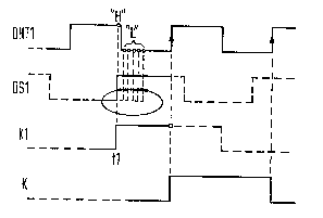
Figure 1 shows a phase sensor according to the invention
for a binary digital signal DSl with a sample and hold circuit 3
and a device 6 for generating the correction signal K. Figure 2
shows the associated
~ 2
puLses. --3~
The leading edges of the digital signal DS1 at
input 1 move depending on the sign of the frequency
deviation with respect to the data auxiliary clock pulse
DHT1 at input 2 from clock pulse period to clock pulse
period either only to the left or only to the right of
these selected trailing edgesu In Figure 2 they move
only to the right, as is indicated by dashes, until the
present phase position represented by a solid line is
10 reached. In each clock pulse period, the data auxiliary
clock pulse DHT1 is sampled with the leading effective
edge of the pulses of the digital signal DS1. ~y evalua-
ting the samples, the trailing edge of the data auxi-
liary clock pulse DHT1 is detected. Upon detection of
15 the state change of the samples at time t1, a correction
request s;gnal K1 is generated at connection ~. The
favourable phase spacing of 0.5 UI bet~een the effective
leading edges of the data auxiliary clock pulse DHT1 and
the leading edge of the pulses of the digital signal DS1
ZO is obtained from the spacing between the trailing and
the leading edge of a period of the data auxiliary clock
pulse DHT1. The symmetry of the data auxiliary clock
pulse DHT1 must be great for the required position.
This can be real;~ed for the most part independently of
25 the tolerances. In the device 6, the correct;on signal
K is generated at output 7 synchronously to the data
auxiliary clock pulse DHT1.
In contrast to the second earlier proposal, this
is achieved ~ithout a special clock pulse derived from
30 the auxil;ary clock pulse.
Fi~ure 3 shows a phase sensor according to the
invention for a bipolar digital signal with the half-
waves DS2a and DS2b. The first half-wave DS2a is suP-
plied to the sample and hold c;rcuit 3. A further
35 sample and hold c;rcuit 10 is introduced ~or the second
half-wave DS2b. The device 6a for generat;ng the correc-
tion signal K has two inputs for the correction request
signals K1 and K2 from both sample and hold circuits 3
and 10. It carries out an OR operation on both correc-
~6~
~,
tion request signals K1 and K2.
Figure 4 shows the block circuit diagram of acommercially available D flip-flop with test inputs.
~esides the D flip-flop 16, it contains an inverter 12,
AND gates 13 and 14 and an OR gate 15.
6esides a D input, a clock pulse input CP, 3
reset input R and a Q output and a Q output, a test
input TI and a test enable input TE are provided.
Figure 5 shows in detail a phase sensor accor-
10 ding to the invention which can be used in a timingrecovery device working with negative frequency devia-
tion. The circuit part ~ith the solid lines is required
for a binary digital signal DS1. For a bipolar digital
signal DS2a, DS2b, ~he circuit part with the dashed
15 lines is additionally required. The arrangement con-
sists of sample and hold circuits with simple D flip-
flops 3a and 10a and a device 6a1 for generating the
correction signal K. The latter contains a first stage
with a NAND gaee 17a and a D flip-flop with test inputs
20 18, a second stage with a D flip-flop with test inputs
19 and a reset stage with an AND gate 20.
The phase sensor realized ~ith digital integra-
ted D flip-flop cells ~orks under special conditions.
For the reliable switching of a D flip-flop, it must be
25 ensured that the signal at the D input is not subjected
to a change in state during the declocking. Otherwise
instable s~;tching operations could result, the initial
state of the D flip-flop then being undefinable. A
metastable state ~ould then arise. However, since the
30 phase sensor serves specifically to detect a change in
the data auxiliary clock pulse DHT1~ the probability of
the occurrence of unstable switching operations is
therefore relatively h;gh. This means that the correc-
tion request signal K1 can often become unstable. Meta-
35 stabLe states can, hnwever, be suppressed by a multi-
stage sampling of the correction request signal K1.
This is realized in t~o stages in the synchronous gene-
ration of the correction s;gna~ K by means of the D
flip-flop ~ith test inputs 18 and 19. Both the genera-
-- 5tion of the correction signal K as ~ell as the resetting
are synchronous to the data auxiliary clock pulse DHT1.
How this phase sensor works will be explained
below also ~ith reference to the pulse diagram in Fig. 6:
S The setting signal E at input 21 with the logical "L"
state sets all D flip-flops 3a, 10a, 18 and 19 to their
initial state. The Q outputs of the D flip-flops 18 and
19 as well as the output of the AND gate 20 receives the
logical "L" state. Follo~ing this, the Q outputs of the D
10 flip-flops 3a and 10a assume the logical "H" state and
finally the output of the NAN3 gate 17a assumes the
logical "L" state. Via the feedback from the Q output
of the D flip-flop 19 to the TE inputs of the D flip-
flops 18 and 19, the latter are switched to D mode.
15 This state remains unchanged as long as the sampling
vaLues have the logical "L" state. This corresponds to
a logical "H" state at the Q output of the D flip-flop
3a. If, on the other hand, the sampling value has the
logical "H" (t1) state and accordingly the Q output
20 has the logical "L" state~ then this means a correction
request signal K1. The latter is read into the D flip-
flop 18 as a precorrection signal K at instant t2
with the here effective leading edge of the clata auxi-
liary clock pulse DHT1 via the NAND gate 17a. If this
25 reading-in operation was execu~ed in a stable manner,
then in the next period of the data auxiliary clock
pulse DHT1 a synchronous correction signal K is genera-
ted (t3) by means of the precorrection signal K from
the D flip-flop 19 at ~he ~ output. Otherwise this does
30 not take place. The correction signal K with the
logical state "H" simultaneously switches the D flip-
flops 18 and 19 over to the test inputs TI~ which ~ere
moved to the logical "L" state via the input Z2, in
order to switch off the correction signal K at instant
35 t4 in the subsequen~ period of the data auxiliary
clock pulse DHT1~ The correction signal K triggers at
instant t3 a s~itch-over US in the auxiliary clock
pulses, the effective edge of the next DHT period being
displaced forwards by the s~itch-over ~ith the phase
:
-- 6
spacing of the auxiliary clock pulses at instant t4 and
hence a phase correction being created. During the gen-
eration of the correction signal K (between instants t2
and t4), the Q outputs of the D flip-flops 18 and 19 block
a further sampling via the AND gate 20. At instant ts,
the phase sensor can again monitor the phase position of
the digita( signaL DS1 with respect to DHT1 by means of
sampling.
On a bipolar digital signal DS2a, D52b is sup-
plied to the inputs 1 and 8, the correction signal K canbe generated both by the correction request signal K1
and from the correction request signal K2.
Fig. 7 shors a two-stage "bisynchronous" phase
sensor for a timing recovery device working with posi-
tive frequency deviation. Bisynchronous ~eans that thecorrection signal K for producing a delay equalization
for the switch-over is generated synchronously to a
second derived data auxiliary clock pulse DHT2, the
sample and hold circuit 3a and 10a and the reset stage
26 to 30 fixedly connected thereto continue to run syn-
chronously to the data auxiliary clock pulse DHT1.
The arrangement contains a D flip-flop 3a as the
sample and hold circuit and, in the case of a processing
of bipolar digital signals, additionally a D flip-flop
10a. The rest of the circuit is a device 6a2 for gene-
rating the correction signal K. This device contains a
first stage with a NAND gate 17 and a D flip-flop 23~ a
second stage w;th a D flip-flop with test inputs 24 and
a reset stage with an inverter 27, with NAND gates 26
and 29, ~ith an 0~ gate 28, with an NOR gate 30 and with
a D flip-flop 25. The way this arrangement ~orks is
also evident from the pulse diagram in F;gure 8.
The setting signal E `causes with its logical "L"
state the device 6a2 to return to ;ts initial state~ in
that all D flip-flops 3a, 23, 24 and 25 are reset either
directly or via the gates. The binary digital signal
DS1 is applied to the digital signal input 1 and to the
data auxiliary clock pulse input 2 of the data auxiliary
cLock pulse DHT1. In the D ~lip-flop 3a, the data auxi-
~ 7 ~
liary clock pulse D~T1 is then sampled with the digital
signal 351. If the ~ output assumes a logical "L" state
during the sampling, then this means a correction
request signal K1 (t1). After the reset via the S
input, the Q output switches to a logical "H" state.
If half-waves of a bipolar digital signal DS2a
and DS2b are present at the digital signal inputs 1 and
8, then a further correction request signal K2 can be
generated by the D flip-flop 1~a. If in the first stage
10 one of the two inputs of the NAND gate 17 then assumes a
logical "L" state, then the D input of the D flip-flop
23 receives a logical "H" state. If this operation was
executed in a stable manner, this state is read in (t2)
with the data auxiliary clock pulse DHT2, which has a
15 fixed phase spacing with respect to the data auxiliary
clock pulse DHT1, as a precorrection signal K . This
precorrection signal K can be used favourably for the
preparation of the switch-over assuming that a meta-
stable operation in this signal cannot cause an incorrect
20 control. In the subseguent period of the data auxiliary
clock pulse DHT2, this logical "H" state is read in
further at instant t3 into the D flip-flop 24 of the
second stage and the correction signal K arises there at
the Q output thereof. This triggers the s~itch-over US,
25 the effect;ve edges of both data auxiliary clock pulses
HT1 and DHT2 being displaced backwards ~ith the phase
spacing of the auxiliary clock pulses, so that at
instant t4 this logical "H" state is read in further
Vi3 the data auxiliary clock pulse DHT1 into the D flip-
30 flop 25 of the reset stage and the Q output thereoflikewise receives the logical "H" state as a reset signal
R ~ After the trailing edge of the data auxiliary
clock pulse DHT1 (tS~, the D flip-flop 24 is reset via
the gate combination 26, 28 and 29 and the reset input
35 and hence the correction signal K is terminated~
The D flip-flops 3a, 10a and 23 are reset via
the correction signal K by the reset signal R and
blocked until the ~ output of the D tlip-flop 25 again
assumes a logical "L" state with the data auxiliary
~Z5~7~
-- 8
clock pulse DHT1 at instant t6. At instant t7, the
phase position of the digital signal DS1 is again moni-
tored.
With the introduction of the second data auxi-
liary clock pulse DHT2, the phase spacing of which tothe data auxiliary clock pulse DHT1 can be variably
selected for matching the delays, the probability of the
occurrence of metastable states at the precorrection
signal K may in some circumstances increase. As a
10 result of using a D flip~flop 24 with test inputs in the
second stage, however, the instance of such states on
the correction signal K can be avoided.
Both phase sensors can be real;zed and integra-
ted HCMOS technology for bit rates > 34 Mbit/s.
12 Patent claims
8 Figures