Note: Descriptions are shown in the official language in which they were submitted.
83-406
--2--
BACKGROUND OF T~E INVENTION
1. Field of the Invention
The invention relates generally to the field of digital
data processing systems and more specifically to systems for
marking as stale entries in processor cache memory circuits
which include data for which the data stored in main memory
has been overwritten by other units in the system.
2. Description of the Prior Art
A typical digital data processing system includes three
basic elements, namely a processor element, a memory
element, and an input/output element. The memory elemen~
stored information in addressable storage locations. This
information includes both data and instructions for
processing the data. The processor element includes one or
more digital data processing units, or "processorsn, each of
which causes information to be transferred, or fetched, to
it from the memory element, interprets the incoming
information as either instructions or data, and processes
the data in accordance with the instructions. The results
$~r,~
83-406
--3--
are then stored in addressed locations in the memory
element.
The input/output element also communicates with thé
memory element in order to transfer information into the
system and to obtain the processed data from it. Units
comprising the input/output element normally operate in
accordance with control information supplied to it by the
processor element. The control information defines the
operation to be performed by the input/output unit. At
least one class of operations performed by an input/output
unit is the transfer of user information, that is,
information used by a user program, between the input/output
unit and the memory element. Typical units comprising the
input/output element include, for example, printers,
teletypewriters, and video display terminals, and may also
include secondary information storage devices such as disk
or tape 6torage units.
In addition to functioning as input/output devices,
disk storage units and, under some circumstances, tape
storage units may also function as part of the memory
element. In particular, a memory element typically includes
&,lQ6
83-406
--4--
a main memory, whose contents are accessible to the
processor relatively quickly but which i5 generally
relatively high-cost storage. Modern main memories are
typically implemented using MOS or bipolar ~emiconductor
technology and may provide on the order of a fraction of a
megabyte to several tens of megabytes of storage.
On the other hand, the time required to access
information stored in disk storage units is much longer than
main memory, but the disk units can provide large amounts of
storage, on the order of hundreds of megabyte~ or more, at
relatively low cost. In addition, unlike main memory, disk
storage is non-volatile, that is, the information is not
lost if power is removed. Therefore, disk units are used to
provide backup storage for the main memory, that is, to
provide storage for information which will not fit into main
memory until a program needs it. When a program requires
information which is stored on a disk but is not in the main
memory, that information is transferred into the main
memory. If necessary, the contents of the locations in the
main memory into which the information from the disk unit
was transferred may be transferred to a disk unit for
storage therein before being overwritten by data from the
disk.
12~6~6
83-406
--5--
In many digital data processing systems, the processor
(assuming only one processor), mass storage devices and
other input/output devices all communicate with a single
main memory or only a few main memory modules. This may
produce contention for the main memory which can interfere
with the processor's ability to quickly obtain information
from the main memory. This, in turn, can slow the
processor's ability to execute programs. The contention
problem is exacerbated if all of the units are connected to
a single input/output bus, as all information that is
transferred must be transferred over the single bus.
Accordingly, in many modern computer systems, the
processor includes a cache memory, which is a small private
memory accessible only to the processor which stores
information from the most recently-requested locations in
main memory and from nearby locations. In typical data
processing systems, when the processor requests an item of
information from a location in the main memory, it will
oftentimes require the contents of adjacent locations
shortly thereafter. Accordingly, when the processor is able
to request information from the main memory, it requests
83-406
--6--
more than it needs at that immediate time, with the
expectation that it will likely need at least some of the
remaining information shortly thereafter. When the
processor gets the item information it then needs, it can
immediately begin using it, and if it turns out that the the
processor can use the other information that was received,
it will have that information stored in the cache, and will
not have to wait until it is obtained from the main memory.
Typically a cache memory is organized into blocks each
capable of storing a predetermined amount of information.
When information has been retrieved from main memory and
loaded into a cache block, that block is assigned ~n
address, termed a "tag". The tag corresponds to the address
of the corresponding locations in main memory from which the
information was retrieved; thus the blocks of the cache are
identified with the locations in the main memory. When the
processor requires information, the tags in the cache can be
examined to determine whether a block contains the requested
information. If one does, the information is obtained from
the cache; otherwise, the processor retrieves the
information from the main memory.
106
83-406
--7--
As has been mentioned, when a disk unit transfers
information to the main memory, it may overwrite information
which was previously in the main memory. When that occurs,
however, if information has been stored in one or more
blocks in the cache from those locations in main memory, the
information in those blocks is stale, that is, the blocks do
not contain copies of the information in the memory.
SUMMARY OF THE INVENTION
The invention provides a new and improved mechanism for
marking as stale blocks in a cache memory so as to indicate
that the contents of the main memory associated with those
blocks have been changed since the information was stored in
the cache.
In brief summary, a digital data processing system
includes a processor including a cache memory controlled by
a bus interface CilCUit. The processor communicates with a
main memory and one or more secondary information storage
units over a common bus. The bus includes lines for
transferring addresses and information, an address strobe
signal identifying when addresses are being transferred, and
~Z~
- 8 - 60412-1795
a line for transferring a cache control signal. If the cache
control signal is asserted immediately prior to the transfer of
the address over the address lines and the assertion of the
address strobe signal, the bus control circuit compares the
address with the addresses associated with the contents of the
cache memory. If a block in the cache memory is associated with
the address transferred, the bus control circuit marks as stale
the contents of the cache block. A second block, which is
associated with main memory locations adjacent the block just
marked stale may also be marked stale if the cache control signal
is associated a second time while the address strobe signal is
asserted.
The invention may be summarized, according to one
aspect, as a unit for connection to a bus in a digital data pro-
cessing system including at least one other unit connected to said
bus, the unit including a cache memory having a plurality of
entries each comprising a block, a tag store and a stale indicator
having a valid condition and a stale condition, said unit further
including bus interface circuit for connection to said bus for
receiving address signals, an address control signal having an
asserted condition and a negated condition, and a cache control
signal having an asserted condition and a negated condition over
respective lines of said bus, said bus interface circuit further
being connected to said cache memory means and including: A. an
address receiving circuit connected to said bus responsive to said
address control signal for receiving said address signals, B. a
~2~J~ 6
- 8a - 60412-1795
tag comparator connected to said address receiving circuit and aLl
of said tag stores for determining if a correspondence exists
between said address signals and the contents of said tag stores
in response to the receipt of a first cache control signal and
between incremented address signals and the con-tents of said tag
stores in response to the receipt of a second cache control sig-
nal; and C. a stale indicator conditioning circuit connected to
said tag comparator and said bus responsive to the receipt of said
cache control signal and a positive correspondence for condition-
ing the stale indicator of -the entry having the positive corres-
pondence to said condition.
BRIEF DESCRIPTION OF THE DRAWINGS
This invention is pointed out with particularity in the
appended claims. The above and further advantages of this inven-
tion may be better understood by referring to the following des-
cription taken in conjunction with the accompanying drawings, in
which:
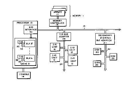
Fig. 1 is a block diagram of a digital data processing
system constructed in accordance with the invention;
~2~ 6
83-406
_g_
Fig. 2 is a diagram depicting various lines of a bus
which is used in connecting various units in the system
depicted in Fig. 1
Fig. 3, comprising Figs. 3A and 3B, includes timing
diagrams useful in understanding the operation of the system
depicted in Fig. 1.
DETAILED DESCRIPTION OF AN ILLUSTRATIVE EMBODIMENT
Referring to Fig. 1, a data processing system including
the invention includes, as basic elements, a processor 10, a
memory 11 and one or more input/output units 12. A bus 13
interconnects the processor 10, memory 11 and input/output
units 12 in parallel. The processor 10 executes
instructions that are stored in addressable storage
locations in the memory unit 11. The instructions identify
operations that are to be performed on operands, which are
also stored in addressable locations in the memory unit.
The instructions and operands are fetched by the processor
10 as they are needed, and processed data are returned for
storage in the memory 11. The processor lO also transmits
1~6~06
83-406
--10--
control information to the input/output units 12, enabling
them to perform selected operations, such as transmitting
data to or retrieving data from the memory 11. Such data
may include instructions or operands which may be
transmitted to the memory 11 or processed data which is
retrieved from the memory 11 for storage or display.
An operators console 14 serves as the operator's
interface. It allows the operator to examine and deposit
data, halt the operation of the processor 10 or step the
processor 10 through a sequence of instructions and
determine the responses of the processor 10 in response
thereto. It also enables an operator to initialize the
system through a boot strap procedure, and perform various
diagnostic tests on the entire data processing system.
The memory 11 includes a memory controller 15, which is
connected directly to the bus 13 and to a plurality of
arrays 17. The arrays 17 contain a plurality of addressable
storage location in which information is stored. The memory
controller 15 receives transfer requests from the processor
10 or from an input/output unit 12 over the bus 13. The
memory controller 15 may receive several types of transfer
83-406
requests over bus 13, which fall into two general
categories. In one category, information is written into,
or stored in, a storage location, and in the other category,
information is retrieved, or read, from a storage location.
The data processing system may include several types of
input/output units 12, including disk and tape secondary
storage units, teletypewriters, video display terminals,
line printers, telephone and computer network units, and the
like. All of these units communicate with the bus 13 over a
device bus through one or more bus adapters. As shown in
Fig. 1, the disk drives 20 are connected to a secondary
storage bus adapter 21 over a device bus 22. The secondary
storage bus adapter 21 is, in turn is connected to bus 13.
Others of input/output units 12 are connected to an
input/output bus adapter 25 over a device bus 24.
Transfers by the processor 10 over bus 13 are
controlled by a bus interface circuit 30. The bus interface
circuit 30 transmits and receives signals, as described in
part below in connection with Fig. 2, which, at the request
of the processor's processing circuits (not shown) effect a
transfer of information over bus 13 with the other units
06
83-406
-12-
connected thereto. The bus interface circuit 30 also
controls a cache memory 31, storing information therein
received from the memory unit 11 over bus 13. In addition,
if the processing circuits have requested information which
is stored in the cache memory 31, the bus interface circuit
30 retrieves the information and transfers it to the
processing circuits.
Cache memory 31 is a conventional information storage
circuit in a processor 10. Cache memories are described in
K. Hwang and F. Briggs, Computer Archi~ecture ~nd Parallel
Processing (McGraw-Hill, 1984), Section 2.4, pp. 98, et seq,
and V. Hamacher, Computer Organization (McGraw-Hill, 1984),
Section 8.6, pp. 306, et seq. Cache memory 31 includes a
plurality of storage locations organized into blocks, with
each block containing two storage locations. Each storage
location stores one word of information, t~hat is, the amount
of information which may be transferred over bus 13 at one
time. In one specific embodiment, a word of information
corresponds to four bytes, or thirty-two binary digits, of
information. ~hus, a block includes storage locations for
eight bytes of information.
~3-406
-13-
As will be appreciated by those skilled in the art, the
information stored in a block in the cache memory 31, when
it is received from the memory unit 11, is a copy of the
information stored in the memory unit 11. Each block in the
cache memory 31 has an associated tag 32 whose contents are
established by the bus interface circuit 30 ts identify the
locations in the memory unit 11 from which the information
was copied. In addition, each block includes a stale flag
33 which is reset or cleared by the bus interface circuit to
indicate whether or not the contents of the block are in
fact copies of the locations identified by the ~ag, that is,
whether or not the contents of the block are stale.
Circumstances under which the contents of a block may
be marked stale are well known. At least one such
circumstance is when another unit connected to bus 13
transfers information to memory unit 11 for storage in a
location whose contents have previously been copied into a
block in the cache memory 31. If that occurs, the contents
of the block in the cache memory 31 are "stale", that is,
they no longer correspond to the contents of the locations
in memory unit 11, and so the processor 10 cannot use the
information in that block of the cache memory 31. In the
83-406
-14-
above-described embodiment in which a cache block has two
storage locations, if the contents of either location do not
correspond to the contents of the corresponding location in
memory, that block is marked stale.
~ us 13 includes a plurality of lines for carrying
signals among the various units connected thereto. It will
be appreciated that each of the units includes circuits (not
shown) for either receiving and using, or transmitting, some
or all of the signals. Fig. 2 depicts a number of the lines
comprising one embodiment of bus 13.
With reference to Fig. 2, bus 13 include a ~et of
data/address lines ("DAL" ) 35 over which a commanding unit
transmits signals representing information and transfer
command/address are transferred. In bus 13, the transfer
command signals, that is, the signals identifying the number
of words to be transferred in response to the command, are
transferred with the address. Only one address is
transferred even if more than one word of information is to
be transferred; if more than one word is to be transferred
in response to the command, the first word is associated
with the location identified by the address, and additional
?6
83-406
-15-
words are taken from locations identified by successive
Addresses .
After the commanding unit has placed address signals on
the data/address lines 35 and allowed them to settle and
deskew, it transmits an asserted AS address strobe signal
over a line 36. Other units may use the asserted AS address
strobe signal to strobe in, and use, the address signals.
If the unit transmitting the address also transmits a WR
write signal over a line 37 to enable a WRITE operation,
that is a transfer of information to the location identified
by the address just transmitted. A predetermined time after
asserting the AS address strobe signal, the commanding unit
removes the command and address signals from the
data/address lines 35 and places information siqnals
thereon. A selected time later, after the information
signals have been allowed to settle and deskew, the unit
transmits an asserted DS data strobe signal over a line 40,
enabling the unit containing the addressed location, that
is, the responding unit, to receive the data and store the
information in the addressed location. The responding unit
then transmits an asserted RDY ready signal over a line 41,
which is received by the transmitting unit. The DS data
P~i ~l(P6
83-406
-16-
strobe and AS address strobe signals are then negated. The
responding unit then negates the RDY ready signal.
If, on the other hand, the commanding unit, that is,
the unit which transmitted the address signals on the
data/address lines, does not assert the WR write signal, a
read operation is enabled in which the responding unit
transmits the information stored in that location over the
data/address lines 35. In particular, the commanding unit,
removes the address signals at some time after the AS
address strobe signal has been asserted, and asserts the DS
data strobe signal. The responding unit then places the
information signals from the location identified by the
address on the data/address lines 35, and asserts the RDY
ready signal. In response, the commanding unit strobes the
signals on the data/address lines 35, negates the DS data
strobe and AS address strobe signals and the responding unit
negates the RDY ready signal.
As has been described above, multiple words of
information may be transferred over bus 13 in response to a
single address. This is accommodated by the commanding unit
maintaining the AS address strobe signal asserted, and, for
83-406
-17-
each word to be transferred, asserting the DS data strobe
signal. If the operation is a WRITE operation, the
commanding unit transmits a new information word for each
asserted DS data strobe signal, and the receiving unit
asserts the RDY ready signal in response the}eto. After the
receiving unit negates the ready RDY signal, the commanding
unit may transmit a new information word and assert the DS
data strobe signal.
If the operation i6 a READ operation, after the
commanding unit transmits the DS data strobe signal, the
receiving unit places a new information word onto the
data/address lines 35 and asserts the RDY signal. After the
receiving unit negates the RDY signal, the commanding unit
may again assert the DS data strobe siganl.
A commanding unit may be any unit which initiates
transfers to or from the memory unit. In the digital data
processing system depicted in Fig. 1, the processor 10 and
secondary storage bus adapter 21 initiate transfers with
memory unit 11. In addition, under some circumstances,
input/output bus adapter 25 may also initiate transfers with
memory unit 11. Adapters 21 and 25 thus have direct access
83-406
-18-
to memory unit 11, that is, they engage in "direct memory
access", or "DMA", transfers. If either adapter 21 or 25
wish to make DMA transfers with memory, they engage in an
arbitration operation in which processor 10 determines
whether a D~ transfer should take place. The unit wishing
to make a DMA transfer transmits an asserted DMR direct
memory request signal over a line 42; in response, the
proceEsor 10 asserts a DMG direct memory grant signal over a
line 43. The unit receiving the DMG direct memory grant
signal may then become the commanding unit on bus 13.
In addition to the above-described signals, bus 13
includes a number of lines 44 for carrying signals by which
other units in the system can request interrupt service or
otherwise signal the occurrence of unusual events, and other
lines 45 for carrying miscellaneous control and timing
signals.
Furthermore, in accordance with the invention, the bus
13 includes a line 46 for carrying a CCTL cache control
signal which may be asserted by a commanding unit during a
DMA transfer, that is, a unit such as adapters 21 or 25
which transfer information signals to memory unit 11
83-406
-19-
directly over bus 13. The commanding unit uses the CCTL
cache control signal in conjunction with signals transmitted
over other lines of the bus 13 to enable bus interface
circuit 30 to (a) determine whether the contents of the
addressed location identified by the address signals over
the data/address lines 35 have been copied into a block in
the cache memory 31 by comparing the address signals to the
contents of the tags 32, and, (b) if there is a
correspondence between the address signals and the cache
tags 32, that is, if they have been copied into a block, set
the stale flag 33 of that block to indicate that the
corresponding location in memory unit 11 has been
overwritten. While the bus interface circuit 30 is
performing these operations, the commanding unit and the
addressed unit may continue with an information transfer
over the bus 13 using the data/address lines 35 and the DS
data strobe signal as described above. ~hus, by asserting
the CCTL cache control signal if the information being
transferred is information which normally could have been
loaded into the cache, in conjunction with the other signals
on bus 13, the commanding unit is able to both initiate an
information transfer over the bus 13, and also enable the
bus interface circuit 30 to perform the operations described
61()6
B3-406
-20-
above.
Fiqs. 3A and 3B depict the timings for the various
signals, including the CCTL cache control signal on line 46
~Fig. 2). Fig. 3A depicts the timing related to a transfer
in which one block of a cache may be marked stale, and
Fiq. 3L depicts the timing related to a transfer in which
multiple blocks may be marked stale. As described above, a
commanding unit may effectuate information transfers with
multiple storage locations in response to a single address
transfer by maintaining the AS address strobe signal
asserted. If this occurs, the bus interface circuit 30 may
have to mark multiple blocks of the cache memory 31 (Fig. 1)
stale.
With reference to Fig. 3A, the CCTL cache control
signal is asserted by the commanding unit before it places
the address signals onto the data/address lines and before
it asserts the AS address strobe signal. This conditions
the bus interface circuit to expect an address which it
should compare to the contents of the cache tags 32. The
commanding unit, which is either adapter 21 or 25 in the
embodiment depicted in Fig. 1, then places the address
83-406
-21-
~ignals on the data/address lines 35 and asserts the AS
address strobe signal. About the time that the commanding
unit asserts the AS address strobe signal, it may negate the
CCTL cache control signal.
In response to the assertion CC~L cache control signal,
the processor lO, specifically bus interface circuit 30, is
conditioned to strobe the address signals from data/address
lines 35 when the AS address strobe signal is asserted.
After strobing the address signals, bus interface circuit 30
compares them to the contents of tags 32 and, if there i6 a
correspondence, sets the stale flag 33 associated with the
block for which there was a correspondence to mark the block
stale.
If, as depicted in Fig. 3B, the CCTL cache control
signal is asserted a second time while the AS address strobe
signal is asserted, the bus interface circuit 30 will
determine if a correspondence exists between a block in the
cache 31 and a second address related to the address signals
that were initially transmitted over the data/address lines
35. In particular, in the embodiment in which a block
contains storage locations for two locations in memory unit
~'?~
- 22 - 60412-1795
11, the second address is taken as the address of the adjacent
block in memory. When the CCTL cache control signal is asserted
the second time, the bus interface circuit 35 determines whether a
correspondence exists between the tags 32 and an address compris-
ing the address received over the data/address lines 35 incremen-
ted by two.
The foregoing description has been limited to a specific
embodiment of this invention. It will be apparent, however, that
variations and modifications may be made to the invention, with
the attainment of some or all of the advantages of the invention.
Therefore, it is the object of the appended claims to cover all
such variations and modifications as come within the true spirit
and scope of the invention.