Note: Descriptions are shown in the official language in which they were submitted.
3~
MSU 4 . 1 - 3 2
~/10/87
METHOD FOR TREATING A M~TERI Z~L USING
RADIOFREQUENCY WAVES
BACKGROUND OF THE INVENTION
(1) Field of the Invention
The present invention relates to progcammed
single mode or controlled multimode radiofrequency wave
heating of a material. In particular, the present
invention relates to methods Eor determining a dielectric
` constant oE a material as a function of time or for
reguLated, programmed heating of a material determined by
changes of dielectric constant.
(2) Prior Art
~ any industri~l and scientiEic applications of
microwave ( 300~Hz-30GHz ) energy have emerged during the
past 20 to 30 years of research and development. These
applications include home and commerciaL heating and
processing oE Eoods, diathermy heating for cancer
treatment, the production of plasma sources for plasma
processing, plasma chemistry and fusion research, heat
treatment o~ metal and semiconductor surfaces, and curing
of polymer and composite materiaLs. ~s a result o~ these
many years of development, approaches to microwave
applicator ~or microwave coupler) design ara well
estabLished. For example, most heating or processing
applications make use of either non-resonant applicators in
the form of singIe or multi-pass slotted waveguide, or
multimode resonapt cavities. However, modern microwave
processing applications have imposed new requirement~ in
applicator design for precision heating.
In response to increased interest in energy
efficiency and interest in precision control of processing,
recent trend~ in applicator design have centered on
improving heating unIformity, increa~ing applicator
. .
~2~3~3
--2--
coupling efficiency and on the development of
electrical feedback control of microwave processing ~ystems.
In addition, if one is intere~ted in under~tanding
fundamental electromagnetic/material interactions it is
~esirable to be able to diagnose the material properties
and the electromagnetic field strengths and patterns during
the processing cycle~ When considering efficiency and
diagnosis as design criteria, the single mode (or
controlled multimode~ cavity applicator appears to have
important advantages over multimode applicators.
1. ~PPLIC~TOR TYPES
The typical electromagnetic peocessing sy~tem
and equivalent circuit operating at UHF and ~icrowave
~requencies is shown in Figures 1 and 1~ respectively. It
consists of several interconnected components: (1) an
energy source, usually a constant frequency microwave
oscillator, (2) transmission lines, i.e., usualLy a
waveguide or coaxial cable, (3) the appLicator and ~4) the
process material itself~ ~n efeicient processing system is
designed for maximum power transfer between the microwave
oscillator and the material loaded applicator. This occurs
when the output admittance o~ the microwave oscillator, Yg,
and the input admittance of the material loaded applicator,
Yin, are equal to the transmission characteristic
admittance YO.
Several typical conventional applicator types
are shown in Figures 2 to 2C. ~s shown, they are
non-resonant waveguide and slow wave couplers, and
multimode and single mode cavity applicators. ~xamples of
other applicators are specially designed antennas,
radiators or traveling, ~low wave ~hielded (~. D. ~.
El-Sayed and T. K. Abdel-Hamid, J. of Microwave Power, 16,
283 (1981)) or surface transmission lines. ~ost heating
and materials processing application~ make use of either
non-resonant applicators in the form of ~ingle or
multi-pass slotted waveguide~ or multimode resonant
cavitiès (J. M. Osepehuk, IEEE Tran~. Microwave Theory and
,,, "
.
3~3~
Techniques, MTT 32, 1200 (1984)S and D. ~. Cop~on and R~ Y.
Decareu, in Microwave Power ~ngineering, Vol. 2, edited by
E~ C. Okre~s (Academic Pre3s, New York, 1968)1. The mo~t
common applicator type is the overmoded or multimode cavity
which is commonly called a nmicrowave oven". Le~ common,
although not unknown in indu~trial appllcations are the
waveguide, slow wave and traveling wave applicators. A few
applications have employed resonant cavitie~ operating in
one or several T~ mode~ (H. F. Huang, J. Microwave Power,
4, 289 (1969); and P. Bhartia, S. C. Kashyap and M. ~. K.
Hamid, J. Microwave Power, 6, 221 (1971)) which concentrate
energy in regions where the material is located.
~ pplicator design is complex because e~icient
microwavs energy tran~fer is a function of many variables
which change a~ processing ta~es place. ~ number of these
variables are material related and are represented as the
load admittance, ~L, in Figure lA. These variables can be
better understood by examining several fundamental
equations. For example, at any position r in a material
n~r) = ~(r) E(r) (1)
where D(r) = electric flux density
~(r) = the electric field i~tensity
~ (r) = ~O (Er - i~r) - the material complex
dielectric constant at r.
25 Assuming time harmonic excitation, the time average
absorbed power density <P> at r is given by
<P> = 1/2~EO Er (~r) ¦EO/(r) 2
(2)
where ~ = the excitation frequency
and ¦ EO~r)¦= the magnitude of the electric field in the
material.
In g~neral the material complex dielectric
con~tant,E, i~ a function of excitation frequency,~, the
electric field ~trength ~ ~r), material type and density,
material temperature TM, and is al50 dependent on the time
history of hoth the material temperature and the applied
electric field, i.e.,
:; .
:
.,3~3~
0~ -
~ f(~, E, T~, r). 1~)
In general the co~plex dielectric con~tant i~ a nonlinear
function of E and TM. ~8 the material i3 heated the
dielectric constant may exhibit hystere~is in temperature
and electric field strength, and it also change~ a~
chemical reactions occur. Thu~ during electromagnetic
heating both the real and imaginary parts of the complex
dielectric constant may change dramatically due to their
dependency on temperature, chemical composition and
electric field. Depending on the nature of the change in~,
this may result in thermal runaway, hot spot~ within the
material and even in some cases reduced material heating.
These material changes result in a nonlinear, variable
equivalent ~aterial admittance, YL, and usually a
mismatched, inefficient processing system.
Other factors that influence coupling are
related to applicator and material geometry and the
frequency or wavelength of the electromagnetic energy.
Electromagnetic coupling depend~ on applicator size and
geometry, material size and shape, the position of
the material within the applicator, and even the relative
sizes and shapes of the material and the applicator. In
addition, both the applicator and material dimensions may
change during heating which further co~plicates the
e~Çicient transfer of energy to the material load.
For efficient transfer of energy to the load
some mechanism must be found ~o compensate for the varying
load admittance in order to keep the material loaded
applicator matched during processing. In addition, it is
observed from equation (2) that if con~tant or controllable
heating i~ de~ired then the magnitude of the electric field
must be varied as~a function of po~ition to compen~ate for
E(r) variations. Thu~, precision control of heating al~o
implies varying the magnitude of IE ¦ with respect to
position and time within the material loaded applicator.
- The frequent use of multimode cavity and
nonresonant applicator i~ a result of their low cost,
simplicity of con~truction and their adaptability to many
different heating loads. ~ultimode excitation reduce~
coupling ~en~itivities to the geometric and
material variables discussed above. During excit~tion
several modes may share heating, and a3 heating takes place
and as material propertie~ are changing new mode~ take over
the heating proces~. Thus, the multimode applicators
accept a wide range of material loads. However, the use of
multimode~ is at the expense of increased circuit losses
(applicator and other coupling structure and transmission
line losses), results in the oscillator usually not being
adjusted to maximum power trans~er, often results in
non-uniform heating of the load material and is an
electrically open loop processing system, i.~., it is a
variable power, on-off processing system.
When considering more stringent design
criteria, the single mode (or controlled multimode) cavity
applicator appears to have important advantages over
multimode applicators. These beneficial properties are
discussed and demonstrated in this paper.
The disadvantages oE a single mode applicator
are two-fold. Fir~t, such an applicator is difficult
to match and transfer energy into as the processing takes
place since the load size and materi~l properties vary
during processing, causing the applicator resonant
frequency and matching to vary erom optimum. Secondly, it
is commonly believed that the single mode applicator system
must be designed for each application. Thi~ design process
may involve a complicated theoretical analysis.
Single mode cavity applicator designs have been
developed for the generation and maintenance of microwave
discharges for plasmas (J. Asmus~en, ~. Mallavarpu, J. R.
Hamann and H. C. Park, Proc. IEEE, 62, 109 (1974); J.
Asmussen and J. Root, Appl. Phy3. Letters, 44, 396 (1984);
J. Asmus~en and J.D Root, U.S. Patent No. 4,507,588, Mar.
26 ~1985); J.Asmu~en and D. ~einhard, U.S. Patent No.
4,585,688, April 29, 1986)3 J. Root and J. A~mussen, Rev.
~2~
of Sci. Instrum. 56, lSll ~1985) S. Whitehair, J. A~mussen
and S. Nakanishi, Appl. Phys. Lett. 44, 1014 S1984; M~
Dahimene and J. ~smus~en, J. Vac Sci~ Technol. B4, 126
~1986),o and T. Roppel, D. K. Reinhard and J. ~tnussen,
J.Vac. Sci. Technol. B4, l9S (19~6)).
It i~ not ~nown to provide a controlled single
or multimode radiofrequency wave cavity to develop a
pattern of tuning of the radiofrequency wave in the cavity
for heating a material as a function of time or to
determine the dielectric con~tant of the material as a
function oE time.
OBJECTS
It is therefore an object of the present
invention to provide a method for determining the pattern
of tuning of a single mode or controlled multimode
radiofrequency wave in a cavity containing a material which
is affected by the radiofrequency wave to change the
dielectric constant of the material as a function of time.
Further it is an object of the present invention to
provide a method for determining the dielectric constant of
the material as a function of time. These and other
objects will become increasingly apparent by reference to
the following description and the drawings.
IN THE DRAWINGS
Figures 1 and lA show generic electro~agnetic
processing systems. ~O is the characteristic impedance of
the transmission line.
Figures 2 to 2C show various types of known
applicator~.
Figures 3 and 3A i~ a Eront cross-sectional
view showing a cylindrical cavity applicator for treating a
rod of material.l Figure 3 is a full cross-section in the
~=O plane pa sing through the input probe 19. Figure 3A is
a partial cro~s section at ~=90 which displays microcoax
input~ 22 for field ~trength detection.
Figures 4 is a cros~-sectional view showing a
cyllndrical c~vity applicator for proces~ing a slab of
.
.
3~
material. Figure 4 i~ a full cross ~ection Ln the ~ =O
plane pa~sing through the input probe l9a. Figure 4A ~3 a
partial cross-~ection at ~90~ ~7hich di~plays microcoax
inputq 22 for field R~rength detection.
Figure 5 is a 3chematic view ~howing a
microwave sy~tem diagram of the present invention.
Figure 6 i~ a ~chematic view showing an
equivalent circuit of the ~ingle mode cavity applicator of
Figures 3 to 5. The integrals describe the relationships
between the equivalent lumped circuit element~ and the
electric and magnetic fields in a sîngle mode cavity
applicator. ~is the material complex dielectric
constant.
Figure 7 is a schematic view showing electric
(E) and magnetic (H) ~ield patterns for the single mode
applicator with a rod Bb of material a~ in Figure 3 excited
in the T~012 mode.
Fi~ures 8~ and 8~ are graphs showing the
variation of nylon 66 Er (Figure 8A) and ~r (Fig~re 8B) v~
time for two different input power levels.
Figures 9A and 9~ are graphs showing ~r and
Er variation vs. temperature for the nylon 66 data of
Figures 8A and 8~. Open circle and triangle~ are
sxperimental points. x represent data from reference (H.
F. Huang, J. Microwa~e Power, 11, 305 (1976).
Figure 10 is a graph showing the variation of
~r vs. time for wet wood cylinders.
Figure 11 is a graph howing the variation of
r vs. time for wet wood cylinder~.
Figure 12 i5 a graph showing the variation of
coupling efficiency v~. time for wet wood.
Figur~ 13 i8 a graph ~howing the variation of
Er for enclo~ed quartz cylinder~ of water. ~ repre~ent~
published data from ~. R. Von Hippel, Dielectric Materials
and Application~ (~IT Pre~s, Cambridge, MA. 1954), pp.
361)~ ~
--8--
Figure 14 i~ a graph ~howing temperature ver~us
time for three inch silicon waf~r heating in the ~ingle
mode applicator.
GENERAL DESCRIPTION
The present invention relates to a method of
heating of a material which comprise~: providing a
radiofrequency wave generating apparatu~ including a
metallic radiofrequency wave cavity which i~ excited in one
or more of its TE or TM mode~ of re~onance in the cavity
around an axis of the cavity including moveable plate means
in the cavity mounted perpendicular to the axi~ in the
cavity, moveable probe means connected to and extending
inside the cavity ~or coupling the radiofrequency wave to
the cavity and control means ~or moving the probe and plate
in order to select and control the mode of the
radiofrequency wave in the cavity; heating a first material
with an initial dielectric constant positioned in the
cavity with the radiofrequency wave and maintaining the
mode of the radiofrequency wave during the heating as a
result of tuning by moving the probe or the plate or by
varying the frequency or power of a source of the
radiofrequency wave as the dielectric constant of the
~aterial changes during the heating wherein the mode in the
cavity is maintained using measured incident and reflected
power such that the reflected power from the cavity i 5
continuously tuned to approximately zero in the cavity;
determining a pattern of the tuning during the heating of
the first material as a function o~ time in the cavity; and
repeating the pattern of the tuning of the power on an
identical second material identically positioned in tha
cavity. It i~ preferred to determine an optimal pattern of
heating of the fikst material which i~ then u~ed with the
second and following materials.
Further the present invention relate~ to a
method of heating of a material which comprises: providing
a radiofrequency wave ~enerating apparatus including a
metallic radiofrequency wave caYity which i~ excited in one
of it~ T~ or TM mode~ of re~onance in the cavity around an
axi~ of the cavity includlng moveable plate mean~ in the
cavity mounted perpendicular to the axi3 in the cavity,
moveable probe mean~ connected ~o and extending inside the
S cavi~y for coupling the radiofrequency wave to the cavity
and control means for moving the probe and plate in order
to select and control the mode of the radiofrequency wave
in the cavity; heating a material with an initial
dielectric constant positioned in the cavity with the
radiofrequency wave and main~aining the mode of the
radiofrequency wave during the heating by moving the probe
or the plate or by varying the frequency or power of a
source of the radiofrequency wave as the dielectric
constant of the material changes during the heating,
wherein the mode in the cavity i~ maintained during the
heating using incident and reflected power initially as a
function of time during the heating of the material in the
cavity such that the reflected power from the cavity is
continuously tuned to approximately zero and wherein the
field strength and the incident power and reflected power
are measured initiaLly with an empty cavity and during the
heating at one position in the cavity; and calculating the
dielectric constants o the material as a function of time
in the cavity using the measurements taken at pre-~elected
times during he~ting of field strength, incident and
reflected power and ~he probe and the plate position with
the mate~ial in the cavity and with the empty cavity.
In the following description, the method using a
single mode microwave cavity applicator i9 set forth.
These microwave applicator~ utilize an internally tuned,
single-mode (or selective multimode) cylindrical cavity
applicator to focu~ and match microwave energy into
cylindrical rod, disk or ~lab 3haped material load~. The
combination of mode focu~ control and variable, internal
cavity matching allow~ the eff~cient coupling of microwave
energy into a wide range of material load~. The
experimental operation o these applicators ha~ been
3~
--10--
demonstrated for low lo~ to lo~y materials, which include
nylon, water and ~emiconducting silicon wafer~. Overall
microwave coupling efficiencie~ of 70-95~ were measured and
experiment3 demonstrated the ability to preci3ely control
material heating. on-line proce~s diagnosis using the
exciting mode wa~ achieved ana wa~ experimentally
demonstrated. When u~ing the~e cavity applicators many
~y4tem variables such a~ tuning, cavity electric field
~trength, input power control, etc. are available a~
potential process sy~tem feedback ~ignal~ for automated
intelligent processing. These applicators can be used to
study the fundamentals of electromagnetic interactions of
many materials. These applications include the
electromagnetic heating of foods, semiconducting and
biological materials, and the heating and curing o~ epoxy
and composite materials.
II. DETAILED APPLIC~TOQ DESC~IPTION
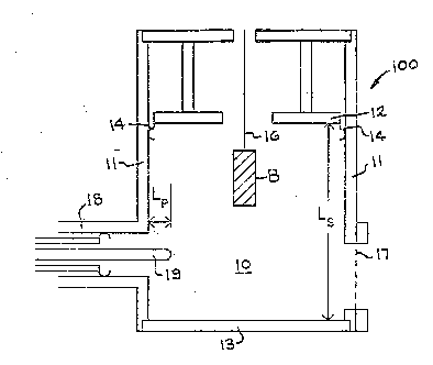
The two prototype cylindrical cavity applicators
are shown in Figure~ 3 and 4. The resonant cavity 10 or
10a is formed by the 17.8 cm inside diameter cylindrical
brass tube 11 or lla and the transverse brass ~horting
plates (or shorts) 12 and 13 or 12a and 13a. One of the
plates 12 or 12a is adju~table to provide a variable
cavity length of 6 to 16cm. The other shorting plate 13 or
13a is fixed in position during operation and is either
soldered to the brass tube 11 as shown in Figure 3 or is
removable from tube lla as shown in Figure 4. Silver
plated finger stock 13b, 14 or 14a provided the required
good electrical contact on the adjustable short 12 or 12a
and the removable short 13a of Figure 4. Four threaded
bolts 15a (two shown) hold the fixed short (13a) in place
on the tube lla d~uring cavity 10 or lOa excitation.
Cavity length variation allow~ the lndividual
selection and matching of diferent cavity modes. ~xample~
of empty cavity modes are TR~ll, TM012~ TE211, TEOll and
TMlll (degenerate mode~), and T~311. Once the cavlty i~
loaded with a material B or Bal then the~e mode~ are
--11 ~
modified (JO Asmus~en~ R. Mallavarpu~ JO ~. Hamann; and H.
C. Park, Proc. IEE~, 6~, 109 (1974)) and become, in
general, hybrid mode~ (R~ F. Harrington, Time-harmonic
Electromagnetic Field~, (McGraw-Hill, New York, 1961) and,
depending on the material B or Ba propertie~ and placement,
new cavity mode~ may be introduced.
The process material B or Ba i9 either su~pended
in the center of the cavity by a cotton thread 16 a~ ~hown
in Figure 3 or rests on the cavi~y fixed ~hort or plate 13a
as shown in Figure 4, or can be placed on a thin teflon
support (not shown). The material can be viewed through a
copper screened window 17. Input microwave power i~ fed
into the coaxial input port 18 or 18a and is coupled into
the cavity via the adjus~able coaxial probe 19 or l9a.
~djustment of plate 12 or 12a length, ~, and coupling
probe 19 and l9a position, Lp, are made by manual or
automatic movement of the probe 19 or 19a or plate 12 or
12a. Short 12 or 12a and probe 19 or l9a positions were
measured to within O.lmm by the micrometer indicators (not
shown).
A rectangular brass piece 20 was soldered onto
the outside of the cylindrical tube 11 parallel to the axi~
of the cavity as shown in Figures 3~ and 4~. Several 12mm,
diagnostic holes 21 or 21a were drilled through this piece
and the cavity wall of the tube 11 or lla at known axial
locations and small electrical E field probes 22 or 22a
made from 2mm o.d. microcoax were inserted into the
diagnostic holes 21 or 21a. When calibrated, these probes
22 or 22a measured the excited cavity radial electric field
strength, ¦Er¦r near the cylindrical wall of the tube 11 or
lla.
I EXPERIMEN'rAL SYSTEM
The experimental heating and processing
measurement~ were performed with a variable power, CW,
microwave sy~t~m. A circuit diagram of thi~ sy~tem i~
shown in Figure 5. It con~i~ts of a (1) ~.45 GHz, CW
varLable power 80urce 99~ t2) clrculator 101 and matched
-12-
dummy load 102, (3~ coaxial directional coupler3 103 and
104, attenuator3 lOS, 106 and power meter~ 108 and 109 that
mea~ure incident power Pi and reflected power Pr~ ~4) a
coaxial input coupling ~y~tem 111 and (5) the microwave
S applicator 112 and material load ~b.
The microwave power coupled into the applicator-
112 is then given by Pt = Pi - Pr. Two different microwave
power sources 99 were employed in ~he experiment~ reported
here~ A sweep generator operated CW at 2.45 GHz was
connected to an amplifier such as a traveling wave tube
(TWT) and provided 0-15W of variable incident power.
~xperiments with higher input powers used a variable power,
15-lOOW, magnetron supply. If on-line material diagnostic
measurements were desired then input frequency was held
constant to less than 0.1 ~Hz during heating. Otherwise,
conventional microwave power sources were used.
Figure 6 shows the equivalent circuit. The
power delivered to the applicator, Pt, divides itself
between the power delivered to the conducting cavity walls
of tube 11 or lla of applicator 100 or lOOa, and the power
delivered to the material load B, Ba or Bb; i.e. Pt = Pb +
Pa when Pb is the power delivered to the applicator walls
and Pa is the power delivered to the material load. A~
shown in Figure 6 and di~cussed in more detail hereinafter
these two quantities can be related to the cavity 10 or 10
fields, the intrinsic resistance, R, of the inside walls of
the tube 11 or lla forming the cavity 10 or lOa, material,
volume VL and the complex dielectric constant of the
material B, Ba or Bb load. The exact division oE the power
between the walls of the tube 11 or lla and the material
load ~, Ba or Bb depend~ on the relative lossyness of the
material B, Ba or~ Bb v~ the lossyness of the cavity walls
of the tub~ 11 or lla.
~190 shown in Yigures 3~, 4A and 5 is a coaxial
E field probe 22 or 22a i~ inserted into the cavity 10 or
lOa and i~ connected through an attenuator 107 to a power
meter 110. Thi~ probe 22 or 22a measure~ the ~quare of the
-13~
normal component of electrlc ield on the conducting
~urface of ~he ~ube 11 or lla. A fiber optic temperature
mea~uring probe 114 is inserted into the cavity 10 or lOa
and i~ mounted on or in the material B, ~a or ~b for
tempera~ure mea~urement.
COUPLING, MF~TCHING AND CONTROL WITEI SIN(;LE MOD~: C~VITY
APPLICATORS
~ n important feature of the cylindrical cavity
applicator~ 100 or lOOa i~ their ability to focu~ and match
the incident microwave energy into the process material B,
Ba or Bb. Thi~ is accomplished with single mode excitation
and "internal cavity" matching. By proper choice and
excitation of a single electromagnetic ~ode in the cavity
10 or lOa, microwave energy can be controlled and ~ocused
into the process material B, ~a or Bb. The matching is
labeled "internal cavity" ~ince all tuning adjustments take
place inside the cavity 10 or lOa. This method of
electromagnetic energy coupling and matching is similar to
that employed in recently developed microwave ion sources
(J. Asmussen and ~. Root, ~ppl. Phys. Letter~, 44, 396
(1984); J. Asmussen and J~ ~oot, U.S. Patent No.4,507,588,
Mar. 26 (1985); J. ~smussen and D. ~einhard, U.S. Patent
No. 4,585,688, April 29 (1986); J. ~oot and J.Asmu~sen,
Rev. of Sci. Instrwm. 56, 1511 91985); ~. Dahimene and J.
Asmussen, J. Vac Sci. Technol. B4, 126 (1986)o The
difference~ with this application are associated with the
controlled, variable coupling to a solid material B, Ba or
Bb in the cavity 10 or lOa.
The input impedance of a microwave cavity 10 or
lOa i~ given by
Pt ~ j2 (Wm~~e)
Zin~ 1 ¦Iol =Rin+iXin (4)
where Pt i~ the total power coupled into the cavity 10 or
lOa (which include~ los~e~ in the metal walls of the tube
11 or lla and plates 12, 12a, 13 and 13a as well as the
power delivered to the material B, Ba or ~b). Wm and We
are, respectively, the time-averaged magnetic and electric
. . .
:~2~ 3
energy ~tored in the ca~ity 10 or 10a fleld~ and /lo/ 1g
the total input curren~ on the coupling probe 19 or l9a.
Rin and jxin are the cavity 10 or 10a input re~istance and
reactance and repre~ent the complex load impedance a3 ~een
by the feed transmission line 111 which i~ the input
coupling ~ystem.
~ t least two independent adjustment3 are
required to match thi~ material a~ Ba or Bb load to
transmission line 111. One adjustment mu~t cancel the load
reactance while the other must adjust the load resistance
to be equal to the characteristic impedance of the feed
transmission system. In the cavity applicator 10 or 10a,
referring again to Figure~ 3 and 4, the continuously
variable probe lg or l9a and cavity end plate 12 or 12a
tuning provide these two required variation~, and together
with single mode excitation are able to cancel the material
B, Ba or Bb loaded cavity reactance and adjust the material
B, ~a or ~b loaded cavity 10 or 10a input resistance to be
equal to the characteri~tic impedance of the feed
transmission line 111 which is the input coupling system.
Internal cavity 10 or 10a matching can best be
understood with the aid of the equivalent circuit shown in
Figure 6. This figure display~ a ~tandard circuit
representation for a cavity 10 or 10a which i5 connected
to a feed waveguide or transmis~ion line 111 and is excited
in the vicinity of a single mode resonance (S. ~amo, J. ~.
Whinnery and T. VanDuzer, Field~ and Waves in Communication
Electronic~ (Wiley, New York, 1967), pp. 565). Gc, Lc and
Cc represent-the conductance, inductance and capacitance,
re~pectively, of the excited mode near re~onance and the jX
repre~ents the reactive effect of the evane~cent mode~ far
from resonance. ~The relation~hip~ between the cavity 10 or
10a fields and the~e equivalent lumped circuit elements is
al~o ~hown in Pigure 6. In an empty cavity 10 or 10a
~ - 1 and VL and ~r 3 throughout the interior
cavlty 18 or 10a volume. Thus, integration~ for Cc and Lc
are over the entire ~avity 10 or 10a volume V. At
~2~3~"'3.~3
--15--
resonance, the capacitive and inductive ~uscep~ance cancel
resulting in a purely conductive input impedance. In
Figure 6, the coupling probe 19 or lsa i8 represented a~ a
l~mped reactance jX and the ideal transformer of turn~
ratio m:l. aoth circuit element~ and ~he tran~former m:l
are drawn with arrow~ to indicate thelr variabllity during
the tuning proces~.
When the material B, Ba or Bb load i~ placed in
the empty cavity 10 or lOa each electromagnetic resonance
is shifted down in frequency and Q i8 lowered~ The
pre3ence of the material ~, Ba or Bb load then changes Lc,
Gc and Cc and adds an additional material B, ~a or Bb
conductance GL and susceptance, jBL, to the circuit. ~s i~
shown in the equations in Figure 6 theqe additional circuit
elements are functions of the material B, Ba or 8b load
placement, volume, shape, and material B, Ba or Bb
properties. The electromagnetic resonance shift is then a
function of these properties.
The material B, Ba or Bb load is irradiated
with microwave energy by ~ir~t adjusting the probe 19 or
l9a and cavity 10 or lOa leng~h positions with plate 12 or
12a to excite a specific loaded cavity 10 or lOa resonance
and to match the cavity 10 or lOa applicator to the input
transmission system. The specific electromagnetic mode
chosen depends on the ~hape and location of the material B,
8a or Bb load. For example, if ~he material B, Ba or Bb is
cylindrical and located in the center of the cavity as
shown in Figure 7 in per~pective view then the loaded
cavity 10 or lOa TM012 mode with it~ high electric field
along the cavity 10 or lOa axi~ is a logical proce~sing
mode as also ~hown in Figure 3. If the material B, Ba or
Bb is a thin ~la~ located in the bottom of the cavity 10 or
lOa as shown in Figure 4 then either a T~ mode or TM mode
appear to be good choice~.
Once adjusted for ~ match in the pre~pecif iea
mode, microwave power 1~ then applied, absorbed into the
cavity 10 or lOa without reElection, and heating o the
.
..... _ . . .. . . . . . . ... .. . . . . ... .
-16-
material B, Ba or Bb then begin~. This heating then
changes the material B, ~a or Bb propertie~. In
particular, Ewill ta~e on new values re~ulting in a ~hift
in the cavity 10 or lOa re~onance ana a change in
applicator tube ll or lla input impedance. Thu~, during
processing the applicator 100 or lOOa length by means of
plate 12 or 12a, L~, and coupling probe 19 or l9a
penetration, Lp, are varied iteratively until reflected
power is reduced to zerc, i.e., during processing the
applicator is matched as material B, Ba or Bb properties
change. Typical tuning distances are on the order of
several millimeter~ requiring precise measurement. The
tuning process can be quickly performed either ~anually or
with small motors (not shown) attached to the probe 19 or
19a and plate 12 or 12a. This tuning can also be utilized
as a simple input power control technique.
The ability to be mechanica].ly tuned serve~
other practical functions. In addition to mode selection
and matching it allows difEerent material e, Ba or ~b loads
to be matched to a given constant frequency power source.
Variations in cavity 10 or lOa resonant frequency caused by
(1) cavity 10 or lOa expansion or contraction due to
ambient temperature change~ ~C. G. Montgomery, Technique
of Microwave ~easurements, Vol. 1, (~over Pub., New York,
N.Y. 1966), pp. 384) and (2) relative humidity changes in
the air (C. G. Montgomery, Technique Oe Microwave
Measurement~, Vol. 1, (Dover Pub., New York, N.Y. 1966),
pp. 384) inside the cavity 10 or lOa can al30 be cancelled.
Fre~uency drift~ caused by variations in output power and
heating of the power oscillator 99 can be compensated for
by mechanical tuning. Finally, it allows the applicators
100 or lOOa to b~ used with power oscillator~ 99 which
oscillate at different frequencies.
BASIC EQUATIONS AND MEASUREMENTS TECHNIQUES
In the experiment~ reported here, ~everal
material B, Ba or Bb sample~ were excited and heated with
electromagnetic energy~ The material volumes were
. . .
.. . . . . . . ~ .. . . . . .. . ... . . . . . . .
-17-
intentionally kept small, and ~imple shapes, such a~ di~ks
and cylinders, were cho~en in order to be able to combine
experiments with electromagnetic perturbation theory tR. F.
Harrington, Time Harmonic Electromagnetic Fields,
(McGraw-Hill, New York, 1961); C. G. Montgomery, Technique
of Microwave Measurements, Vol.l, (Dover Pub., New York,
N.Y., pp. 384 (1966)). Larger material volumes require a
more exact, complete electromagnetic analysi~ of the
material loaded cavity.
A number oE meaqurements were perormed
to evaluate the cavity applicator per~ormance. Among these
were the measurement of material complex dielectric
constant, material loaded cavity quality factor, and
applicator coupling efficiency during electromagnetic
heating. The techniques of measurement of each o~ these
quantities are described below.
The principal mode used to demonstrate the
heating and simultaneous diagnosis was the TM012 mode which
is shown in Figure 7, exciting a small cylindrical sample.
Using conventional perturbation theory for such a material
loaded cavity 10 or lOa it can be shown that ~R. F.
Harrington, Time-harmonic Electromagnetic Fields,
(McGraw-Hill, ~ew York, ~1961))
~ )o~ (1 - E~ ZO ~ ~
J ( 5 )
and 1 1 ~ E ~ VL ~ I ~
Qu QO r ~ J ¦EO ¦ dv 7 (6)
.
. . . . . . ... . . . .. , . . . . . _ .. .. . ... . .
-la-
where
- empty cavity resonant Erequency
materlal loadea cavity resonant fr~quency
and cavity proces~ing freqllency
QO= emp~y cavity quality factor
Qu= material loaded cavity quality factor
- Eo ~ r) ~ the real and imaginary
parts of the material complex dielectric
constant~
Ezo= empty cavity TM012 mode axially directed
electric field
= magnitude of the empty cavity electric
field strength
VL- material volume
V= empty cavity volume
The empty cavity 10 or lOa electric field strengths are
well known for the T~012 mode and thu~, for a given
material B, Ba or Bb sample with radiu~ r, and length 1,
the integral~ of equations ~S) and (6) can be determined.
Thus~ if Qu~ Qo~ ~and ~O are measured, then ~r and ~'r can
be calculated from equation~ (5) and (6)~
Conventional complex dielectric constant
measurement technique~ u~ually employ a low power, swept
frequency signal to measure quality factor and re~onant
~requency with and without a material B, Ba or Bb load (C.
G. Montgomery, Techniyue of ~icrowave Me~surements, Vol. 1,
(Dover Pub., New York, N.Y. pp. 384 (1966); and S. Li, C.
~kyel and R. G. Bosisio, IEEE Trans. Microwave Theory,
MTT-29, 1041 (1981)). If the material B, ~a or Bb i~
simultaneou ly being heated or proce~sed with microwave
energy, which ha~ a field inten~ity o~ one hundred to one
thou~and time~ that of the low power diagnostic ~ignal,
then the leakage o the high power heating energy into the
diagno~tic circuits often impair mea~urements. Here, a
different technique i~ employed. The h~gh input power
exciting field~ of the TMol~ mode are u~ed to both heat and
diagnose~the material as proce~sing occurs.
.
.
, . ... . . , . . . . .. . ., .. , . . .... , .. .. . .. ... ~ . .. .. .. . . . ... . .. . . . . ..
-lg ~
The measurement technique employed ha~ been
de~cribed in detail earlier ~J~ ~ogers, Ph.D. Thesls, 1982,
Michigan State University) and, thus, is only summarized
briefly here. An important a~sumption of the measurement
5 i3 that the presence oE the material ~, Ba or Bb load doe~
not significantly alter the spatial distribution of the
cavity wall currents from those of the empty cavity 10 or
lOa TM012 mode. Evidence supporting this a~umption i~
that only very small experimental changes in resonant
length are required to match the material cavity lOa or lOb
from empty cavity 10 or lOa to material loaded operation,
i e., the material B, Ba or Bb loaded operation is a small
length perturbation from empty cavity lOa or lOb resonance.
Experimental measurements of the axial distribution of Er
at the cavity lOa or lOb walls with microcoax probes showed
the presence of a spatially sim;lar, T~012 standing wave
adjacent to the cavity lOa or lOb walls both with and
without different material s, Ba or Bb loads. Finally, the
exact numerical solutions for the cavity lOa or lOb ~ield
distributions with the 105sy material present differ from
the empty cavity lOa or lOb distributions only near the
material B, Ba or Bb in the cen~er of the cavity lOa or lOb
tJ. Rogers; Ph.D. Thesis, 1982, Michigan State University),
i.e., the cavity lOa or lOb wall current distributions for
the TM012 mode change very little with the presence of the
material B, ~a, or Bb.
Under the above mentioned conditions, the ratio
of the radial electeic field measured at a fixed position
on the cavity lOa or lOb wall to the total power absorbed
by the walls is a constan~ with and without a material
B, Ba or Bb load, i.e.,
eb
~ 2 - con~tant
Before heating and processing9 complex
dlelectric constant of the cylindrical materLal B, Ba or Bb
load was measured at room temperature using conventional
3~3
-20
low power swept frequency measurements of applicator
100 or lOOa quality factor and re~onant freq~ency with and
without the material B, Ba or Bb load~ The initial room
temperature complex dielectric con~tant wa~ then determined
s from equations t5) and ~6).
Initial measurement~ also included the CW
excitation of the empty cavity lOa or lOb at the proces~ing
frequency with a low power tP~t signal Pto and the
simultaneous mea~urement of ~he radial electric field /Ero/
when the cavity lOa or lOb was critically coupled.
During this measurement, the applicator 100 or lOOa was
critically couplea at ~ by adjusting Lp and Ls. ~fter
recording thi~ measurement, the material B, aa or 8b load
was placed exactly in the center of the applicato~ 100 or
lOOa and then Ep and Ls were readjusted for critical
coupling at ~. Input power was then raised to the desired
level and material B, Ba or Bb heating began. ~s the
~aterial B, Ba or ~b load was heated, its properties
changed which in turn detuned the cavity lOa or lOb. The
applicator 100 or lOOa was continuously tuned for zero
reflected power during the heating cycle.
During heating, data points of cavity 10 or lOa
length, probe 19 or l9a position, total power absorbed by
the cavity, Pt, cavity field strength, /Er¦2, were recorded
at prespecified time intervals. Loaded cavity 10 or lOa
quality factor was determined for each data point from the
following equation
QoPto / ~ ~8)
Qu= /Er/Z Pt
and cavity 10 or lOa wall lo~se~ were determined fro~
/Er/2
Pb=/Ero/2 Pto ~9)
Note, since both equation~ (8) and ~9) require the ratios
of the electric fields, only mea~urement~ of the relative
magnitude~ of eLectric field were necessary.
.. . _ . _ _ . _ .... . .. . .. . . .. . .. _ .. .. .. . . . . . . .. . ... . ., . .. _ _ _ _ _ _ .. . ..
.... . . . _ .
33
-21-
After completing a heating cycle, tha material
B, Ba or ~b wa~ removed from the cavity 10 or lOa and the
empty cavity lO or lOa wa~ returned to e~ch ~eparate data
point position for Lg and ~. The empty cavity 10 or lOa
rPsonance frequency wb was then measured for each
experimental data point. Then u~ing equations t5) and (6) f
the complex dielectric con~tant was determined~ For very
accurate calculations of E empty cavity 10 or lOa
measurement~ ~hould be made under the same temperature and
relative humidity condition~ that were pre~ent during
processing.
It is also useful to determine the ef~iciency of
coupling microwave energy into a load ~aterial B, Ba or ~b.
Thus, a system ~figure of merit~, called the overall
coupling e~ficiency of the material loaded applicator 100
or lOOa, is defined a~
~Eff)l = lOOx Pi (10)
where æi = Pr + Pt = Pr + Pa + Pb. Viewing the applicator
100 or lOOa a~ an impedance transformer and a focusing
device, the ideal applicator 100 or lOOa will deliver all
the incident power into the material B, Ba or Bb with zero
reflected power and applicator 100 or lOOa wall 105~ power;
i.e., Pi = Pt = Pa~ Pr and Pb = and the overall coupling
efficiency will then be 100%. In all experiments reported
here the reflected power can be reduced to a very small
value by tuning adjustments, i.e., Pr Pi. Then the
overall coupling efficiency i~ equal to just the applicator
coupling efficiency (Eff)2 i.e.,
tEff)2-100 ~x Pt = 100 x Pa + Pb 3 100 [1 - QO] (ll)
EXPERIMENTAL RESVLTS
The experimental perormance for ~everal,
~imple, well unaer~tood makerial~ B, Ba or Bb is presented
below and demonstrates applicator 100 or lOOa operation
. .. . :. _, , . . . .. .. .. .. ....... . . _.. ... . .. . . .
~. ~9~
-22-
with a wide range o~ material load~. The3e material~ are
nylon, wet wood, water cylinder~, and a three inch 3ilicon
wafer. Nylon i~ a relatively lo~syless material, wet wood
is moderately lossy~ water i~ very lossy with a high
dielectric constant (~80), and the ~ilicon wafer
demonstrate~ operation with a thin ~emiconducting material.
The applicators lOOa were experimentally
demonstrated u~ing the experimental set up of Figure S.
Cylindrical material rods were heated by placing them in
the center of the applicator 100 of Figure 3 and by
exciting the cavity with the T~012 mode as shown in Figure
7. Material slabs or thin disks were placed at the end oE
the cavity applicator lOOa as shown in Figure 4 and were
excited with either the TM or TF, modes. These materials
lS loads were either placed directly on the applicator fixed
short 13 or 13a or were'placed on thin teflon supports (not
shown). The experimentally measured v~riations of material
temperature, coupling efficiency and, when,possible,
complex dielectric constant are summarized below for each
material load.
( NYLON ~
Nylon 66 cyl~nders af length 3.1 cm and radius
0.65 cm were heated and diagnosed with the same exciting
TM012 electromagnetic fields. ~ fiber optic temperature
probe was placed parallel to the cotton thread and was
inserted axially through a small tightly fitting hole into
the center of the nylon cylinder. Thus, the internal
temperature of the nylon was measured a~ the microwave
energy was applied.
The nylon cylinaer was placed exactly in the
center of the applicator 100 and the room temperature
complex dielectr~c con~tant was measured with very low
microwave power levels u~ing standard cavity perturbation
techniques. The room temperature dielectric con~tant
agreed with published data (S. Li~ C. Akyel and R. G.
Bosi~io, IEEE Trans. Microwave Theory, MTT-29, 1041 ~1981)).
Then microwave power wa3 increa~ed and the applicator wa~
.
.~2~3r~3
-23-
continuously tuned to a match. The measurement technique
outlined in the previou~ section was used to evaluate
applicator performance and material propertie~. ~hat i~,
during heating, data points of cavity leng~h and probe 19
positions, incident power, cavity /Er/2 field ~trength and
nylon t~mperature were recorded at one minute intervals.
Lp and L~ positions were measured to within one-tenth of a
~illime~er and frequency was measured to withi~ a tenth of
a MHz.
Figure~ 8A and 8B display the measured nylon
complex dielectric con~tant vs. time and Figures 9A and 9~
display the same data plotted v~. the measured temperature.
The results ~or two ~ypical heating cycles of 3 w and 5 w
applied to two different nylon cylinders are displayed in
each Figure. ~s shown, nylon changes from a relatively low
loss to a very lossy dielectric as heating progresses. In
fact, the shape of the ~r curves indicates the potential
for thermal runaway (H. F. Huang, J. Microwave Power, ll,
305 tl976); and G. Roussy, A. Mercier, J. Thiebunt and J.
Vaubourg, J. Microwave Power, 47 (1985)). Data for nylon
66 available from the literature (H. F. Huang, J. Microwave
Power, 11, 305 (1976)) is al~o di~played in Figure 10 and
show good agreement, i.e. within several percent with
measured data below the softening temperature (-65C) of
nylon 66. ~t higher temperature~ the accuracy of the
measured data decreases presumably due to the nylon rod
thermal expansion and deformation, and changes in the
cavity wall temperature and cavity air temperaturer and
humidity. Coupling efficiency calculated using equation
(9) begin at 40~ at room temperature and time t=0, and
gradually increase to 85-95~ at the end of the heating
cycle.
Figure~ 8A, 8B, 9A and 9B clearly demon~trate
that changes in input power of only a few watts
dramatically alter~ the heating cycle. The dielectric
constant follows a different "path" vs. time for different
input powers. In fact, experiments with larger input
" ,, . .. , ,, . ~, . _ .. ... ... . .. . . . .
-2~-
power~ of >10W ~data point3 not ~hown) lPad to the
explo~ive de~truction oE the nylon roa due to non-uniform
overheating due to thermal runaway in the center of the
nylon. On-line mea~uremen~ of the nylon comple~ dielectric
constant provides knowledge of material heating and
material propertie~ (note ~he relation~hip between
temperature and ~r of Figures 9~ and 9B, and thu3 can be
used as a feedback signal or process control. Using the~e
on-line measurements the heating cycle i~ adju~ted to
prevent material destruction and ~o yield processed
materials with the desired properties.
WET WOOD
The drying of paper and wet wood is an old use
of microwave energy. Here the single mode applicator 100
is demonstrated by dryinq water soaked wood rods. The
results of drying experiments, which were similar to the
above described nylon heating experiments, are displayed in
Figures 10 to 12. Complex dielectric constant of the wood
material B wa~ measured vs time Eor 5W and aw drying
cycles. ~lso displayea is the coupling efficiency vs. time
as the water is driven from the wood. Note that initially
the overall coupling efficiency i~ high ~~90%) and
decreases (to 70%) as drying progresses. Its variation
with ~ime depends on the actual heating cycle chosen.
These experiment~ clearly show that as the wood is dried,
the division of the constant input power Pt, varies between
the wet wood and the cavity walls; i.e., as the wood load
becomes drier, and hence less lossy, more power is supplied
to the cavity wall~. As drying take~ place the wet wood
complex dielectric constant converges to the dry ~ .
The initial weight WO~ and final weight Wf, of
the wood rod~ an~ the total energy supplied to the
applicator during the heating time were recorded in e~ch
experimental run. Thu~, the drying efficiency, i.e., the
ratio of the total energy input into the applicator to the
total energy requirea to evaporate water of weight W -
Wo-Wf, was calculated, a~ indicated in Figure 12, for
3~
-25-
two different twelve minu~e drying cycle~. Over thi~
period the drying efficiency of the 5 W run i3 60% while
that o the 8 W run is 50%. The experimental data for
Er indicate~ that when 8W i~ applied the wood i~ dry
after nine minutes. IE the drying cycle for 8 W i~ then
stopped a~ 9 minute~ the drying efficiency improve~ to 66%.
It i~ clear that on-line measurement of E during the actual
drying proces~ can be u~ed a~ a method of proces~
monitoring and provide~ informa~ion for process control and
optimization.
W~TER CYLINDERS
Cylindrical, one mm thick, quartz tube~ with an
inside diameter of 0.205 cm and a length of 4.2 cm were
filled with distilled water and were hung from a cotton
thread in the center of the applicator 100 a~ shown in
Figure 3. Using ~everal constant input power levels of 1~,
1.5W, 2W etc, the manually matched watet samples were
heated to a boil by excitation with the T~012 mode.
~xperimental measurements similar to those de~cribed for
nylon and wood were taken as the water temperature wa~
increased from room temperature to boiling.
A~ is well known, it i~ not pos~ible to
accurately measure ~ ~or the large volumes of water used in
these experiment~ by using cavity perturbation theory (S.
Li, C. ~kyel and ~. G. Bosisio, IEEE Trans. Microwave
Theory, MTT-29, 1041 ~1981))o However, measurements were
repeatable and provided information on the state of water
heating. Typical result~ for several experimental runs for
~ vs. temperature are shown and compared with published
data ~A. R. Von ~ippel, Dielectric Material~ and
Applications (MIT Press~ Cambridge, MA. 1954), pp. 361) in
Figure 13.
Overall microwave coupling efficiency varied
from 91~ at the beginning of the heating to 82~ at boiling,
5 minutes later. These result~ are very good for ~uch
small water ~ample~. Larger ~ample~ will yield higher
.
.. . __ . _ . . . . . .. _ . . _ . , . ... .. .. . _ . , .... , . . .. .. .. ., _ _ . . . ... .. ..
. .. _ . .
~26-
coupling eff;ciencie~ ~ince loaded Q i~ proportional to
material volume.
S~MICONDUCTOR WAF~RS
Earlier experiment~ concerned with oxidation of
~ilicon in a microwave plasma dis~ reactor ~T. Roppel, D.
. Reinhard and J. Asmu~sen, J. Vac. Sci. Technol. B~, 195
(1986)) nsted that in the ab~ence of a mic~owave discharge
a ~mall ~ilicon wafer could be quickly heated with
microwave energy to cherry red (~900C) in a ~ingle mode
cavity applicator (T. Roppel, PhD Thesi~ L9~6, Michigan
State University). Investigating thi~ phenomenon further a
three inch wafer Ba was placed in atmospheric air on a 3 mm
thick ring of teflon placed on the end plate 13a of the
cavity 10a applicator 100a shown in Figure 4. The
applicat~r 100a was excited and continuously manually
matched in the TElll mode. Figure 14 displays the
temperature vs. time for thi~ waer Ba excited with l9.5W
and 37W of input power. The initial rate of change of
wafer Ba temperature was 94C/min for l9.5W input and
172C/min for 37W and i~ thus proportional to the power
absorbed in the cavity 10a. The wafer 13a temperature
quickly reached 240C ~the maximum of the Eiber optic 114
measurement system) with only 37 W of input power. Much
higher steady state temperature are possible with higher
input powers. At room temperature the ~kin depth for the
electromagnetic Eield in silicon i~ ~2.6 mm and thus good
electromagnetic field penetration into the 0.4 mm thick
wafer is pos~ible. The~e experiments clearly demonstrate
that these applicator~ 100a can couple to thin
~emiconducting materials Ba, increasing the material Ba
temperature~ to very high value~. Thu~ the~e applicators
can be u-~ed ag plroces3ing controlled high temperature,
efficient, electric furnace~.
CONCLUSIONS
When considering de~ign criteria, such a~ high
coupling efficiency, proce~s controlability and heating
uniformity, the single mode (or controlled multimode)
. _ _ _ _ . . .: .,., .. _ _ ._ ., . . .. .. . . , _ ., .. .. _ _. _ _ __ . _ . . .. . . . .... . _ . .
_ ,
27
cavity applica~or ha~ importan~ advantages over
conventional multimode appllcators. For example, heating
uniformity and control ~an be achieved by placing material
B, Ba or Bb represen~ing ths load in the proper position in
the single mode exciting field4. Thi~ placement of the
load in an elec~romagnetic focused zone in~ide the
applicator 100 or 100a al~o improves the coupling
efficiency of the applicator 100 or 100a. Since applicator
100 or 100a wall~ can be made of highly conductive material
(and can even be cooled to very low temperature~), the
unloaded cavity applicator 100 or 100a can be designed as a
high Q device and thus a high percentage of the input
ener~y is transferred to the load. By using internal
cavity 10 or 10a matching and single mode excitation the
applicator 100 or 100a can be matched to the feed
transmission line 111 throughout the processing cycle and
all the incident power is coupled into the applicator 100
or 100a and i~ distributed between the material B, Ba or Bb
load ana the conducting appLicator 100 or 100a wallsO
The experiment~ described demonstrated that
single mode cavity 10 or 10a applicators 100 or 100a can
efficiently couple microwave energy in~o a wide range of
material B, Ba or Bb loads. ~aterial B, Ba or Bb loads
ranging Çrom low los~y, such a~ nylon, to very lossy, such
as water, and semiconducting materials, such as silicon
wafers, were efficiently heated. Overall coupling
efficiencies of 7~-95% were measured, using bras~
applicators 100 or 100aO
The use of single mode excitation ha~ the
benefit of allowing on-line diagno~i~ of material
B, Ba or B~ propertie3 during proces3ing. Processing of
epoxies, graphitqs and other compo~ite material~, thin
conductin~ and ~emiconductlng materials and even biological
material~ can be accompli~hed by the method of the pre~ent
invention. If high accuracy i~ de~ired, microwave power
~ources with good frequency stability (< .1 MHz) are
required, and applicator 100 or 100a and material B, ~a or
... . . . .. .. ..... . ... . . .. .
...... . ... ... . . . . . , _ . . __. __ .. _. , ., , _ .. ,. _, _ _ ., _ . , . _
q~
-28-
Bb size varia~ion~ with temperature mu~t be taken into
account.
esults
The Example~ demonstrate the ability of the
method of the pre~ent inventlon to precisely control the
heating of materials B, Ba or Bb. Many variable~ such as
input power control, tuning control, excitation frequency
controi ~instead of applicator length tuning) are available
as process control variables. In addition, other system
variables such as cavity 10 or lOa electric field strength
(and hence material B, Ba or Bb field strength), cavity
10 or lOa size, etc. are also available as process system
feedback signals for an automated, intelligent processing
system.
~esign concepts employed in cavity lOa or lOb
applicator 100 or lOOa construction can be generalized to
rectangular cavities and can also be scaled with Erequency.
The cavity 10 or lOa applicator 100 or lOOa concepts have
been demonstrated, at 2.45GHz in the Examples. However,
larger material B, Ba or Bb loads can be processed by
simply scaling the applicator 100 or lOOa design to lower
excitation frequencies~ For example, by reducing the
excitation frequency to 915 MHz or to 400 ~Hz, the material
B, Ba or Bb load sizes can be increased by three to five
times.
It is intended that the foregoing description be
only illustrative and that the present invention be limited
only by the hereinafter appended claims.
.. . . . ......................... ... ... .
. .. _, .. .. . . . ... . ., .... . ~, .. . , . .. . .. __ .___ . ___ ., .. _ . .. . . . .
.