Note: Descriptions are shown in the official language in which they were submitted.
f-~06
B~CKGROUND OF THE INVENTION
1 1 Field of the Invention
The present invention pertains to time interval to digital
converters particularly with respect to smoothing the digital
output to eliminate jitter.
2. escription of the Prior Art
It is often desirable in the prior art to convert a time
interval to a digital signal. In practical systems in which such
a conversion may be utilized, time jitter at the boundaries of the
time interval may cause the digital signal to vary erratically
resulting in anomalous behaviour in the system. Such time
intervals are often represented by pulse width modulated signals
where the width of the individual pulses are the time intervals to
be converted.
Such conversion of pulse width modulated signals into digital
format is encountered in airborne radar systems having an antenna
mounted in a radome on the aircraft wherein the antenna scans in a
reciprocating sector scan manner. A resolver coupled to the
antenna shaft provides AC voltages proportional to the sine and
cosine of the azimulh angle of the antenna. These sine and cosine
voltages are transmitted to a display unit in the aircraft via
shielded wiring. In a well-known manner the sine and cosine
signals are converted to a variable width pulse where the pulse
width is related to the antenna azimuth angle. The variable width
pulse is converted to a digital word by known techniques to
address an XY memory utilized to store the radial lines of the
received radar information. Each location in the memory
corresponds to an incremental azimuth angle. In a typical
~ ~?~
--2--
1 system, the sine and cosine voltages may be converted into a 10
bit parallel digital azimuth address word which would provide the
capability of storing 1.024 radial lines of radar data in the
memory. me memory is rapidly read out to drive a CRT display on
which the radar data is written in PPI sector scanning manner.
Errors such as noise, hum and mechanical cogging of the
antenna result in jitter in the digital addressing word. This
jitter disturbs the uniform memory accessing such that radial
lines of memory may randomly not be written to. mis results in
anomalous and undesirable random black radial lines in the CRT
display giving the appearance of uneven motion of the antenna.
Such uneven motion would result in no data being written to memory
from the incremental azimuth angles represented by the lines.
Various techniques have been utilized in the prior art in an
attempt to obviate the anomalies caused by jitter. Analog low
pass filters to process the sine and cosine signals so as to
filter out the jitter signals results in undesirable follow-up
delay. Digital signaling techniques may be utilized to convert
the antenna azimuth angle into digital format at the antenna.
mis requires the addition of a significant amount of circuitry to
be installed in the hostile environment of the radome. A further
technique utilized in the prior art is to slew a counter with a
voltage controlled oscillator, the frequency of which being
determined by azimuth feedback from the antenna. For example,
sine and cosine potentiometers or synchros coupled to the azimuth
axis of the antenna may be utilized to provide these signals.
Such a technique suffers from the disadvantage that directional
reversals of the sector scanning antenna cannot be accurately
~96906
3 7255
followed at the end pOillts Thus, the prior art techniques
cannot provide an accurate digi~al representation of the
position at the end points when the antenna is experiencing a
reversal from full scanning speed in one direction to ful~
scanning speed in the opposite direction.
SUMMARY OF TH~ INVENTION
The disadvantages of the prior art are obviated by
the time interval-to-digi~al converter of the present invention
wherein the antenna azimuth angle is converted to a variable
width pulse and an up/down counter is slewed at a slow rate so
that the count stored therein is a digital representation of
the width of the pulse. A second counter responsive to the
output of the up/down counter is loaded with a count
representative of the up/down counter output. A clock signal
is applied to the second counter to count from the value loaded
therein during the duration of the next variable width pulse
and the final count of the second counter is utilized to
increment or decrement the up/down counter so that the output
thereof accurately tracks the width of the pulse. Hysteresis
may be utilized in this slewing process.
In accordance with the present invention there is
provided a time interval to digital converter for converting an
input signal representative of said time interval to a digital
output signal, comprising digital up/down counter means for
providing the digital output signal, further digital counter
means responsive to the digital output signal and to the input
signal for loading the digital output signal therein and
counting therefrom during the time interval, thereby providing
a digital error signal, and correction means responsive to the
digi~al error signal for controllably incrementing or
decrementing the digital up/down counter means in accordance
with the digital error signal so that the digital error signal
tends toward zero.
~296906
3a 72558-13
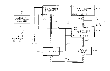
BRIEF DESCRIPTION OF THE DRAWING
The sole figure is a schematic block diayram of a
time interval-to-digital converter implemented in accordance
with the present invention.
DESCRIPTION OF THE PREFERRED EMBODIMENT
The time interval-to-digital converter illustrated in
the figure may be utilized in any application requiring the
conversion of a time interval into a digital representation
thereof. For purposes of discussion, the converter of the
preferred embodiment will be described in terms of providing a
parallel digital representation of the azimuth angle of a
sector scanning
12~i'306
1 antenna. An angle-to-pulse width converter 10 provides a variable
pulse width signal on a line ll where the negative going pulse
width intervals thereof are proportional to the azimuth angle.
'rwO such pulse width intervals are illustrated at 12 and 13 in the
figure. The angle-to-pulse width converter 10 may, for example,
receive voltages proportional to the sine and cosine of the
azimuth angle, for conversion, in a manner well known in the art,
into the pulse width modulated signal on the line 11.
~he pulse width modulated signal on the line 11 is applied to
the load input of an 11 bit down counter 14. The data load port
of the counter 14 is denoted as A10-A0, the ten least significant
bits A9-A0 thereof receiving the parallel output D9-D0 of a 10 bit
up/down counter 15. The count from the counter 15 is applied to
the data load port of the counter 14 via a 10 conductor bus 16
which also provides the 10 bit parallel digital output data in a
manner to be described. The most significant digit A10 of the
data load port of the counter 14 is connected to ground
potential. A clock signal at a terminal 17 is applied to the
clock input of the counter 14 for controlling the downward
counting thereof. Prior to the beginning of a pulse width
interval to be converted, the load signal on the line 11 is in a
high state and the output data from the counter 15 is cvntinuously
loaded to the counter 14. When the pulse width modulated signal
on the line 11 goes low at the leading edge of the time interval
to be converted, the counter 14 is enabled to count downward
toward zero from the count then existing at the data load port
A10-A0 thereof.
The 11 bit output D10-D0 from the counter 14 is applied via a
bus 18 to address an increment/decrement decision PROM 19. The
output of the PROM 19 (Programmable Read Only Memory) is, in the
illustrated embodiment, a 3 bit message that is applied to a 3 bit
latch 20 via a bus 21. When the pulse width modulated signal on
~29t~90~;
l the line 11 goes high at the trailing edge of the pulse width
interval to be converted, the counter 14 is placed in the reload
mode thereof. Simultaneously, the count remaining in the counter
14 at the end of the time inteeval to be converted addresses the
PROM 19 to generate the 3 bit message on the bus 21. This message
is latched into the latch 20 by the rising trailing edge of the
pulse width modulated signal. Thus the message on the bus 21,
which is generated at the end of the time interval to be
converted, is an expression of the count remaining in the counter
14.
It is appreciated that the rising edge of the pulse width
modulated signal on the line 11 controls the counter 14 to
commence reloading output data into its data load port A10-A0
while it is latching the message on the bus 21 into the latch 20.
The correct message will be latched into the latch 20 despite the
apparent race condition that exists upon the occurrence of the
rising edge of the pulse width modulated signal on the line 11
because of the propagation delays of the PROM 19.
me 3 bit message stored in the latch 20 is applied to a bit
pattern generator 22 at the bit pattern conmand (BPC) input
thereof via a bus 23. The bit pattern command on the bus 23
commands the bit pattern generator 22 to generate controlled
bursts of pulses and to apply these pulses selectively to the up
input or the down input of the counter 15. Thus the output data
signal on the bus 16 is maintained as equal as possible to the
current width of the pulse width modulated signal on the line 11
in terms of periods of the clock signal applied to the terminal
17. me counter 15, therefore, develops the output data on the
bus 16 by being incremented or decremented by the bursts of pulses
fron the bit pattern generator 22 in a manner to be further
explained.
lZ'3fi9~i
- 6 - 72558-13
The bit pattern generator 22 also receives the pulse
width modulated signal on the line 11 at the sync input thereof
as well as the clock signal at the terminal 17 at the clock
input thereof. When the pulse width modulated signal on the
line 11 is low (during an interval 12 or 13), the bit pattern
generator 22 is maintained in a reset state during which no
pulses are applied to the counter 15. When the pulse width
modulated signal on the line 11 goes high, the pulse bursts are
applied controllably to the up or down input of the counter 15
so that the count in the counter 15 tracks the width of the
pulses on the line 11. The bit pattern generator 22 may be
configured to provide pulse bursts in accordance with the
following Table 1:
TABLE 1
ERROR REMAINING MESSAGE CORRECTION TO
IN COUNTER 14 (BPC) COUNTER 15
11 or more 1 1 0 8 decrements
2 to 10 0 1 0 2 decrements
1 1 0 0 1 decrement
0 0 0 0 No change
-1 0 1 1 1 increment
-2 to -10 1 0 1 2 increments
-11 or more 0 0 1 8 incre,ments
In accordance with Table 1 if the error remaining in
the counter 14 at the end of a pulse width interval to be
converted is 11 or more counts, the PROM 19 converts this count
into the bit pattern command message delineated in Table 1
which controls the bit pattern generator 22 to apply 8 pulses
(16
- 7 - 72558-13
to the down input of the counter 15. The bit pattern generator
22 is enabled to provide these pulses when the sync signal goes
high. In a similar manner if the error remaining in the coun-
ter 14 is -11 or more the bit pattern generator 22 applies 8
pulses to the up input of the counter 15. It is appreciated
from Table 1 that if the value in the counter 15 exactly mat-
ches the width of the pulse width modulated signal on the line
11, the counter 14 will be at zero at the end of the pulse
interval. The PROM 19 will provide a message interpreted in
the bit pattern generator 22 as "No change" and the counter 15
will be neither incremented nor decremented. If however the
counter 14 is not at zero at the end of the pulse width inter-
val to be converted, the value remaining in the counter 14
represents the error between the value in the counter 15 and
the width of the pulse interval to be converted resulting in
the PROM 19 generating a message providing the controlled in-
crement or decrement of the counter 15 in accordance with Table
1.
The top and bottom lines of Table 1 represent a slew
mode for the device. If the residual errors are above a pre-
determined threshold (in Table 1 the threshold is 11), the
device is operated in a high-speed slew mode that will provide
rapid alignment. It is appreciated from Table 1 that when the
error is 11 or more, bursts of 8 pulses are utilized to rapidly
align the counter 15 with the width of the pulses. This provi-
sion is primarily utilized at start-up. The pulses provided by
the bit pattern generator 22 to the counter 15 are in synchron-
ism with the clock signal applied to the clock input thereof.
It is appreciated that in any conventional
12~ 6
--8--
-f h~ o i l .f~
1 circuit to provide the f~mction delineated in Table 1 may be
utilized. The design of circuits for controllably applying pulse
bursts to the up and down inputs of the counter 15 as described in
Table 1 is well within the skill of the routineer in the art.
It is appreciated from the foregoing that the apparatus of the
figure comprises a digital servo wherein the error signal in the
counter 14 results in adjustments to the counter 15 via the bit
pattern generator 22 that slave the digital value in the counter
15 to the width of the pulses applied to the line 11. The upward
and downward adjustments of the counter 15 are such as to tend to
drive the error signal in the counter 14 to zero.
It will be appreciated that errors of 2 to 10 counts all
result in 2 increments or decrements to counter 15. Since, in
this implementation, the system averages 1.6 counts for each cycle
of the pulse width modulated signal 11, the counter 15 can readily
follow variations in the input. Since black radial lines are only
visible if jumps of more than 4 counts occur, this invention
prevents their occurrence by preventing jumps of more than 2
counts.
Hysteresis may be added to the system by simply utilizing
additional "No change" messages as follows:
TaBLE 2
ERROR REMAINING MESSAGE CORRECTION TO
IN COUNTER 14 (BPC) COUNTER 15
11 or more 1 1 0 8 decrements
3 to 10 0 1 0 2 decrements
2 1 0 0 1 decrement
1 0 0 0 No change
0 0 0 0 No change
-1 0 0 0 No change
-2 0 1 1 1 increment
-3 to -10 1 0 1 2 increments
-11 or more 0 0 1 8 increments
iZ~9(~6
l If hysteresis is added pursuant to Table 2, the follow-up between
the pulse width modulated signal on the line 11 and the output
data on the line 16 will exhibit a small lag. Small anomalous
backward excursions, however, in the width of the pulses on the
line 11 are less likely to be followed with the added hysteresis
thsan without.
me present invention converts the variable width pulse on the
line 11 to a parallel digital word on the bus 16. The rate at
which the output data may change is limited and a controlled
degree of hysteresis may be added. Thus if the width of the input
pulse on the line 11 is increasing or decreasing erratically, the
output data on the bus 16 will follow smoothly. Noise and jitter
in the pulse width is eliminated by the present invention. The
digital servo of the present invention is limited in its follow-up
speed thereby providing the advantages discussed herein.
Although the decision PROM 19 is illustrated as a single
memory, it is appreciated that the messages on the bus 21 may be
generated by two small PROMS. The seven most significant output
bits D10-D4 from the counter 14 may be utilized to address the
first PROM and the four least significant output bits D3-D0 from
the counter 14 may be utlilized to address the second PROM. The
first PROM would then generate a 4 bit message to be utilized in
addressing the second PROM in conjunction with the output from the
counter 14. The message from the first PROM to the second PROM
could in fact be 2 bits wide but 4 bits may be provided for more
flexible programming.