Note: Descriptions are shown in the official language in which they were submitted.
lZ96923
MEASU~EMENT CIRCUIT
BACRGROUND OF THE INVENTION
l. Field of the Invention
This invention relates to a measurement
circuit for measuring an input signal.
SUMMARY OF THE INVENTION
This invention relates to a measurement
circuit for provlding an output as a function of an
input signal. The inpu~ signal is coupled to
generating means which comprise reactance means for
forming a quantity or number of charge packets. The
generator mean~ provide a generator signal that
comprises the charge packets and are responsive to the
input signal. The generator signal is coupled to
measurement means which measure the generator signal,
preferably by accumulating the charge packets as a
function of the reactance means. The measurement means
provide a measurement signal as a function of the
generator signal. The measurement signal is coupled to
feedback means which provide a feedback signal as a
function of the measurement signal. The feedback
signal is coupled to the generating means for
controlling the generation of charge packets by the
generating means. The feedback means further provide
an output signal representative of the quantity or
number of charge packets. The measurement circuit
preferably comprises output means which count the
quantity or number of charge packets to provide an
analog output, a digital output, or a combined analog
and digital output as functions of the input.
6923
BRIEF DESCRIPTION OF THE D~AWINGS
EIG. 1 is a diagram of a first embodiment of
a transmitter according to this invention;
FIG. 2 is a diagram of a second embodiment of
a transmitter for use with a capacitiYe sensor;
FIG. 3 is a timing diagram corresponding to
FIG. 2;
FIG. 4 is a diagram of a first embodiment of
an output means according to this invention;
FIG. 5 is a diagram of a second embodiment of
an output means according to this invention;
FIG. 6 is a diagram of a third embodiment of
a transmitter for use with a resistive bridge sensor;
FIG. 7 is a diagram of a fourth embodiment of
lS a transmitter according to this invention;
FIG. 8 is a timing diagram corresponding to
FIG. 7; and
FIG. 9 is a diagram of a third embodiment an
output means according to this invention;
FIG. 10 is a diagram of a voltage measurement
circuit according to this invention; and
FIG. 11 is a timinq diagram corresponding to
FIG. 10.
DETAILED DESCRIPTION OF THE PREFERRED EMBODIMENTS
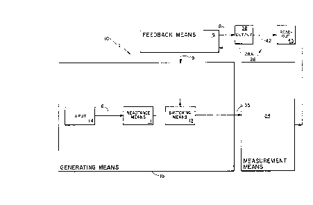
In FIG. 1, a first embodiment of a
measurement circuit i5 indicated generally at 10. An
input 14 provides a signal on line 16 such as a
potential, a current, a pressure, a temperature, a
flow, a pH level, or other variable to be sensed. Line
16, which can comprise multiple signal paths, couples
input 14 to the generating means 18 to provide the
generating means 18 with a signal or signals
1~96~23
representative of the sensed variable. Line 16 of
FIG. 1 can comprise multiple electrical conductors, a
fiber optic cable, pressure passageways or other
coupling means.
Generating means 18 comprises a reactance
mean~ 11, coupled to the input means 14, and a
switching means 13, ~ontrolled by a feedback signal
coupled on line lg from a feedback means 9. The
reactance means 11 is coupled to the switching means 13
for coupling a quantity or number of packets of
electrical charge representative of the sensed
parameter to a measurement means 34 on a line 35. The
term ~packet" refers to a discrete amount of electrical
charge which flows to or from a capacitance when it is
lS charged from a first potential to a second potential,
different from the first potential. The amount of
charge in a packet is proportional to the capacitance
and the difference between the first and second
potentials. The generating means 18 couples first
charge packets having a first polarity and second
charge packets having a second polarity opposite the
first polarity on the line 35 to the measurement means
34. The measurement means 34 accumulates charge by
subtracting the second charge packets from the first
charge packets. When an accumulation of charge in the
measurement means reaches a selected level, a
measurement signal 28 is actuated and coupled back from
measurement means 34 on line 28A to the feedback means
9 to control provision of the feedback signal on the
line 19. The feedforward coupling of the first and
second charge packets on line 35 to the measurement
means 3~ and the feedback coupling of the measurement
~ Z96923
~ 4-
signal on line 28A and the feedback signal on line 19
to the generating means 18 causes a cyclic operation of
the measurement signal 28. In response to an actuation
of the measurement signal on line 28A, the feedback
means 9 actuates the feedback signal on line 19 which,
in turn, actuates switching means 13 to provide a
charge packet or packets representat~ve of the sensed
parameter to the measurement means 34 on llne 35. The
first charge packets coupled on line 35 increases the
accumulation of charge in measurement means 34. The
second charge packets coupled on line 3S reduce the
accumulation of charge in the measurement means 34.
The second charge packets can have a substantially
fixed amplitude or can alternatively be representative
of the sensed parameter. When the charge accumulated
in the measurement means 34 is thus balanced over time
to a selected level, the measurement means 34 again
actuates the measurement signal 28. A quantity or
number of packets of charge needed to return the
accumulation to the selected level is representative of
the parameter. There is a charge balancing interaction
between the generating means 18, the measurement means
34 and the feedback means 9. A quantity or number of
charge packets of the first polarity unbalance the
accumulation of charge in the measurement means 34 and
then a quantity or number of charge packets of the
second polarity are applied to the measurement means 34
until the charge in the measurement means is brought
back into balance at the selected level at which point
the measurement signal 28 is actuated. The quantities
or numbers of charge packets of the first and second
polarities is representative of the sensed parameter.
129~ 3
The accumulation of charge in the measurement means 34
is preferably continuous and not periodically zeroed.
Thus an accumulation of charge packets which exceeds
the amount required to balance the accumulation in the
S measurement means 34 is carried forward to the next
measurement interval. This carrying forward of charge
improves accuracy over several measurement cycles. A
long term average value of the number of charge packets
tends toward an accurate value representative of the
sensed parameter because small accumulations of charge
packets in the measurement means 34 are not zeroed out
and lost at the end of a measurement period, but are
instead carried forward to affect a succeeding
measurement interval~
lS An output signal indicative of the number of
first and second charge packets provided over time is
coupled on line 8 to an output means 38 which couples a
signal representative of the parameter to a readout
means 43 along line 42. Control of the output means 38
is thus a function of the quantity or number of packets
of charge which is representative of the parameter.
The output means 38 can simply couple the outpu~ signal
on line 18 to the readout 43, thereby providing a
signal on line 42 representative of the parameter.
Alternatively, the output means 38 can receive the
output signal on line 8 and be a means for producing an
analog output, a serial dig~tal output, or a combined
analog and digital output.
In FIG. 2, an embodiment of a capacitive
pressure transmitter correspondlng to FIG. 1 is shown.
Reference numbers in FIG. 2 that are the same as the
reference numbers in FIG. 1 identify corresponding
features.
lZ96~23
In the embodiment of FIG. 2, a capacitive
pressuee transducer 14A senses a pressure P indicated
at 1~ and provides variable capacitor 15 having a
capacltance C~ and a variable capacitor 13 having a
capacitance CL each representative of pressure. The
generating means 18 receives signals El and E2 from a
feedback means 9 for controlling switches 100 and 102
to provide excitation to the sensor 14A.
The input 14 is coupled to the generating
means 18 by line 121 to provide a signal representative
of the sensed pressure P to generating means 18. An
excitation logic circuit 104, a bias logic clrcuit 108,
and a sensor logic circuit 114 each receive the
measurement signal 28. The circuits 104, 108 and 114
lS provide signals El, E2, B, Sl and S2 to the control
inputs or gates of switches 100, 102, 106, 116 and 118
respectively and these switches are preferably MOS
transmission gates. These MOS transmission gates are
designed to have a structure which provides for very
low leakage currents when they are open and which
transfers a minimal anount of parasitic charge from the
gate when switched. Desired MOS transmission gate
characteristics are a leakage current of less than 1
pico ampere in an ~off~ state and a charge transfer of
2S less than .05 pico coulombs when switched. Each of the
switches is closed to couple signals by application of
a high or ~1~ level, and is opened to stop coupling
signals by application of a low or "0" level to the
control input or gate of the switch. Switches 100 and
102 are closed sequentially in a non-overlapping manner
to couple reference potentials +V and -V to transducer
14A providing desired excitation to transaucer 14A.
12969~
Switch 106 is closed periodically to couple the line 17
to DC common reference potentlal 110 through resistance
112 thereby adjusting a DC bias on amplifier 120 to a
desired level. Amplifier 1~0 senses a transducer
signal at a high impedance ~nput coupled to line 17 and
couples a signal representative of the sensed parameter
from a low impedance output 121 to a capacitor 117
having a capacitance Cl. Sensor logic circuit 114 in
feedback means 9 controls switches 116 and 118 to
couple a charge packet representative of the sensed
parameter from capacitor 117 to line 32A. One such
charge packet is generated on line 32A in response to
each actuation of the measurexent signal 28. A flow of
charge on line 32A is thus proportional to the sensed
pressure P, to the number o applications of actuations
of measure~ent ou~put 28, to a reference poténtial
coupled to sensor 14, and to the capacitance Cl.
In feedback means 9, a reference logic
circuit 150 provides signals Rl and R2 for controlling
switcbes 152, 154, 156 and 158 as hown in FIG. 2.
Firstly, switches 154 and 158 are closed thereby
coupling capacitor 153 between reference potentials +V
and DC co~mon and storing a charge on a capacitor 153
having a capacitance C2 while switches 152 and 156 are
open. Secondly, switches 152 and 156 are closed
coupling capacitor 153 between reference potential -V
and line 36 while switches 15~ and 158 are open and a
packet of charge is thus discharged into line 36A.
This switching sequence is continuously repeated to
provide an average flow of charge or current on line
36A proportional to a reference potential, to the
capacitance C2 of capacitor 153 and, to the frequency
of the actuation of switches 154 and 158.
1296923
The first signal on line 32A and the second
signal on line 36A in FIG. lB are of opposite polarity
so that the first signal charges an integrator 160 in a
first direction and the second ~lgnal charges the
s integrator 160 in a second direction opposite the first
direction. The two signal on lines 32A and 36A are
effectively subtracted at the integrator 160 because
they have opposite polarities. The integrator 160
comprises an amplifier 162 having high impedance inputs
163 and 165 and an integrator capacitor 164 coupling
between an output 168 of amplifier 162 and the
inverting input 163 of amplifier 162. A noise bypass
capacitor 166 is coupled from the inverting input 163
to a non-inverting input 165 of amplifier 162 which is
also coupled to DC co~mon 110. The integrator 160
accumulates charge packets coupled on lines 32A and 36A
and provides an integrator signal at integrator output
168 that is representative of the charge accumulated.
Integrator signal 168 is coupled to an inverting input
169 of comparator 170; a non-inverting input of
comparator 170 is coupled to a reference potentlal,
preferably DC common 110. The comparator 170 compares
the level of ~he integrator signal 168 to the reference
potential 110 and provides the mea~urement signal 28 to
2s line 28A indicative of the polarity of integrator
signal 168 with respect to the reference potential 110.
A flow of charge Ql in the first signal 32 on
line 32A is substantially
Ql = (Nl)(Cl)(VR) fl - CH-CL~ Eq. 1
2 ~ CH+CL/
where:
Ql is a total flow of charge on line 32A during a
time interval T;
lZ969Z3
Nl is the quantity or number of charge packets on
line 32 in the time interval T;
Cl is the capacitance of capacitor 117;
VR is the potential difference between reference
potentials +V and -V applied to switches 100 and
102;
CH is a capacitance of pressure sensing capacitor 15;
and
CL is a capacitance of pressure ~ensing capacitor 13.
The flow of charge Q2 on line 36A is
substantially
Q2 ~ (N2)(C2)(VR) Eq. 2
where:
Q2 is a total flow of charge on line~36A during the
time interval T;
N2 is the quantity or number of charge packets on
line 36 during the time interval T;
F2 is a fre~uency at which circuit 150 actuates
switches 152 and 156;
C2 is the capacitance of capacitor 153; and
VR is the potential difference between reference
potentials +V and -V applied to switches 152 and
154.
The lntegrator 160 is repetitively rebalanced
2s so that no net charge accumulates on the integrator
over a series of cycles of the measurement signal 28
during the time interval T. ~ence, the charge Ql is
controlled to equal substantially the charge Q2.
Combining the above equations 1 and 2 for Q~ and Q2,
with Ql = Q2 discloses the following relationship:
1296~323
-10-
N2 = (Nl) (Cl) (1 - CH-CL~ Eq. 3
2 (C 2 ) CH+CL J
The Equatlon 3 above shows that N2 is
substantlally dependent only on capacitances and the
number of charge packets Nl. The number Nl can be held
constant by counting the number of pulses N2 over a
constant number Nl of pulses making N2 a function of CH
and CL. Both signals 32 and 36 are proportional to the
same reference potential VR, but this reference
potential term VR is cancelled out in the above
equation 3 defining a number of charge packets that is
substantially independent of the reference potential
over an operating range. Capacitances Cl and C2 can be
selected to have substantially matched temperature
characteristics, so that variations with temperature of
Cl in the numerator are cancelled out by similar
variations with temperature of C2 in the denominator of
the above equation making the num~er of pulses N2
insensitive to the temperature of transmitter
circuitry. The number of pulses N2 is also
substantially independent of the selected level applied
to the comparator over an operating range. Hence, the
selected level can be the reference potential -V
instead of the DC common level shown when amplifiers
120, 162 and comparator 170 are designed to operate at
levels near the -V reference potential. The term (~CH
-CL)/(CH+CL) ) in the above equation is proportional to
the pressure P applied to transducer 14A. Hence it can
be seen that the number N2 is dependent on the pressure
P and can be substantially independent of the reference
potentials and ambient temperature of the transmitter
over an operating range.
lZ~6~23
In FIG. 3, timing relatlonsh~ps between the
integrator signal 168, the measurement signal 28 and
the signals El, E2 , B , Sl, S2 of FIG. 2 are shown in a
timing diagram 178. A first axis 180 represents time
starting from a time T0 shown at 182. A second axis
18q represents a level 186 of the integrator signal 168
and a selected level 188 applied to the non-inverting
input 171 of comparator 170. The application of
packets of charge from line 36A to the integrator 160
causes the integrator signal level 186 to be stepped in
a negative direction until the integrator signal level
186 resches the selected threshhold level 188 at time
T0 at 182. Comparator 170 senses that the integrator
signal level 186 has reached the selected threshhold
level 188 and actuates the measurement signal on line
28A as shown at 192 in FIG. 3. The measurement signal
on line 28A actuates the circuits 104, 108, and 114 to
provide signals El, E2, B, Sl and S2 as shown in
FIG. 3. Firstly, signal E2 is actuated as shown at 194
to close switch 102 and discharge the series
combination of pressure sensing capacitor~ 13 and 15.
While sw~tch 102 is closed, signal B is actuated as
shown at 193 to close switch 106, adjusting the bias at
the junction of capacitors 13 and 15 to substantially
the DC common level 110. Signal S2 shown at 198 has
held switch 118 closed durlng this time to charge
capacitor 117 to a fir6t level of a signal on line 121.
After switches 102, 106 and 118 are opened, siqnal El
is actuated as shown at 196 to charge the series
combination of pressure sensing capacitors 13 and 15 to
the reference potential. The series combination of
capacitor 13 and 15 operates as a capac~tive potential
1296~323
-i2-
divider and the potential prov~ded by the ~ensor 14A on
conduc~or 17 is determined by pressure sensitive
capacitances CH and CL and hence the potential on
conductor 17 is representat~ve of pressure. Amplifier
120 provides a buffered output to capacitor 117
substantially equal to the potential on conductor 17.
Finally, signal Sl closes switch 116 as shown at 202
and a packet of charge representative of the parameter
flows on line 32A to the integrator 160 from capacitor
117. The flow of charge on line 32A may be seen as a
flow of positive charge from the integrator 160 to the
capacitor 117 or alternatively may be seen as a
negative flow of charge from the capacitor 117 to the
integrator 160. The integrator output level ls
increased as shown at 204 by the application of the
charge packet from the line 32A. ~his application of
charge from the line 32A is then balanced out by
- application of charge from the line 36A until time Tl
shown at 206 when the measurement signal is again
actuated as shown at 208 and the cycle is repeated.
In FIG. 4, an embodiment of output means 38
corresponding to FIG. 2 is shown. Output means 38
receives signals on line 8 representative of the
numbers Nl and N2 and provides a transmitter output
2s signal to an output bus 42 compatible with a
standardized serial digital data bus. In the
embodiment shown in FIG. 4, the feedback means 9
provides a pulse signal representative of the quantity
or number (Nl+N2) of charge packets of both polarities
to line 8B and a pulse slgnal representative of the
number Nl of charge packets of the first polarity to
line 8B.
lZ96~23
-13-
In FIG. 4t the signal on llne 8A is coupled
to a divide-by-N co~nter 250 whlch provides a gating
signal 252 having a period longer than the signal on
line 8B. The gating signal 2S2 is applied to a gating
input 256 of a counter 254 to gate counting of the
slgnal on line 8B applied to a clocking input 258 of
the counter 254. The counter 254 provides a multibit
digital word on a parallel data bus 260 which is
representative of the sensed pressure. The digital
word on the data bus 260 is accepted by a first
parallel input port 262 of shift register 26~. A
control logic c~rcuit 266 receives a data clock signal
on line 268 and a chip select signal ~CS~ on line 270
from the output bus q2. A memory 272 is a laser
programmed memory which is programmed to contain data
characterizin~ the sensor 14A and the transmitter lO.
Such characterizing data may include linearity
constants, identification numbers, and span and zero
temperature coefficients of the sensor 14A. Data
stored in memory 272 is transferred via parallel bus
274 to a second parallel input port 276 of shift
register 264. When actuated by a signal on chip select
line 270, the control logic circuit controls memory 272
via line 280 and counter 254 via line 282 to provide
parallel data representing the sensed parameter and the
characterization data to shift register 264. Control
logic circuit 266 then controls shift register 264 via
line 284 to shift the data in the shift register
serially out on line 286 in synchronization with the
data clock signal on line 268. A serial aata word is
coupled out on line 286 which contains data
representative of the sensed parameter and data
1296!3;~:3
-14-
representative of the characterization constants stored
in memory 272.
Lines 288 and 290 provide a 5 volt supply and
reference potential from the data bus to the
transmitter. Bandgap reference 292 is energized from
lines 288 and 290 to provide a DC commom reference
potential ll0 to circuitry in transmitter l0.
Substantially all of the circuitry of transmitter l0 is
fabricated as an MOS integrated circuit to provide
desired low power consumption. Transmitter l0 is
preferably energized by a two-wire, 4-20 mA industrial
control current loop. Lines 268, 270, 286, 288 and 290
comprise a 5-wire output bus 42 compatible with a
microprocessor-based, loop-powered instrument.
In FIG. S, a circuit 300 is shown which can
couple via lines 270, 268, 286, 288 and 290 to the five
wire output bus 42 shown in FIG. 4. Circuit 300
together with the circuit of FIG. 4 can comprise an
output means for providing an analog output or a
combined analog and digital output. A computing means
302, preferably comprising a microcontroller type
COP444C manufactured by National Semiconductor
Corporation, receives a serial data word at a serial
inpu~ 304 from line 286 of data bus 42 in response to
actuation of chip select line 270 by the computing
means 302 and in synchronization with the data clock
signal on line 268. A clock means 306, a memory means
308 and a timer means 310 are coupled to the computing
means 302 to support operation of the computing means.
Memory 308 comprises a non-volatile memory storing
alterable constants which control transmitter
characteristics such as span and zero, or sensor
1296923
-l5-
characteristics received from memory 272 of FIG. 4.
Timer 310 is a so-called ~watchdog~ timer which senses
when computing means 302 has ceases to provide a signal
indicative of normal operation for a selected timed
interval and provides a reset siqnal to the computing
~eans 302 when such failure occurs. Switch 312 can be
manually actuated to provide a signal to computing
means 302 setting a transmitter output characteristic
to a ~zero" level. Switch 314 can be manually actuated
to provide a signal to computing means 302 setting a
transmitter output characteristic to a full scale or
~span" level. Display 316 is connectable to computing
means 302 to receive and display data from computing
means 302, particularly a current value of the sensed
parameter 12. Clock 306 preferably comprises a crystal
oscillator for clocking the operation of computing
means 306 and other portions of the output circuit.
A data word representative of the sensed
parameter received from line 286 and constants stored
in memory means 308 are input data to computing means
302 for computing an output word representative of the
sensed parameter. The output word representative of
the sensed parameter i5 coupled by the computing means
from its serial outpu~ 316 to digital-to-analog
converter 318 along line 320. Computing means 302
selects converter 318 to receive the output data word
by actuation of a chip select output on line 322. The
clock 306 is coupled to the converter 318 via line 324
and the data clock signal from computing means 302 is
also coupled to the converter 318 via line ~68 to
support operation of converter 318. The converter 318
preferably comprises a type 9706 manufactured by
1~96.9;23
Fairchild semiconductor. Converter 318 couples an
analog output representative of the sensed parameter on
line 326 to regulator circuit 330. Regulator circuit
330 receives the analog output representative of the
sensed parameter on line 326 ~nd controls a 4-20 mA
output current representative of the sensed parameter
at terminals 332 and 334. The regulator circuit 330 i8
excited by the 4-20 mA output current and provides a
regulated 5 volt supply and reference potential on
conductors 288 and 290 for energizing the circuitry
shown in circuit 300 and the circuitry shown in FIGS. 2
and 4.
The 4-20 mA output current at terminals 332
and 334 is energized by an energization source 336
connected in series with a current readout means 338 as
shown in FlG. 5.
The computing means 302 can also couple to an
ACIA or asynchronous communication interface adapter
340 via lines 342 to provide two-way digital
communication between the computing means 302 and a
digital communications device 344 which is connectable
to the 4-20 mA current loop as shown in FIG. 5. The
ACIA preferably comprises a type ~D63S0 manufactured by
Hitachi. The ACI~ 340 couples a serial data word along
line 346 to a modulator which provides an FSK or
frequency shift keyed serial output coupled on line 350
to the regulator circuit 330. The regulator circuit
superimposes the FSR signal on the 4-20 mA output at
terminals 332 and 334. The FSR serial signal is then
30 coupled along lines 352 and 354 to a device 344 which
demodulates and decodes the serial siynal to provide a
readout of data from computing means 302. The FSR
lZ~2~
-17-
signal superimposed on the output current loop i8
selected to have a high enough modulation frequency and
a low enough amplitude compared to the 4-20 mA signal
such that it does not substantially lnterfere with
current measurement in the current loop.
The device 344 can also couple ~ FSR serial
data signal representative of a command from serial
communication device 344 along lines 352 and 354 to the
regulator 330. This signal representa~ive of a command
is then coupled from regulator 330 ~o demodulator 360
along line 362. Demodulator 360 demodulates the
command signal and provides a serlal command signal to
the ACIA 340 along line 364. The ACIA 340 receives the
serial command signal from line 364 and provides this
command to computing means 302 via bus 3~2. The
command signal received from device 344 can be used by
computing means 302 to alter the operation of the
transmitter 10.
In FIG. 6, an alternate embodiment of the
circuitry shown in FIG. 2 is shown. Reference numbers
in FIG. 6 that are the same as reference numbers in
FIG. 2 identify correspondinq features. In FIG. 6, a
sensor 14 comprises a resistive bridge transducer
circuit 380 of conventional design responsive to the
process parameter 12. Resistive bridge circuit 380 can
comprise a strain gauge pressure sensor sensing a
process pressure which can be alternatively a gauge
pressure, an absolute pressure or a differential
pressure. Alternatively, bridge circuit 380 may
comprise a resistive bridge comprising a temperature
sensitive resistor for sensing a process temperature.
Bridge circuit 380 is excited by switches 382, 384, 386
1296923
and 388 which connect the bridge circuit to the supply
potential +V and -V via conductors 390 and 392. The
bridge 380 provides a signal representative of the
sensed parameter coupled on lines 394 and 396 to
amplifier 12Q. A feedback resistance 398 controlling
the gain of amplifier 120 is coupled to amplifier 120
via llnes 396 and 400. The feedback resistance 398 is
preferably disposed adjacent to bridge 380 such that
the feedback resistance 398 and at least a portion of
bridge 380 can be matched in temperature and
temperature coefficient of resistance to minimize
undesired effects of an ambient temperature on the
bridge.
Other portions of the circuitry in FIG. 6
operate analogously as described in connection with
~IGS. 2 and 3 above. A first signal on line 32A is
generated and provides a packet of charge
representative of the sensed parameter in response to
each actuation of a measurement signal 28. A second
signal on line 36A is generated and provides packets of
charge as con~rolled by the feedback means 9.
Measurement means 34 in FI~. 6 accumulates charge from
lines 32A and 36A and provides a measurement signal on
line 28A representative of the sensed parameter 12.
Measurement signal 28 is coupled on line 28A back to
feedback means 9 in FIG. 6 to control generation of
charge packets on line 32A.
In FIG. 7, an embodiment of a transmitter is
indicated generally at 50. A parameter 52 such as a
pressure is coupled along a passageway 56 to sensor 54.
The sensor 54 can be disposed in transmitter 50 or
alternatively can be located remotely from transmitter
50 to provide remote sensing.
~Z36923
~19-
Generating means 58 generates a first signal
72 on line 72A which is representative of the parameter
52. The first signal 72 on line 72A provides charge
packets comprising an amount of charge representative
of the parameter 52 during a fir~t time lnterval
controlled by the feedback means 59. Generating means
58 also generates a second signal on l~ne 76A which is
representative of the parameter 52. The second signal
on line 76A provides charge packets compri ing an
amount of charge representative of the parameter 52
during a second ~ime interval, different from the first
time interval, controlled by the feedback means 59~ A
first packet of charge provided by the first signal 72
has a first polar~ty and the amount of charge in such
first packet increases with an increase in the sensed
parameter 52. A second packet of charge provided by
the second signal 76 has a second polarity, opposite
the first polarity and the amount of charge in such
second packet decreases wlth an increase ~n the sensed
parameter 52.
A measurement means 74 accumulates charge
from the signals on l~nes 72~ and 76A. When the
accumulation of charge from the first signal on line
72A in the measurement means 74 increases to a first
2s selected level during the first time interval, the
measurement signal 68 on line 68A is actuated in a
first direction. The measurement signal 68 is coupled
back to the feedback means 59 and the feedback means 59
responds to such actuation by ending the first time
interval and starting the second time interval. During
the second time interval, the measurement means 74
accumulates charge from the second signal 76 until the
12969Z3
-20-
accumulation of charge decreases to a second selected
level, different from the first selected level. When
the second selected level is reached, the measurement
signal 68 is actuated again in a second dlrection
S opposite the first direction. The actuation in the
second direction is sensed by the feedback means 59 and
the feedback means 59 responds to such actuation by
ending the second time interval and starting another
first time interval.
The feedforward coupling of signals on lines
72A and 76A from the generating means 58 to the
measurement means 74 and the feeaback coupling of the
measurement signal 68 to the feedback means S9 and the
generating means ~8 causes a cyclic operation of the
measurement signal 6~. The qenerating means S8 and the
feedback means 59 and the measurement means 74 operate
together in a closed loop configuration to provide
quantities or numbers of charge packets which are
representative of the sensed parameter.
In FIG. 7, feedbck means 59 comprises digital
circuitry which receives the measurement signal 68 and
provides pulsed signals on lines 60 and 61 that are
representative of the numbers or quantities of charge
packets provided by the generating means ~8. Pulsed
signal 60 provides pulses during the first time
interval. Pulsed signal 6l provides pulses during the
second time interval.
Output means 78 receives the pulsed signals
60 and 61 and counts a number of pulses received from
signal 60 during a measurement time interval controlled
by a total number of pulses received from both signals
60 and 61. ~he number of pulses thus counted is
-21-
representa~ive of the sensed parameter, and output
means 78 prov~des an ou~put signal 82 on line 82A
compri~ing a signal representative of this courlt of
pulses and thus the parame~er. The output 82 i~
5 coupled to a re~dout 83 which indicates a curr~nt value
of the sensed para~e~er 52.
In FIG. 7, the capacitive sensor 54 co~prises
capacitances 53 and ~7 dependent on the applied
pressure P at S2. A feedback means 5g comprises an MOS
10 digital logic circuit which receives the measurement
slgnal 68 and controls switches 421 and 423 to couple
an excita~ion signal CXO ~o the sensor 54 along line
410. The excitation signal CKO from line 410 ls
generated from switches 421 and 423 coupled to the
reference potentials ~V and -V as shown in a timing
diagram shown in FIG. 8~ and has an amplitude
substantially equal to a reference po~ential shown at
~12. An ;nverter 414 receives the signal CRO on llne
410 and generates an inverse signal CKO which is
20 coupled to linearity correction c~pacitances 4l5 and
417 along line 416. Referring now to FIGS. 7 and 8~
the feedback means 59 also produces signals CKl, CR2,
CR3 and CR4, as shown, for controlling actuation o~
switches 422, 424, 418 and 420 respectively and these
25 switches are preferably MOS type swi~ches as described
above.
While the excitation signal CRO is at a lower
level as shown at 426 in FIG. ~, and the excitation
signal CKO is a~ a high level as shown at 427, the
signal CK3 is actuated for a time as shown at 428 to
close swltch 418 to conduct, ~hereby storing desired
charges on sensing capacitance 57 and linearity
correction capacitance 417.
12969Z3
-22-
While the excitation signal CKO is at a
higher level as shown at 430, and the excitation signal
CKO is at a lower level as shown at 431, the signal CK4
is actuated for a time as shown at 432 to close switch
S q20, thereby storing des$red charges on sens1ng
capacitor 53 and linearity correction capacitor 415.
The timinq of signals CKO, CKO, CR3 and CR4 is
substantially independent of the measurement signal 68.
The pressure sensing capacitors 53 and 57 are
excited by signal CRO which has a 180 degree phase
relationship with the signal CRO which excltes the
linearity correction capacitors 415 and 417. This
phase relatioship allows for compensation for undesired
stray capacitance associated with pressure sensing
capacitors 53 and 57. Capacitor 415 has a selected
capacitance CLl and i5 excited to subtract a selected
quantity of charge from capacitor 53. Capacl~or 417
has a selected capacitance CL2 and is excited to
subtract a selected quantity of charge fro~ capacltor
57. The quantity (CL2-CLl) is adjusted to reduce
second degree non-linearity the relationship between
sensed pressure and the quantity (CH-CL)/(CR~CL). The
quantity (CL2+CLl) is adjusted to reduce third degree
non-linearity in the relationship between sensed
pressure and the quantity (CH-CL)/(CH~CL). The
linearity of the transmitter output is thus improved.
The group of timing waveforms 4g8 of the
timing diagram in FIG. 8 is representative of an
example where an applied pressuse P is substantially
zero and the capacitance CH is substantially equal to
the capacitance CL. While the mea~urement siqnal 68 is
coupled to feedback means 59 at a first level 434
lZ963%3
during the first time interval, circuit S9 repetitively
actuates siqnal CRl as shown at 436 to close switch 422
and couple charge packets from senslng capacitor 53
corrected by linearity correction capacitor 415 to the
S line 72A. While the measurement signal is coupled to
the feedback means 59 at a second level during the
second time interval as shown at 438, circuit 59
repetitively actuates s$gnal CR2 as shown at 440 to
close switch 424 and couple charge packets from sensing
capacitor 57 corrected by linearity correction
capacitor 417 to the line 76A.
The measurement means 74 comprises an
integrator 442 which accumulates charge from the first
and second signals during first and second time
intervals respectively and provides an integra~or
signal 444 representative of the accumulated charge.
Integrator signal 444 is coupled to an input of a
Schmidt trigger or comparator 446. Schmitt trigger 446
has hysteresis between selected upper and lower
triggering levels. Schmitt trigger 446 provides the
measurement signal 68 on line 68A which is fed back to
control feedback means 59 and charge generating means
58.
In FIG. 8, the level 441 of integrator output
444 is shown to increase as charge packets of a first
polarity from the first signal 72 are applied during
the first time interval until it passes the fisst
selected level 443 ending the first time interval and
starting the second time interval. The level 441
decreases as charge packets of a second polarity
opposite the first polarity are applied to the
integrator 442 during the second time interval.
~Z96~23
-24-
When capacitance CL is approximately equal to
three tlmes capacitance C~ as shown by ano~her example
in the group of timing waveforms 450 however, three
times as many pulses 352 occur on line 61 as occur on
s line 60. The signals on line 60 and 61 are derived
from the ~easurement sign~l 68 by the operation of
feedback ~eans 59.
A flow of charge from the first signal 72 per
cycle of the measurement output is
Ql - (Nl)(CH-CLl)(V) Eq.
wbere:
Ql is the ~uantity of charge supplied by the fir~t
charge output during one cycle of me~surement
output 68:
Nl is the count or number of packets of charge
provided by the first signal during one cycle of
that the measurement output;
CH is the sensor capacitance CH and
v is the reference potential.
~ flow of charge from the second charge
output 76 per cycle of the mea~urement signal is
Q2 = (N2)(CL-CL2)(V) Eq. 5
where:
Q2 is the quantity of charge supplied by the second
2S signal during one cycle of neasurement ouput 68;
N2 is the count or nu~ber of charge packets provided
by the second signal during one cycle of the
measurement signal;
CL is the sensor capacitance CL; and
V is the reference potential.
The equations 4 and 5 for charge quantities
Ql and Q2 are approximations which do no~ take into
1296;9%;~
account a ~least count~ error in counting pulses.
However, over a large number of measurement cycles,
such least count errors tend to cancel out one another.
The integrator is never zeroed and; hence, portions of
charge packets that drive the integrator beyond a
selected leYel of the Sch~itt trigger are carried over
to the next time interval. With this carry over of
charge, the summation of charges Ql equal substantially
the summation of charges Q2 over a long time interval T
comprising many measurement cycles and; hence,
(Ml ) (CH ' ) - (M2 ) (CL ' ) Eq. 6
where:
CH' is the corrected capacitance (CH-CLl);
CL' is the corrected capacitance (CL-CL2);
Ml is tbe number of pulses on line 60 which is also
the number of charge packets generated by the
first signal during time interval T; and
M2 is the number of pulse on line 61 which is also
the number of charge packets generated by the
second signal during time interval T.
Terms in equation 6 can be rearranged to define a first
output equation Equation 7: ~
M2 S (1/2) (Ml+M2)~1 + CH~-CL' Eq. 7
~ CR'~CL'
Terms in equation 6 can also be rearranged to define a
second output equation Equation 8:
M2--Ml = (Ml+M2) (CR'--CL' ) Eq. 8
(C~'+CL' )
Equation 7 or Equation 8 can be used in an output
circuit 78 as explained below.
1:Z'3692.~
-26-
In FIG. 9, an output circuit 78 which
corresponds to FIG. 7 is shown. The output circuit 78
comprises a counter control logic circult 460 which
receives the previously described pulses on lines 60A
and 61A and is coupled to counter 466 to control pulse
counting by counter 466. The counter 466 is gated to
count pulses in a time interval during which a selected
number of pulses (Ml+M2) corresponding to the selected
ti~e interval T are received from lines 60 and 61.
In one preferred e~bodiment, the counter 466
counts the number of pulses M2 received from line 61A
during the time interval. The number of pulses (Ml+M2)
is set to a selected value, for example, 200,000
pulses, by the counter control logic 460 and; hence,
lS the count M2 is related to the sensed pressure by
Eq. 7. ~his counting is preferred for providing a
count which is representative of an unsigned pressure
variable such as a pressure which varies from zero to a
full scale value.
In yet another preferred embodiment, the
counter 466 is an UP/DOWN counter and counts the
difference in counts (M2-Ml) during the time interval
T. The nu~ber of counts (M2~Ml) is set to a selected
value, for example, S0,000 by the counter control loglc
460 and, hence, the count (M2-Ml) is related to the
sensed pressure by Eq. 8. This counting is preferred
for providing a count which is representative of a
signed pressure or variable which varies from a
negative full scale value to a positive full scale
value.
The count in counter 466 is representative of
the sensed parameter and is transferred on parallel bus
~29~'32;3
468 to a shift register 470. Shift register 470 also
receives data from a parallel bus 472 characterlzing
the sensor 54 which has been previously stored in a
memory 474. A five-wire output data bus 82 couples a
chip select or CS signal on line 476 and couples a data
clock signal on line 47~ both to a control logic means
480 which controls provision of parallel data from
memory 474 and counter 466 to shift reglster 470.
Control logic means 480 also controls shift register
470 to provide a serial output of the data in the shift
register to line 482 of the output bus, synchronous
with the data clock on line 478.
The output bus 82 provides a 5 volt reference
to the transmitter along lines ~8~ and 486 and a MOS
voltage divider 488 provides a DC common reference
level 490 to the transmitter. The five-wire output bus
of FIG. 9 may be coupled to a circuit such as the
circuit shown in FIG. S to provlde a 4-20 mA analog
output and digital output to a two-wire loop.
Transmitter circuitry preferably comprises a
custom MOS integrated circuit to provide a desired low
cost, compact transmitter.
In FIG. 10, an e~bodiment of a measurement
circuit 500 is shown. Measurement circuit 500 sense~
an input signal from a potent~al source 510 and
provides a signal on line 512 to a readout means 514 as
a function of the sensed potential on line 514.
Potential source 510 is coupled to a generating means
510. Generating means 520 comprises a capacitor 522
which is a reactance means having a capacitance C. The
capaci~or 522 is coupled to the input signal on line
514 through a switch 524. A switch 526 couples the
lZ96~
-28-
capacitor 522 to a reference potential 528; sw~tches
530 and 532 couple the capacitor 522 to a second
reference potential 110 which can be a DC common level.
A switch 534 co~ples the capacitor 522 to line 536 to
provide a generator signal responsive to the sensed
input signal. Switches 524, 526, 530, 532, and 534 are
controlled by digital signals CK2, CK3, CK5, CK4 and
CKl respectively which are feedback signals coupled
from the feedback means 538. A measurement means 540
receives and measures the generator signal coupled on
line 536. Integrator means 542 accumulates charge
received from line 536 and provides an integrator
signal on line 544 which is coupled to a comparator
546. The comparator 546 compares the integrator signal
to a reference potential 110 and couples a measurement
signal to line 548 which is a function of the charge
coupled to the measurement signal to line 548 which is
a function of the charge coupled to the measurement
means on line 536. Line 548 is coupled to the feedback
20 means 538 for controlling the feedback means 538. ~he
feedback means 538 produces and couples the digital
feedback signals CKl, CK2, CK3, CX4 and CK5 to the
generating means 520. Feedback means 538 also couples
digital output signals CK6 and CK7 on lines 550 and 552
respectively to an output means 554 which counts pulses
on lines 550 and 552 to provide a signal on line 512
which is a function of the sensed voltage on line 514.
In FIG. 11, a timing diagram S80 shows timing
relationships between the measurement signal which
control the feedback means 538 and the feedback signals
CKl, CK2, CK3, CR4 and CK5 which are produced by the
feedback means. FIG. 11 also shows the timing
lZ96i~Z~3
-29-
relationships between the feedback signals, the
integrator signal VI, and the measurement signal VS.
Before the start of the tlmlng sequence shown in
FIG. 11, the switches 530 and 532 have been closed to
S discharge the capacitor 522 to substantially a zero
potential. At 528 in FIG. 11, signals CRl and CR2 are
actuated to couple the capacitor 522 to the input
potential on the line 514 and the generator output on
line 536, thus coupling a packet of charge
representative of the sensed voltage to the measurement
means 542. The ~ntegrator 542 receives this packet of
charge and the integrator output VI increases above the
reference potential V~ as shown at 584. Next, signals
CK3 and CRS are actuated as shown at 586 to close
switches 526 and 530, thus charging capacitor 522 to
~he reference potential +V at 528 in FIG. 10. The
signals CRl and CX4 are then actuated as shown at 588
to couple a packet of charge as a function of the
reference voltage 528 to the measurement means S40 on
line 536. ~he signals CR3 and CRS are actuated again
as shown at S90 to again charge capacitor 522 to the
reference potential, and the signals CKl and CR4 are
again actuated as shown at 592 to discharge another
charge packet as a function of the reference 528 into
the measurement means on line 536. The process of
charging capacitor 522 to the reference potential and
then discharglrg the charge packet into the line 536 is
repeated until the integrator output drops below the
reference voltage VT as shown at 594. When the
integrator signal drops below the reference potential
YT, the measurement output changes as shown at 596,
thus triggering the feedback means to discharge the
i9~;~
-30-
capacitor 522 as shown at 598 and couple another packet
of charge representatlve of the sensed parameter into
the measurement means 540 as shown at 600 in FlG. 11.
The number of charge packets representatlve
of the sensed parameter which are provided on 11ne 536
is represented by a number of pulses Nl whlch are
produced in s~gnal CR6 on line SS0. The number of
charge packe~s as a function of the reference potential
which are provided on line 536 is represented by a
lo number of pulses N2 which are produced in signal CR7 on
line 552. The numbers Nl and N2 are related to one
another since (Nl)(C~(V)=(N2)(C)(VR) by the following:
V = (N2/Nl)(VR)
where:
V is the input potential on line 514
VR is the reference potential 528
Nl is the number of pulses on line 5S0 during a time
interval, and
N2 is the number of pulses on line 552 durlng the
time interval.
~ence, it can be seen that counting pulses on
lines 550 and 552 by an output means such as the one
described in connection with FIG. 9 can provide an
output 512 which is representatlve of the sensed
potential on line S14. The circuit 500 can be used ac
an analog-to-digital converter circuit for interfacing
an analog signal to a digital readout means 514.