Note: Descriptions are shown in the official language in which they were submitted.
~97~
RCA 84,745 "
VIDEO SIGNAL PROCESSO~ WITH
ALTERNATE suscARRIER
This invention concerns a widescreen television
system that is compatible with conventional television
S receivers having a relatively smaller display aspect ratio.
More specifically the present invention relates to a method
and apparatus for encoding and/or decoding a video signal
in such a system.
A conventional television receiver, such as a
receiver in accordance with NTSC broadcast standards
adopted in the United States and elsewhere, has a 4:3
aspect ratio (the ratio of the width to the height of a
displayed image). Recently, there has been interest in
using higher aspect ratios for television receiver systems,
such as 2~1, 16:9 or 5:3, since such higher aspect ratios
more nearly approximate or equal the aspect ratio of the
human eye than does the 4:3 aspect ratio of a conventional
television receiver. Video information signals with a 5:3
aspect ratio have received particular attention since this
ratio approximates that of motion picture film, and thus
such signals can be transmitted and received without
cropping the image information. However, widescreen
television systems which simply transmit signals having an
increased aspect ratio as compared to conventional systems
are incompatible with conventional aspect ratio receivers.
This makes widespread adoption of widescreen systems
difficult.
It is therefore desirable to have a widescreen
television system that is compatible with conventional
television receivers. In accordance with the principles of
the present invention, there are disclosed herein method
and apparatus for encoding and decoding a compatible
widescreen video signal representing a picture having an
aspect ratio greater than the standard 4:3 aspect ratio.
A disclosed preferred embodiment in accordance
with the principles of the present invention includes
apparatus for encoding a video signal. Means for
generating a video signal containing information to be
~7~
-2- RCA 84,745
displayed during periodic horizontal line image intervals
which recur at a horizontal line scanning frequency. The
video signal comprises a luminance component including
vertical image detail information occupying a first
frequency band, a chrominance subcarrier component
modulated with color image information occupying a second
frequency band, and information representative of a given
characteristic of an image to be displayed. Means are
included for providing an alternate subcarrier signal with
an interlaced frequency between the first and second
frequency bands. Also included are means for modulating
the alternate subcarrier signal with the representative
information to produce a modulated alternate subcarrier
signal with a bandwidth in accordance with the
representative information.
In a further aspect of the present invention, the
video signal generated includes a widescreen signal having
left side, right side and center video information panels.
The given characteristic of the image to be displayed
includes high frequency side panel information. The high
frequency side panel information is encoded by modulating
such high frequency information on an alternate subcarrier
signal other than the chrominance subcarrier.
In still a further aspect of the invention, the
~5 alternate subcarrier is preferably at an interlace
requency which is an odd multiple of one-half the
horizontal line rate, and is located between the luminance
vertical detail band and the chrominance band.
In yet another aspect of the invention, a video
signal processing apparatus is provided which includes
means for demodulating the modulated alternate subcarrier
signal.
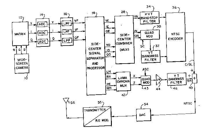
Figure 1 shows a block diagram of an encoder for
a compatible widescreen television system in accordance
with the principles of the present invention;
Figures 2 - 5 depict signal waveforms helpful in
understanding the operation of the system of Figure l;
- 12~7~B
-3- RCA 84,745
Figures 6 - 10, 12 and 12a - 12d illustrate
aspects of the system of Figure 1 in greater detail;
Figures lOa - lOc illustrate aspects of filter
arrangements related to a filter network shown in Figure
10;
Figure 11 depicts an amplitude versus frequency
response characteristic associated with a feature of the
system of Figure l;
Figure 13 shows a block diagram of a portion of a
widescreen television receiver including decoder apparatus
in accordance with the present invention; and
Figure 14 shows a portion of the decoder of
Figure 13 in greater detail.
A brief overview of the system to be described
will be helpful. A sys em intended to transmit wide aspect
ratio pictures, e.g., 5:3, through a standard, e.g., NTSC,
channel should achieve a high quality picture display by a
widescreen receiver, while greatly reducing or eliminating
observable degradations in a standard 4:3 aspect ratio
display. The use of signal compression techniques on the
side panels of a picture takes advantage of the horizontal
overscan region of a standard NTSC television receiver
display, but may sacrifice image resolution in the side
panel regions of a reconstructed widescreen picture. Since
compression in time results in an expansion in the
frequency domain, only low frequency components would
survive processing in a standard television channel, which
exhibits a smaller bandwidth compared with that required
for a widescreen signal. Thus, when the compressed side
panels of a compatible widescreen signal are expanded in a
widescreen receiver, there results a noticeable difference
between the resolution or high frequency content of the
center portion of a displayed widescreen picture and the
side panels, unless steps are taken to avoid this effect.
The Figures and associated description describe a
system for developing a widescreen signal capable of being
processed through a standard NTSC channel. The system also
permits a widescreen receiver to recover a widescreen
.. . .... ... ..
7~
-
-~- RCA 84,745
picture with good picture quality across the entire
display.
As will be seen from the encoder of Figure 1, the
use of spatial compression allows low frequency side panel
information to be squeezed into the hori~ontal overscan
region of a standard NTSC signal. The high frequency side
panel information is spectrally shared with the standard
NTSC signal through the video transmission channel, in a
manner transparent to a standard receiver, through the use
of an alternate subcarrier modulation technique.
Before discussing the compatible widescreen
encoding system of Figure 1, reference is made to signal
waveforms A and B of Figure 2. Signal A is a 5:3 aspect
ratio widescreen signal that has been converted to a
standard NTSC compatible signal with a 4O3 aspect ratio as
indicated by signal B. Widescreen signal A includes left
and right side panel portions each associated wlth
intervals TS which typically are of equal duration, and a
center panel portion associated with an interval TC.
Widescreen signal A has been converted to NTSC
signal B by compressing certain side panel information
completely into the horizontal overscan regions associated
with time intervals TO. The NTSC signal has an active line
interval TA (approximately 52.5 microseconds duration)
which encompasses overscan intervals TO, a display time
interval TD which contains the video information to be
displayed, and a total horizontal line time interval TH of
approximately 63.556 microseconds duration. Intervals TA
and TH are the same for both the widescreen and NTSC
signals.
It has been found that almost all consumer
television receivers have an overscan interval which
occupies at least 4~ of the total active line time TA,
i.e., 2~ overscan on the left and right sides. At a
sampling rate of 4 x fsc (where fsc is the frequency of the
color subcarrier), each horizontal line interval contains
910 pixels (picture elements) of which 754 constitute the
active horizontal line image information to be displayed.
7~8~
-5- RCA 84,745
Returning to Figure 1, a widescreen camera 10
provides a widescreen color signal with R, G, B components
and a wide aspect ratio of 5:3 in this example. A
widescreen camera is essentially identical to a standard
NTSC camera except that a widescreen camera has a greater
aspect ratio and a greater video bandwidth. The video
bandwidth of a widescreen camera is proportional to the
product of its aspect ratio and the total number of lines
per frame, among other factors. Assuming constant velocity
scanning by the widescreen camera, an increase in its
aspect ratio causes a corresponding increase in its video
bandwidth as well as horizontal compression of picture
information when the signal is displayed by a standard
television receiver with a 4:3 aspect ratio. For these
reasons, it is necessary to modify the widescreen signal
for full NTSC compatibility.
The color video signal processed by the encoder
system of Figure 1 contains both luminance and chrominance
signal components. The luminance and chrominance signals
contain both low and high frequency information, which in
the following discussion will be referred to as "lows" and
"highs", respectively.
The wide bandwidth widescreen color video signals
from camera 10 are matrixed in a unit 12 to derive
luminance component Y and color difference signal
components I and Q from the R, G, B color signals. The
wideband Y, I, Q signals are sampled at a four-times
chrominance subcarrier rate (4 x fsc) and are converted
from analog to digital (binary) form individually by
separate analog-to-digital converters (ADC) in an ADC unit
14 before being filtered individually by separate
horizontal low pass filters (LPF) in a filter unit 16 to
produce filtered signals YF, IF and QF. These signals are
each of the form indicated by waveform A in Figure 2.
Luminance signal YF is bandwidth limited by filter 16 to
CEF x 4.2 MHz, or approximately 5 MHz, where CEF is the
center panel expansion factor. This is necessary so that,
after subsequent time expansion, as will be discussed, the
~Z971~
-6- RCA ~4,745 "
bandwidth of the center panel signal is reduced to 4.2 ~Hz,
the bandwidth of an NTSC video signal. For a similar
reason, signals IF and QF are bandwidth limited by filter
16 to CEF x 500 KH~, or approximatel~ 600 KHz. Filter unit
16 therefore exhibits a luminance cutoff frequency of
approximately 5.0 MHz, and an I and Q cutoff frequency of
approximately 600 KHz.
The bandwidths of the Y, I and Q filters of unit
16 are related to the center panel expansion factor, which
in turn is a function of the difference between the width
of an image displayed by a widescreen receiver and the
width of an image displayed by a standard receiver. The
image width of a widescreen display with a 5:3 aspect ratio
is 1.25 times greater than the image width of a standard
display with a 4:3 aspect ratio. This factor of 1.25 is a
preliminary center panel expansion factor which must be
adjusted to account for the overscan region of a standard
receiver, and to account for an intentional slight overlap
of the boundary regions between the center and side panels
as will be explained. These considerations dictate a CEF
of 1.19.
The wideband signals from filter unit 16 are
processed by a side-center panel signal separator and
processor 18 to produce three groups of output signals:
YE, IE and QE; YO, IO and QO; and LH, RH, IH and QH. The
first two groups of signals (YE, IE, QE and YO, IO, QO)~ are
processed in a first channel which develops a signal
containing a full bandwidth center panel component, and
side panel luminance lows compressed into horizontal
overscan regions. The third group of signals (LH, RH, IH,
QH) is processed in a second channel which develops a
signal containing side panel highs. When the output
signals from the two channels are combined, an NTSC
compatible widescreen signal with a 4:3 display aspect
ratio is produced. Details of circuits comprising unit 18
will be shown and discussed in connection with Figures 6, 7
and 8.
:~2~
-7- RCA 84,745
Signals YE, IE and QE contain complete center
panel information and exhibit the same format, as indicated
by signal YE in Figure 3. Briefly, signal YE is derived
from signal YF as follows. Widescreen wideband signal YF
from unit 16 contains pixels 1-754 occuring durin~ the
active line interval of the widescreen signal, containing
side and center panel information. The wideband center
panel information (pixels 75-680) is extracted as a center
panel luminance signal YC via a time de-multiplexing
process.
Signal YC is time expanded by the center panel
expansion factor of 1.19 (i.e., 5.0 MHz ~ 4.2 MHz) to
produce NTSC compatible center panel signal YE. Signal YE
exhibits an NTSC compatible bandwidth (0-4.2 MHz) due to
the time expansion by factor 1.19. Signal YE occupies
picture display interval TD (Figure 2) between overscan
regions TO (pixels 1-14 and 741-754). Signals IE and QE
are developed from signals IF and QF, respectively, and are
similarly processed in the manner of signal YE.
Signals YO, IO and QO provide the low frequency
side panel information ("lows") which is inserted into the
left and right horizontal overscan regions. Signals YO, IO
and QO exhibit the same format, as indicated by signal YO
in Figure 3. Briefly, signal YO is derived from signal YF
as follows. Nidescreen signal YF contains left panel
information associated with pixels 1-84 and right panel
information associated with pixels 671-754. As will be
discussed, signal YF is low pass filtered to produce a
luminance lows signal with a 0-700 KHz bandwidth, from
which signal a left and right side panel lows signal is
extracted (signal YL' in Figure 3) via a time
de-multiplexing process.
Luminance lows signal YL' is time compressed to
produce side panel lows signal YO with compressed low
fr~equency information in the overscan regions associated
with pixels 1-14 and 741-754. The compressed side lows
signal exhibits an increased bandwidth proportional to the
amount of time compression. Signals IO and QO are developed
7~8
-~- RCA 84,745
from signals IF and QF respectively, and are similarly
processed in the manner of signal YO.
Signals YE, IE, QE and YO, IO, Qo are combi~ed by
a side-center signal combiner 28, e.g. a time multiplexer,
to produce signals YN, IN and QN with an NTSC compatible
bandwidth and a 4:3 aspect ratio. These signals are of the
form of signal YN shown in Figure 3. Combiner 28 also
includes appropriate signal delays for equalizing the
transit times of the signals being combined. Such
equalizing signal delays are also included elsewhere in the
system as required to equalize signal transit times.
Chrominance signals IN and QN are quadrature
modulated on a subcarrier SC at the NTSC chrominance
subcarrier frequency, nominally 3.58 MHz, by a modulator
30. The modulated signal is lowpass filtered in the
vertical (V) and temporal (T) dimensions by means of a 2-D
(two dimensional) filter 32 before being applied to a
chrominance signal input of an NTSC encoder 36, as will be
described in connection with Figure 9.
Luminance signal YN is bandstop filtered in the
horizontal (H~, vertical (V) and temporal (T) dimensions by
means of a 3-D (three dimensional) filter 34 before being
applied to a luminance input of encoder 36. Filtering
luminance signal YN and chrominance color difference
signals IN and QN serves to assure that
luminance-chrominance crosstalk will be significantly
reduced after subsequent NTSC encoding. Luminance filter
34 also bandstop filters the luminance signal in the
spectral region where the luminance side panel highs will
be modulated~ as will be discussed.
Multi-dimensional spatial-temporal filters such
as 3-D HVT filter 34 and 2-D VT filters 32 and 46 comprise
structure as illustrated by Figure 10. Specifically,
Figure 10 illustrates a vertical-temporal (VT) filter which
can exhibit VT bandpass, VT bandstop or VT low pass
configurations by adjusting weighting coefficients al-a9.
The table of Figure lOa illustrates the weighting
coefficients associated with VT bandpass and bandstop
~7~
_g_ RCA 84,745
filter configurations which are employed in the disclosed
system. An HVT bandstop filter such as filter 34 of Figure
1, and HVT bandpass filters such as are included in the
decoder system of Figure 13, respectively comprise the
combination of a horizontal lowpass filter 1020 and a VT
bandstop filter 1021 as shown in Figure lOb, and the
combination of a horizontal bandpass filter 1030 and a VT
bandpass filter 1031 as shown in Figure lOC.
In the HVT bandstop filter of Figure lOb,
horizontal lowpass filter 1020 exhibits a given cut-off
frequency and provides a filtered low frequency signal
component. This signal is subtractively combined in a
combiner 1023 with a delayed version of the input signal
from a delay unit 1022 to produce a high frequency signal
component. The low frequency component is subjected to a
one frame delay by means of a network 1024 before being
applied to an additive combiner 1025, and the high
frequency component is filtered by a VT bandstop filter
1021 before being applied to adder 1025 for providing an
HVT bandstop filtered output signal. ,VT filter 1021
exhibits the VT bandstop filter coefficients shown in
Figure lOa.
An HVT bandpass filter such as included in the
decoder of Figure 13 is shown in Figure lOc as comprising a
horizontal bandpass filter 1030 having a given cut-off
frequency, cascaded with a VT bandpass filter 1031 having
VT bandpass filter coefficients as indicated by the table
of Figure lOa.
The filter of Figure lO includes a plurality of
cascaded memory units (M) lOlOa - lOlOh for providing
successive signal delays at respective taps t2-t9, and for
providing an overall filter delay. Signals conveyed by the
taps are respectively applied to one input of multipliers
1012a - 1012i. Another input of each of the multipliers
respectively receives a prescribed weighting coefficient
al-a9 depending on the nature of the filtering process to
be performed. The nature of the filtering process also
dictates the delays imparted by memory units lOlOa - lOlOh.
-10- RCA 84,7~5
Horizontal dimension filters employ pixel storage
memory elements such that the overall filter delay is le~s
than the time interval of one horizontal image line (lH).
Vertical dimension filters employ line storage memory
elements exclusively, and temporal dimension filters employ
frame storage memory elements exclusively. Thus an HVT 3-D
filter comprises a combination of pixel ~ ), line (lH)
and frame (~lH) storage elements, while a VT filter
comprises only the latter two types of memory elements.
Weighted tapped (mutually delayed~ signals from elements
1012a - 1012i are combined in an adder 1015 to produce a
filtered output signal.
Such filters are non-recursive, finite impulse
response (FIR) filters. The nature of the delay provided
by the memory elements depends on the type of signal being
filtered and the amount of crosstalk that can be tolerated
between the luminance, chrominance and side panel highs
signals in this example. The sharpness of the filter
cutoff characteristics is enhanced by increasing the number
of cascaded memory elements.
HVT bandstop filter 34 in Figure 1 exhibits the
configuration of Figure lOb, and removes upwardly moving
diagonal frequency components from luminance signal YN.
These frequency components are similar in appearance to
chrominance subcarrier components and are removed to make a
hole in the frequency spectrum into which modulated
chrominance side panel highs and luminance side panel highs
will be inserted. The removal of the upwardly moving
diagonal frequency components from luminance signal YN does
not visibly degrade a displayed picture because it has been
determined that the human eye is substantially insensitive
to these frequency components. Filter 34 exhibits a
cut-off frequency of approximately 1.5 MHZ so as not to
impair luminance vertical detail information.
VT bandpass filter 32 reduces the chrominance
bandwidth so that modulated chrominance side panel
information can be inserted into the hole created in the
luminance spectrum by filter 34. Filter 32 reduces the
~7~
-11- RCA 84,745
vertical and temporal resolution of chrominance information
such that static and moving edges are slightly blurred, but
this effect is of little or no consequence due to the
insensitivity of the human eye to such effect.
An output signal C/SL from encoder 36 contains
NTSC compatible information to be displayed, as derived
from the center panel of the widescreen signal, as well as
compressed side panel lows (both luminance and chrominance)
derived from the side panels of the widescreen signal and
situated in the left and right horizontal overscan regions
not seen by a viewer of an NTSC receiver display. The
compressed side panel lows in the overscan region represent
one constituent part of the side panel information for a
widescreen display. The other constituent part, the side
panel highs, is developed as follows.
Processor 18 develops signals LH (left side panel
luminance highs), RH (right side panel luminance highs), IH
(I highs) and QH (Q highs) in the side panel highs signal
processing channel. These signals are illustrated by
20 Figures 4 and 5. Figures 6, 7 and 8 illustrate apparatus
for developing these signals.
In Figure 4, a signal YH', derived from
widescreen signal YF, contains left panel high frequency
information associated with left panel pixels 1-84, and
right panel high frequency information associated with
right panel pixels 671-754. The high frequency information
encompasses a bandwidth of from 700 KHz to 5.0 MHz in this
example. For each horizontal line, the left side panel
highs component between pixels 1-84 of signal YH' is time
expanded by a side expansion factor (thereby reducing its
bandwidth accordingly) and is mapped intc~ the center panel
location occupied by pixels 85-670 to produce one component
LH (Figure 4) of the side panel information.
Simultaneously, for each horizontal line, the
35 right side panel highs component between pixels 671-754 of
signal YH' is also time expanded and mapped into the center
panel location occupied by pixels 85-670 to produce another
simultaneous component RH (Figure 4) of the side panel
~2~7~
-12- RCA 84,745
information. Simultaneously occurring signals RH and LH
each exhibit a reduced bandwidth due to the side panel
expansion factor (6.96), which is the ratio of the expanded
side panel width to the original side panel width.
Signals LH and RH are time multiplexed with
signals IH and QH by a luminance-chrominance multiplexer
42, to simultaneously produce side panel highs signal
components X and Z as illustrated by Figure 5. Signal
component X is produced by inserting left highs luminance
component LH (pixels 85-670) between the left and right
side panel highs of color difference signal IH. Similarly,
signal component Z is simultaneously produced by inserting
right highs luminance component RH (pixels 85-670) between
the left and right side panel highs of color difference
signal QH.
Signals X and Z, containing the side panel highs
information, each exhibit a 0-700 KHz bandwidth and are
quadrature modulated onto a horizontally synchronized
alternate subcarrier signal ASC by means of a quadrature
modulator 43. The frequency of alternate subcarrier signal
ASC is chosen to insure adequate separation (e.g. 20-30 db)
of side and center information, and to have insignificant
impact upon an image displayed by a standard NTSC receiver.
In this embodiment signal ASC exhibits a frequency of 2.368
MHz.
The frequency of 2.368 MHz chosen for alternate
subcarrier signal ASC is an interlace frequency at an odd
multiple of one half of the horizontal line rate, ie., 301xfH/2
This alternate subcarrier frequency produces a fine,
virtually imperceptible cross-hatch interference pattern
which does not compromise the quality of a displayed
picture, compared to a more serious "moving stripes"
interface pattern which would be produced by a
non-interlace subcarrier frequency. The 2.368 MHz
subcarrier frequency advantageously resides in the
frequency spectrum substantially symmetrically between the
luminance vertical detail band and the modulated
chrominance band, as shown in Figure 11. As a result, as
~297~
-13- RCA 84,745
seen from Figure 11, the mo~ulated side panel highs
information occupies a ~700 KHz bandwidth between the
vertical detail and chrominance frequency bands. For the
purpose of simplifying this illustration, Figure 11 does
not show the actual overall luminance frequency spectrum,
which extends to 4.2 MHz and is interleaved with the
chrominance frequency spectrum as known.
Quadrature modulation advantageously permits two
narrowband signals to be transmitted simultaneously.
Expanding the side panel highs signals results in their
bandwidth being reduced, consistent with the narrowband
requirements of quadrature modulation. The more the
bandwidth is reduced, the less likely it is that
interference between the carrier and modulating signals
will result. It is also noted that the described technique
of time multiplexing the luminance and chrominance side
panel highs to produce signals X and æ before quadrature
modulation advantageously requires only one subcarrier
rather than two. Furthermore, since the DC component of
the side panel information is compressed into the overscan
region, the energy of the modulating signal, and therefore
the potential interference of the modulating signal, are
greatly reduced.
To reduce the likelihood of interference produced
by the quadrature modulated signal, the signal from
modulator 43 is attenuated by an attenuator 44, which
exhibits a signal gain of 0.25, before being bandpass
filtered along diagonal axes in the vertical-temporal (V-T)
plane by bandpass filter 46. The action of attenuator 44
has been found to reduce the visibility of certain types of
interference caused by uncorrelated modulated side highs
when viewed on a standard NTSC receiver.
The attenuation achieved by network 44 can also
be produced by adjusting the weighting coefficients of
filter 46. A filtered quadrature modulated output signal
SH from filter 46, containing the side panel highs, is
combined with signal C/SL in combiner 40 to produce a
widescreen NTSC compatible signal NTSC. Signal NTSC is
~z~
-14- RCA 84,745
converted to analog form by a digital-to-analog converter
(DAC) 54 before being applied to an RF modulator and
transmitter network 55 for broadcast via an antenna 56.
The encoded NTSC compatible widescreen signal
broadcast by antenna 56 is intended to be received by both
NTSC receivers and widescreen receivers, as illustrated by
Figure 13. Before discussing Figure 13, however, reference
is made to Figures 6-9 and 12, which illustrate certain
portions of the encoder system of Figure 1 in more detail.
Figure 6 illustrates apparatus included in
processor 18 of Figure l for developing signals YE, YO, LH
and RH from wideband widescreen signal YF. Signal YF is
horizontally low pass filtered by a filter 610 with a
cutoff frequency of 700 KHz to produce low frequency
luminance signal YL, which is applied to one input of a
subtractive combiner 612. Signal YF is applied to another
input of combiner 612 and to time de-multiplexing apparatus
616 after being delayed by a unit 614 to compensate for the
signal processing delay of filter 610. Combining delayed
signal YF and filtered signal YL produces high frequency
luminance signal YH at the output of combiner 612.
Delayed signal YF and signals YH and YL are
applied to separate inputs of de-multiplexing apparatus
616, which includes de-multiplexing (DEMUX) units 618, 620
and 621 for respectively processing signals YF, YH and YL.
The details of de-multiplexing apparatus 616 will be
discussed in connection with Figure 8. De-multiplexing
units 618, 620 and 621 respectively derive full bandwidth
center panel signal YC, side panel highs signal YH' and
side panel lows signal YL' as illustrated in Figures 3 and
4.
Signal YC i5 time expanded ~y a time expander 622
to produce signal YE, while time expanders 624 and 626
expand signal YH' to produce signals LH and RH,
respectively. Signal YC is time expanded with a center
expansion factor sufficient to leave room for the left and
right horizontal overscan regions. The center expansion
factor (1.19) is the ratio of the intended width of signal
-15- RCA 84,745
YE (pixels 15-740) to the width of signal YC (pixels
75-680) as shown in Figure 3. Signal YH' is expanded with
a side expansion factor to produce signal LH, The side
expansion factor (6.97) is the ratio of the intended width
of signal LH (pixels 85-670) to the width o~ the left panel
component of signal YH' (pixels 1-84) as shown in Figure 4.
Signal RH is produced by a similar process.
Signal YL' is compressed with a side compression
factor by a time compressor 628 to produce signal YO. The
side compression factor (0.166) is the ratio of the
intended width of signal YO (e.g. left pixels 1-14) to the
width of the corresponding portion of signal YL' (e.g. left
pixels 1-84) as shown in Figure 3. Time expanders 622, 624
and 626 and time compressor 628 can be of the type shown in
Figure 12, as will be discussed.
Signals IE, IH, IO and QE, QH, QO are
respectively developed from signals IF and QF in a manner
similar to that by which signals YE, YH' and YO are
developed by the apparatus of Figure 6. ~n this regard
reference is made to Figure 7, which illustrates apparatus
for developing signals IE, IH and IO from signal IF.
Siqnals QE~ QH and QO are developed from signal QF in a
similar manner.
Wideband widescreen signal IF, after being
delayed by a unit 714, is coupled to de-multiplexing
apparatus 716 and is also subtractively combined with low
frequency signal IL from a low pass filter 710 in a
subtractive combiner 712 to produce high frequency signal
IH'. Delayed signal IF and signals IH' and IL are
30 respectively de-multiplexed by de-multiplexers 718, 720 and
721 associated with de-multiplexing apparatus 716 to
produce signals IC, IH and IL'. Signal IC is time expanded
by an expander 722 to produce signal IE, and signal IL' is
time compressed by a compressor 728 to produce signal IO.
Signal IC is expanded with a center expansion factor
similar to that employed for signal YC as discussed, and
signal IL' is compressed with a side compression factor
similar to that employed for signal YL', also as discussed.
`~,
,.
`` ~LZ~7~
-16- RCA 84,745
In connection with the arrangements of Figures 6
and 7 it is noted that, e.g. in Figure 6, filteriny of the
input signal prior to, rather than after, being applied to
de-multiplexer 616 advantageiously avoids unwanted signal
edge transients in output signals LH, RH and YO.
Specifically, de-multiplexer 616 produces output signals
with sharp, well defined output transitions which would be
distorted (e.g. smeared) by filtering the output signals
from de-multiplexer 616.
Figure 8 illustrates a de-multiplexing apparatus
816 such as can be used for apparatus 616 of Figure 6 and
716 of Figure 7. The apparatus of Figure 8 is illustrated
in the context of de-multiplexer 616 of Figure 6. Input
signal YF contains 754 pixe]s defining the image
information. Pixels 1-84 define the left panel, pixels
671-754 define the right panel, and pixels 75-680 define
the center panel which overlaps the left and right panels
slightly. Signals IF and QF exhibit similar overlap. As
will be discussed, such panel overlap has been found to
facilitate combining (splicing) the center and side panels
at the receiver to substantially eliminate boundary
artifacts.
De-multiplexing apparatus 816 includes first,
second and third de-multiplexer (DEMUX) units 810, 812 and
814 respectively associated with left, center and right
panel information. Each de-multiplexer unit has an input
"A" to which signals YH, YF and YL are respectively
applied, and an input "B" to which a blanking signal (BLK)
is applied. The blanking signal may be a logic 0 level or
ground, for example. Unit 810 extracts signal YH',
containing the left and right highs, from signal YH as long
as a signal select input (SEL) of unit 810 receives a first
control signal from a count comparator 817 indicating the
presence of left panel pixel elements 1-84 and right panel
pixel elements 671-754. At other times, a second control
signal from count comparator 817 causes the BLK signal at
input B rather than signal YH at input A to be coupled to
the output of unit ~10. Unit ~14 and a count compara-tor
~297~
-17- RC~ 84,745
820 operate in a similar fashion for deriving side panel
lows signal YL' from signal YL. Unit 812 couples signal YF
from its input A to its output to produce center panel
signal YC only when a control signal from a count
comparator 818 indicates the presence of center panel
pixels 75-680.
Count comparators 817, 818 and 820 are
synchronized to video signal YF by means of a pulse output
siynal from a counter 822 whlch responds to a clock signal
at four times the chrominance subcarrier frequency (4 x
fsc), and to a horizontal line synchronizing signal H
derived from video signal YF. Each output pulse from
counter 822 corresponds to a pixel position along a
horizontal line. Counter 822 exhibits an initial offset of
a -100 count corresponding to the 100 pixels from the
beginning of the negative going horizontal sync pulse at
time THS to the end o. the horizontal blanking interval, at
which time pixel 1 appears at the onset of the horizontal
line display interval. Thus counter 822 exhibits a count
of "l" at the onset of the line display interval. Other
counter arrangements can also be developed. It should be
apparent that the principles employed by de-multiplexing
apparatus 816 can also be applied to multiplexing apparatus
for performing a converse signal combining operation, such
as is performed by side-center panel combiner 28 in Figure
1.
Figure 9 shows apparatus suitable for performing
the NTSC encoding process used in encoder 36 of Figure 1 to
produce signal C/SL.
In Figure 9, signals IN and QN appear at a four
times chrominance subcarrier rate (4 x fsc) and are applied
to signal inputs of latches 910 and 912, respectively.
Latches 910 and 912 also receive 4 x fsc clock signals to
transfer in signals IN and QN, and a 2 x fsc switching
signal which is applied to an invertiny switching signal
input of latch 910 and to a noninverting switching signal
input of latch 912.
97~
-18- RCA 84,745
Signal outputs of latches 910 and 912 are
combined into a single output line at which signals I and Q
appear alternately and are applied to signal inputs of a
noninverting latch 914 and an inverting latch 916. These
latches are clocked at a 4 x fsc rate and receive a
switching signal, at the chrominance subcarrier frequency
fsc, at inverting and noninverting inputs respectively.
Noninverting latch 914 produces an output
alternating sequence of positive polarity signals I and Q,
and inverting latch 916 produces an output alternating
sequence of negative polarity I and Q signals, i.e. ~ Q.
The outputs of latches 914 and 916 are combined in a single
output li.ne on which appears an alternating sequence of
paired I and Q signals of mutuall~ opposite polarity pairs,
i.e., I, Q, I, -Q... etc. These signals are combined with
luminance signal YN in an adder 918 to produce NTSC encoded
signal C/SL of the form Y+I, Y+Q, Y-I, Y-Q, Y+I, Y+Q... and
so on.
Figure 12 illustrates raster mapping apparatus
which can be used for the time expanders and compressors of
Figures 6 and 7. In this regard, reference is made to the
waveforms of Figure 12a which illustrates the mapping
process. Figure 12a shows an input signal waveform S with
a center portion between pixels 84 and 670 which is
intended to be mapped into pixel locations 1-754 of an
output waveform Y by means of a time expansion process.
End point pixels 84 and 670 of waveform S map directly into
end point pixels 1 and 754 of waveform Y. Intermediate
pixels do not map directly on a l:l basis due to the time
expansion, and in many cases do not map on an integer
ba~is. The latter case is illustrated wherein, for
exalllple r pixel location 85.33 of input waveform S
corresponds to integer pixel location 3 of output waveform
Y. Thus pixel location 85.33 of signal S contains an
integer part (85) and a fractional part DX (.33), and pixel
location 3 of waveform Y contains an integer part (3) and a
fractional part (0).
7~
-19- RCA 84,745
In Figure 12, a pixel counter operating at a
~xfsc rate provides an output WRITE ADDRESS signal M
representative of pixel locations (1...75~) on an output
raster. Signal M is applied to PROM (Programmable Read
Only Memory) 1212 which includes a look-up table containing
programmed values depending upon -the nature of raster
mapping to be performed, eg., compression or expansion. In
response to signal M, PROM 1212 provides an output READ
ADDRESS signal N representing an integer number, and an
output signal DX representing a fractional number equal to
or greater than zero but less than unity. In the case of a
6-bit signal DX (26=64), signal DX exhibits fractional
parts 0, 1/64, 2/64, 3/64...63/64.
PROM 1212 permits expansion or compression of a
video input signal S as a function of stored values of
signal N. Thus a programmed value of READ ADDRESS signal N
and a programmed value of fractional part signal DX are
provided in response to integer values of pixel location
signal M. To achieve signal expansion, for example, PROM
1212 is arranged to produce signal N at a rate slower than
that of signal M. Conversely, to achieve signal
compression, PRO~ 1212 provides signal N at a rate greater
than that of signal M.
Video input signal S is delayed by cascaded pixel
delay elements 1214a, 1214b and 1214c to produce video
signals S(N+2), S(N+1) and S(N) which are mutually delayed
versions of the video input signal. These signals are
applied to video signal inputs of respective dual port
memories 1216a - 1216d, as are known. Signal M is applied
to a write address input of each of memories 1216a - 1216d,
and signal N is applied to a read address input of each of
memories 1216a - 1216d. Signal M determines where incoming
video signal informatiorl will be written into the memories,
and signal N determines which values will be read out of
the memories. The memories can write into one address
while simultaneously reading out of another address.
Output signals S(N-1), S(N), S(N+1) and S(N+2) from
memories 1216a-1216d exhibit a time expanded or time
~297~
-20- RCA 8~,745
compressed format depending upon the read/write operatlon
of memories 1216a - 1216d, which is a function of how PROM
1212 is programmed.
Signals 5(N-l), S(N), S(N+l) and S(N+2) from
memories 1216a - 1216d are processed by a four-point linear
interpolator includi.ng peaking filters 1220 and 1222, a
PROM 1225 and a two point linear interpolator 1230, details
of which are shown in Figures 12b and 12c. Peaking filters
1220 and 1222 receive three signals from the group of
signals including signals S(N-l), S(N), S(N+l) and S(N+2),
as shown, as well as receiving a peaking slgnal PX. The
value of peaking signal PX varies from zero to unity as a
function of the value of signal DX, as shown in Figure 12d,
and is provided by PROM 1225 in response to signal DX.
PROM 1225 includes a look-up table and is programmed to
produce a given value of PX in response to a given value of
DX.
Peaking filters 1220 and 1222 respectively
provide peaked mutually delayed video signals S'(N) and
S'(N+l) to two-point linear interpolator 1230 which also
receives signal DX. Interpolator 1230 provides a
(compressed or expanded) video output signal Y, where
output signal Y is defined by the expression
Y = S'(N) + DX [S'(N-~l) - S'(N)]
The described four-point interpolator and peaking function
advantageously approximates a (sin X)/X interpolation
function with good resolution of high frequency detail.
Figur0 12b shows details of peaking filters 1220
and 1222, and interpolator 1230. In Figure 1220, signals
S(N-l), S(N) and S(N~l) are applied to a weighting circuit
1240 where these signals are respectively weighted by
peaking coefficients -1/4, 1/2 and -1/4. As shown in
Figure 12c, weighting circuit 1240 comprises multipliers
1241a - 1241c for respectively mul-tiplying signals S(N-l),
S(N) and S(N+l) with peaking coefficients -1/4, 1/2 and
-1/4. Output signals from multipliers 1241a - 1241c are
summed in an adder 1242 to produce a peaked signal P(N).
Signal P(N) is multiplied by signal PX in a multiplier 1243
9~
-21- RCA 84,745
of Figure 12b to produce a peaked signal which is summed
with signal S(N) to produce peaked signal S'(N). Peaking
filter 1222 exhibits similar structure and operation.
In two point interpolator 1230, signals S'(N) is
subtracted from S'(N+l) in a subtractor 1232 to produce a
difference signal which is multiplied by signal DX in a
multiplier 1234. The output signal from multiplier 1234 is
summed with signal S'(N) in an adder 1236 to produce output
signal Y.
Referring now to Figure 13, a broadcast
compatible widescreen television signal is received by an
antenna 1310 and applied to an antenna input of an NTSC
receiver 1312. Receiver 1312 processes the compatible
widescreen signal in normal fashion to produce an image
display with a 4:3 aspect ratio, with the widescreen
sidepanel inormation being in part compressed (i.e.,
"lows") into the horizontal overscan regions out of siyht
of the viewer, and being in ~art (i.e., "highs") contained
in the modulated alternate subcarrier signal which does not
disrupt the standard receiver operation.
The compatible widescreen signal received by
antenna 1310 is also applied to a widescreen receiver 1320
capable of displaying a video image with a wide aspect
ratio of, e.g., 5:3, The received widescreen signal is
processed b~ an input unit 1322 including radio frequency
(RF) tuner and amplifier circuits, and a video demodulator
which produces a baseband video signal. The baseband video
signal Erom unit 1322 is converted to digital (binary) form
by means of an analog-to-digital converter (ADC) 1324 which
operates at a sampling rate of four tlmes the chrominance
subcarrier frequency (4xfsc)~
A wideband digital video signal from an output of
ADC 1324 is applied to an HVT bandpass filter 1326 for
extracting the side panel highs signal (SH). Filter 1326
exhibits the configuration of Figure lOc and has a passband
of 2.368 MHz -~ 700 KHz. The side panel highs signal is
applied to one input of a subtractive combiner 1328,
another input of which receives the wideband video output
~97~138
-22- RCA 84,7~5
signal from ADC 132~ after being delayed by a unit 1330 to
compensate for the signal processing delay associated with
filter 1326.
An output NTSC format signal C/SL from combiner
1328 contains full bandwidth center panel information as
well as the compressed side panel lows. Signal C/SL
corresponds to signal C/SL from the output of encoder 36 in
Figure 1. In the remaining discussion of Figure 13,
signals having counterparts to signals shown in Eigure 1
are identified by the same label.
Signal C/SL is decoded into its constituent YN,
IN and Q~ components by means of a decoder arrangement
including an HVT bandpass filter 1332, which exhibits the
configuration of Figure lOc and has a passband of 3.58 +
0.5 MHz, a subtractive combiner 1334 and a synchronous
quadrature demodulator 1336 responsive to subcarrier signal
SC. Filter 1332 separates the chrominance component from
signal C/SL. Luminance signal YN is obtained by
subtracting the separated chrominance output signal of
filter 1332 from signal C/SL in subtractive combiner 1334,
after signal C/SL is delayed by a network 1333 to equalize
the transit times of the signals applied to combiner 133~.
The separated chrominance signal from filter 1332 is also
quadrature demodulated by demodulator 1336 to produce color
difference signal components IN and QN. Signals YN, IN and
QN are separated into compressed side panel lows YO, IO, QO
and expanded center panel signals YE, IE, QE by means of a
side-center panel signal separator (time de-multiplexer)
1340. Demuliplexer 13~0 can employ the principles of
de-multiplexer 816 of Figure 8 discussed pre~iously.
Signals YO, IO and QO are time expanded by a side
expansion factor (corresponding to the side compression
factor in the encoder of Figure 1) by means of a time
expander 13~2 to restore the original spatial relationship
of the side panel lows in the widescreen signal, as
represented by restored side panel lows signals YL, IL and
QL. Similarly, to make room for the side panels, signals
YE, IE and QE are time compressed by a center compression
~2971~3~
-23- RCA 84,7~5
factor (corresponding to the center expansion factor in the
encoder of Figure 1) by means of a time compressor 1344 to
restore the original spatial relationship of the center
panel signal in the widescreen si~nal, as represented by
restored center panel signals YC, IC and QC. Compressor
1344 and expander 1342 can be of the type shown in Flgure
12. The restored side panel lows YL, IL and QL are
combined in a combiner 1346 with restored side panel highs
YH, IH and QH which are recovered as follows.
Side highs signal SH from filter 1326 is
amplified with a gain of 4 by an amplifier 1350, to
compensate for the attenuation produced by attenuator 44 in
the encoder of Figure 1. The amplified side highs signal
is quadrature demodulated by a demodulator 1352 which
responds to alternate subcarrier signal ASC. Demodulated
side highs signals X and Z are applied to a
luminance-chrominance separator 1354, e.g., a
de-multiplexer of the type shown in Figure 8, for producing
side highs luminance components LH, RH and color difference
signal components IH, QH. Specifically, signal X is
de-multiplexed to produce signals LH and IH, and signal Z
is de-mu].tiplexed to produce signals RH and QH, as
illustrated by Figure 5.
Left and right side panel highs signals LH and RH
are time compressed by a side compression factor
(corresponding to the side expansion factor in the encoder
of Figure 1) by means of a t.ime compressor 1356.
Compressor 1356 is of the type discussed in connection with
Figure 12, and also "maps" the le~t and right compressed
side highs signals into proper position within each
horizonta:L scanniny line, thereby producing spatially
restored side panel highs signal ~H.
Spatially restored side panel highs YH, IH and QFI
are combined with spatially restored side panel lows YL, IL
and QL by combiner 1346 to produce reconstructed side panel
signals YS, IS and QS. These signals are spliced to
reconstructed center p~nel signals YC, IC and QC by means
of a spl.icer 1360 to form a fully reconstructed ~7idescreen
~;~97~
-24- RCA 84,745
luminance signal YF and fully reconstructed widescreen
color difference signals IF and QF. Splicing of the side
and center panel signal components is accomplished in a
manner which virtually eliminates a visible seam at the
boundary between the center and side panels, as will be
seen from the subsequent discussion of splicer 1360 as
shown in Figure 14.
Widescreen signals YF, IF and QF are converted to
analog form by means of a digital-to-analog converter 1362
before being applied to a video signal processor and matrix
amplifier unit 1364. The video signal processor component
of unit 1364 includes signal amplifying, DC level shifting,
peaking, brightness control, contrast control and other
video signal processing circuits of a conventional nature.
Matrix amplifier 1364 combines luminance signal YF with
color difference signals IF and QF to produce color image
representative video signals R, G and B. These color
signals are amplified by display driver amplifiers in unit
1364 to a level suitable for directly driving a widescreen
color image display device 1370, e.g. a widescreen
kinescope.
In Figure 14, splicer 1360 is shown as comprising
a network 1410 for producing full bandwidth luminance
signal YF from side panel luminance signal component YS and
center panel luminance signal component YC, as well as an I
signal splicer 1420 and a Q signal splicer 1430 which are
similar in structure and operation to network 1410. As
mentioned previously, the center panel and the side panels
are purposely overlapped by several pixels, e.g. ten
pixels. Thus the center and side panel signals have shared
several reclundant pixel5 throughout the signal encoding and
transmission process prior to splicing.
In the widescreen receiver, the center ancd side
panels are reconstructed from their respective signals, but
because of the time expansion, time compression and
filtering performed on the panel signals, several pixels at
the side and center panel boundaries are corrupted, or
distorted. The overlap regions (OL) and corrupted pixels
~Z97~131!~
-25- RCA 84,7~5
(CP) (slightly exaggerated or clarity) are indicated by
the waveforms associated with signals YS and YC in Figure
14. If the panels had no overlap regionr the corrupted
pixels would be abutted against each other, and a seam
would be visible. An overlap region ten pixels wide has
been found to be wide enough to compensate for three -to
five corrupted boundary pixels.
The redundant pixels advantageously allow
blending of the slde and center panels in the overlap
region. A multiplier 1411 multiplies side panel signal YS
by a weighting function W in the overlap regions, as
illustrated by the associated waveform, before signal YS is
applied to a signal combiner 1~15. Similarly, a multiplier
1412 multiplies center panel signal YC by a complementary
weighting function (1-W) in the overlap regions, as
illustrated by the associated waveform, before signal YC is
applied to combiner 1415. These weighting functions
exhibit a linear ramp-type characteristic over the overlap
regions and contain values between 0 and 1. After
weighting, the side and center panel pixels are summed by
combiner 1415 so that each reconstructed pixel is a linear
combination of side and center panel pixels.
The weighting functions preferably should
approach unity near the innermost boundary of the overlap
region, and should approach zero at the outermost boundary.
This will insure that the corrupted pixels have relatively
little influence on the reconstructed panel boundary. The
illustrated linear ramp type weighting function satlsfies
this requirement. However, the weighting ~unctions need
not be linear, and a nonlinear weighting function with
curvilinear or rounded end portions, i.e. in the vicinity
of 1 and 0 weight points, can also be used. Such a
weighting function can readily be obtained by filtering a
linear ramp weighting function of the type illustrated.
Weighting functions W and 1-W can be readily
generated by a network includiny a look-up table responsive
to an input signal representative of pixel positions, and a
subtractive combiner. The side-center pixel overlap
~æ9?7~
-26- RCA ~4,7~5
locations are known, and the look-up table is programmed
accordingly to provide output values from O to 1,
corresponding to weighting function W, in response to the
input signal. The input signal can be developed in a
variety of ways, such as by a counter synchronized by each
horizontal line synchronizing pulse. Complementary
weighting function 1-W can be produced by subtracting
weighting function W from unity.
The principles of the disclosed invention are
applicable to other types of standard broadcast television
systems, such as PAL for example.