Note: Descriptions are shown in the official language in which they were submitted.
1297SS~
Specification
Title of the Invention
Optical Digitizer
ack~round of the Invention
The present invention relates to a novel optical
digitizer for determining position of graphic data
described on a recording medium such as a paper sheet.
Particularly, the present invention relates to an optical
digitizer configured so that a cursor is movable on a
patterned member comprising fluorescent media to optically
recognize the position information of the cursor from a
projected image of the pattern, thus to determine position
coordinates of graphic data on a recording medium.
Hitherto, a large number of position coordinates
reading or recognizing devices called "digitizers" or
"data tablets" have been commercialized. Such devices are
operative to detect position coordinates at the time
designated by a cursor slidable on a planar member. They
find wide application in devices for inputting figures or
characters into a computer. The above-mentioned position
coordinates represent coordinate values designated by a
lateral (X-axis) coordinate position and a longitudinal
(Y-axis) coordinate position. For conventional
digitizers, there have been proposed a system of utilizing
electrostatic coupling or electromagnetic coupling, a
system of utilizing voltage dividing ratio by resistors, a
- 1 - '~
~9~i53
system of utilizing a magnetostriction phenomenon, and a
system of utilizing ultrasonic wave etc. Among these
systems, the digitizers of magnetostriction system have
been widely utilized. They are configured so as to allow
magnetostrictive pulses to be periodically propagated on a
metal plate from the upper edge and the lefthand edge
thereof to detect the propagation of the magnetostrictive
pulses by means of a coil attached to a cursor, thereby
calculating a propagation time of the magnetostrictive
pulses to determine coordinates. Such a propagation time
is determined based on a counted value of a counter
circuit. ~sually, the propagation speed of the
magnetostrictive pulse is approximately 5000 m/sec.
Accordingly, it is necessary to operate the counter
circuit using a clock having about 100 MHz in order to
obtain position coordinates with an accuracy of 0.1 mm.
However, the drawback with the above-mentioned
digitizers of magnetostriction system are as follows. It
is difficult to miniaturize a circuit for generating
magnetostrictive pulese. Further, an excessive increase
in an area of the planar member results in lowering of
accuracy. Accordingly, the planar member must have a
limited area. This makes it difficult to cover a wide
data surface to be digitized. In addition,
magnetostrictive pulses generate a large electromagnetic
wave noise. In particular, when the digitizer is used in
an office, the electromagnetic wave noise becomes a large
~g75S3
noise source with respect to a private communication
network, giving rise to communication fault.
To further consider problems with such a
magnetostrictive digitization, a proposed digitizer shown
in VSP No. 3,904,~21 will be briefly described. The
coordinate digitizer comprises a data surface provided
with a magnetostrictive sheet serving as nondirection
transmission media, and vertical and horizontal wire
conductors forming a field generating device positioned
along the coordinate edges of the data surface. The
coordinate digitizer further comprises trigger means for
triggering the production of a magnetic field by the field
generating device, and a pick-up device coupled to the
transmission media and responding to the propagating
vibrational mode for providng a signal to circuit means
which will respond to the trigger means and to the pick up
device in order to provide a position signal corresponding
to the time of propagation of the vibrational mode from
its time of generation to its time of pick-up.
The above-mentioned coordinate digitizer effects
position determination by making use of propagation of a
vibrational mode of longitudinal line strain wave across
the entire axis of the nondirectional transmission media,
thus providing improved operation and configuration as
compared to previously proposed other digitizers operable
based on the magnetostirictive principle. However, the
aforesaid drawbacks generally encountered in conventional
~Z97~iS3
coordinate digitizers of this kind could not be solved by
the digitizer disclosed in USP No. 3,904,821. Namely, the
last~mentioned digitizer also re~uired a pulse generator
for triggering the field generating device, which is
difficult to be samll-sized. Also, there is a limit in
regard to the size of the magnetostrictive sheet from a
viewpoint of accuracy. Further, the employment of the
magnetostrictive pulse results in occurrence of
electromagnetic wave noise.
Summary of the Invention
With the above in view, an object of the present
invention is to -provide a novel optical digitizer which
has eliminated the drawbacks encountered in the prior arts.
Another object of the present invention is to
realize an optical digit-zation suitable for providing a
small-sized digitizer of improved accuracy, the digitizer
being free from the influence of electromagnetic wave
noise.
According to the present invention, there is
provided an optical digitizer comprising a light active
surface located above a graphic data recording medium, the
light active surface comprising light emitting media
arranged so as to define a coordinate correlative pattern;
and optical recognition means movable on the light active
surface, the optical recognition means comprising first
means associated therewith to visually trace a data
location on the recording medium in accordance with a
~Z9~5S3
movement oE the optical recognition means to effect
positioning of the optical recognition means with respect
to the data location, second means provided within the
optical recognition means, the second means being
configured as an optical system having a function to
irradiate the light active surface, and third means
provided within the optical recognition means to sense
light emitted from a partial pattern which falls within a
predetermined limited visual range of the coordinate
correlative pattern, the light having a wavelength
different from that of light irradiated by the second
means, to produce a corresponding electric signal, thereby
effecting computation based on the electrical signal to
determine position coordinates of the graphic data on the
recording medium.
The graphic data recording medium may be a paper
sheet on which figures or characters are described. The
light active surface may be comprised of a transparent
flat plate of plastic etc. on or in which the coordinate
correlative pattern is described with a fluorescent
paint. The coordinate correlative pattern is capable of
emitting fluorescent light in response to the light
irradiated by second means, the fluorescent light having a
wavelength longer than that of the irradiation light.
The optical recognition means may be configured
as a cursor movable on the flat plate, the cursor being
provided with a hollow casing member having an opening
l~g~SS~
opposing the surface of the flat plate. The first means
may be comprised of a positioning arm having a crucial
mark, provided on the outer periphery of the hollow casing
member of the cursor.
The optical system constituting the second means
may comprise a light source emitting the irradiation
light, an optical filter having an optical characteristic
to cut off light having a wavelength longer than that of
the fluorescent light.
The third means may comprise a sensor unit in
which a charge coupled sensor is assembled. The optical
system constituting the second means may further comprise
a convex lens and a second optical filter having an
optical characteristic to cut off light having a
wavelength shorter than that of the fluorescent light, the
convex lens and the second optical filter being provided
in an optical path of the fluorescent light to the charge
coupled sensor.
The optical recognition means may further
comprise a switch provided on the hollow casing member, a
first cable connecting the sensor unit to the switch, and
a second cable connecting the switch to a graphic data
processor.
The light source may be a light emitting diode of
GaP which emits light having a peak luminance at a
wavelength ~f 555 nm.
The first optical filter has an optical
lZ~175S3
characteristic to cut off light having a wavelength longer
than 570 nm. The fluorescent paint may be Rhodamine B
having an absorption peak at a wavelength of 550 to 560 nm
and a luminance peak of the fluorescent light at a
wavelength of about 590 nm. The second optical filter has
an optical characteristic to cut off light having a
wavelength shorter than 570 nm.
In another form of the optical recognition means,
the second means may comprises a set of light sources
irradiating fluxes of light having the same wavelength,
and a set of optical filters having an optical
characteristic to cut off light having a wavelength longer
than that of the set of light sources. The third means
further comprises a semiconductor memory for temporarily
storing image information sensed by the sensor unit.
The coordinate correlative pattern may be
provided in the form of lattice defined by a plurality of
longitudinal and lateral straight lines intersecting with
each other, both spacings between longitudinal lines and
those between lateral lines being set at a multiple of
integer of unit length. For performing optical encoding,
binary digits (ones and zeros) are assigned to respective
coordinate locations corresponding to the multiple of
integer of unit length in the longitudinal and lateral
directions of the lattice pattern depending upon whether
the longitudinal and lateral lines exist or not at the
respective coordinate locations, thus to express the
~Z~7~S3
respective coordinate locations by code sequence defining
the M-sequence which is created by a circulating shift
register.
The optical digitizer is operative to execute a
processing comprising the steps of finding out data
indicative of an arbitrary single straight line from the
projected image data corresponding to the partial pattern
optically recognized by the second means to calculate the
rotational angle with respect to the longitudinal or
lateral line within the visual range using the data
indicative of the arbitrary single straight line,
calculating respective spacings between a plurality of
longitudinal and lateral lines within the visual range to
determine a corresponding successive N bit code from the
respective spaeings thus caleulated to find out a seetion
to whieh the eenter of the visual range belongs, thus to
ealeulate position eoordinates of the eenter of the visual
range. The proeessing further eomprises a step of
determining position eoordinates of the graphie data
reeording medium by using a distanee between the center of
the visual range and a predetermined position of the first
means, the rotational angle, and the position coordinates
of the center of the visual range. Sueh a proeessing is
periodieally exeeuted only while the optieal reeognition
means and the processor are electrically coupled.
Brief Description of the Drawings
l'he features and advantages of an optical
IZ~7SS3
digitizer according to the present invention will become
more apparent from the following description taken in
conjunction with the accompanying drawings in which:
Fig. 1 is a schematic representation illustrating
an embodiment of an optical digitizer according to the
present invention;
Fig. 2 is a plan view for explaining positioning
of optical recognition means with respect to data location
in the optical digitizer shown in Fig. l;
Fig. 3 shows characteristic curves of
monochromatic light spectrum of a light source and a
fluorescent spectrum for a pattern employed in the present
invention/ respectively;
Fig. 4 shows characteristic curves of short-pass
and short-cut optical filters employed in the present
invention, respectively;
Fig. 5 is a schematic view showing an example of
a pattern employed in the present invention, the pattern
being described with a flourescent paint;
Fig. 6 is a circuit diagram illustrating an
example of a circulating shift register for creating
M-sequence employed in the present invention; and
Fig. 7 is a schematic representation illustrating
another embodiment of an optical digitizer according to
the present invention.
Detailed Description of Preferred Embodiments
Preferred embodiments of the optical digitizer
;3
according to the present invention will be described with
reference to attached drawings.
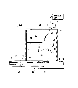
Fig. 1 is a schematic side view showing a first
preferred embodiment of the invention. The optical
digitizer implemented in this embodiment comprises a
transparent flat plate 10 of plastic etc. forming a light
active surface located above a graphic recording medium
20, and a cursor 100 functioning as an optical reader or
an optical recognition device movably mounted on the flat
plate 10. The transparent flat plate 10 comprises light
emitting media e.g. fluorescent media arranged so as to
form a predetermined coordinate correlatvie pattern 12.
More particularly, the coordinate correlative pattern 12
is described on or in the flat plate 10 with a fluorescent
paint diffused into transparent polymer. The graphic
recording medium 20 may be a paper sheet on which figures
or characters labelled 22 are described.
The optical recognition device 100 as the cursor
has a hollow casing member 110 serving as a black box with
respect to an optical system assembled therein, which will
be described later. The casing member 110 has an opening
opposite the sur-face of the flat plate 10. A transparent
positioning arm 112 extending in a lateral direction is
provided on the outer periphery of the casing member 110.
The positioning arm 112 is provided in the middle position
thereof with a crucial mark 114. The provision of the
positioning arm 112 allows an operator to visually trace a
-- 10 --
75S3
graphic data location on the recording medium 20 in
accordance with a movement of the cursor 100, thus to
effect positioning of the cursor 100 with respect to the
graphic data location.
The optical recognition device 100 further
comprises an optical system 120 assembled within the
casing member 110. The optical system 120 comprises a
light source 122, a first optical filter 124 positioned
between the light source 122 and the pattern 12 of the
flat plate 10, and a light focusing convex lens 126 and a
second optical filter 128 which are positioned between the
pattern 12 of the flat plate 10 and a sensor unit to be
referred to soon. These members 122, 124, 126 and 128
constituting the optical system will be described later in
greater detail.
The optical recognition device 100 further
compises a sensor unit 130 having a two-dimensional CCD
~charge coupled device) assembled within the casing member
110, a switch 140 provided on the casing member 110, a
first signal line cable 142 connecting the sensor unit 130
to the switch 140, and a second signal line cable 144
connecting the switch 140 to a graphic data processor
200. Thus, the sensor unit 130 is operative to sense
light emitted from a partial pattern which falls within a
predetermined limited visual range of the coordinate
correlative pattern 12 to produce a corresponding electric
signal, thereby effecting computation based on the
~7SiS3
elect:ric signal in the graphic data processor to determine
position coordinates of the graphic data on the coordinate
medium. The above mentioned crucial mark 114 is provided
for positioning a certain figure 22 (a qraphic data)
described on the paper sheet 20 when visually tracing
figures 22 in order to obtain graphic information of the
figures 22~ In the embodiment, the flat plate 10 is
placed on the paper sheet 20 on which figures 22 to be
inputted are drawn. Thus, the position coordinates at a
point 22P of a figure 22 is determined by moving the
cursor 100 on the flat plate 10 so that the point 22P of
the figure 22 is in register with the crucial mark 114 of
the positioning arm 112 provided on cursor 100. Such a
positioning viewed from the upward direction is shown in
Fig. 2 wherein an indication of the pattern 12 is omitted
for eliminating complexity.
A method of determining position coordinates on
the flat plate 10 indicative of the point 22P will be
described below. As previously described, the optical
system 120 provided within the hollow casing member 110 as
the black box is provided with the light source 122. The
light source 122 may be a light source which emits a
substantially monochromatic light having a luminance peak
at a wavelength of ~0. A characteristic curve a in
Fig. 3 indicates a spectrum of light irradiated from such
a light source 122. For instance, a light emitting diode
of GaP (gallium-phosphorus) may be used as the light
lZ~SS3
source 122. The ]iyht emitting diode of GaP has a
luminance peak at a wavelength of 555 nm (nano meter).
Light irradiated from the light source 122 passes through
the first optical filter 124 having a transmission
characteristic as indicated by a characteristic curve b in
Fig. 4 (e.g. a characteristic to cut off light having a
wavelength longer than 570 nm when the above-mentioned LED
is used) to irradiate the flat plate 10 having the pattern
12 and the paper sheet 20 positioned below. In view of
the above nature, the first optical filter 124 will be
referred to as a short-pass filter hereinafter. As
described above, the pattern 12 is described with a
fluorescent paint which has a peak of optical energy
absorption at a wavelength of ~0 to emit a fluorescence
having a peak at a wavelength ~ o) based on the
absorbed optical energy. A characteristic curve c in Fig.
3 shows a spectrum of such a fluorescence. By way of
example, Rhodamine B may be used as the fluorescent paint,
which has a pealc of absorption at a wavelength of 550 to
560 nm, and a luminance peak of the output fluorescence at
a wavelength of about 590 nm. In this embodiment, most of
components of wavelength ~0 of the light are reflected
at white portions on the paper sheet 20 where figures 22
are not drawn. On the other hand, most of components of
wavelength ~0 of the ]ight are absorbed at black
portions where figures 22 are drawn. The second optical
filter 128 has a transmission characteristic as indicated
l~';/SS;3
by d in Fig. 4 (e.g. a characteristic to cut off light of
a wavelenyth shorter than 570 nm when the above-mentioned
LED and Rhodamine B are used). In view of the above
nature, the second optical filter 128 will be referred to
as a short cut fllter thereinafter. It is apparent from
this characteristic that light which has passed through
the filter 124 and then has been scattered and reflected
within the black box 110 is cut off by the filter 128,
with the result that the light does not arrive at the CCD
sensor unit 130. In contrast, SinCQ the fluorescence
having the wavelength ~1 emitting from the pattern 12
passes through the filter 128 via the convex lens 126,
only the pattern 12 is projected as a positive image on
the CC~ sensor unit 130. The requirement of the pattern
12 drawn with a fluorescent paint on the flat plate 10 is
as follows. When optically recognizing a partial pattern
which falls within a limited visual range of the pattern
12, an arbitrary pattern may be used as far as position
coordinates in the center of the partial pattern and a
rotational angle of the visual range can be calculated.
Fig. 5 shows a partially enlarged view of an
example of the pattern 12, e.g., a lattice pattern. The
spacings between longitudinal lines and those between
lateral lines are set at a multiple of integer of unit
length e.g. 1 mm. Apparently, these lines are drawn at
random. It is now assumed that binary digits ("1" and
"0") are assigned to respective coordinate locations
- 14 -
lZ975S3
corresponding to the multiple of integer of 1 mrn in the
longitudinal and lateral directions of the lattice pattern
depending upon whether the longitudinal and lateral lines
are present or absent at the respective coordinate
locations, thus to express the respective coordinate
locations by code sequence. In this embodiment, code
sequence of the above nature may be M-sequence (maximum
period sequence). Such M-sequence can be created by means
of a circulating shift register as shown in ~ig. 6. The
circulating shift register comprises four stage cascade
connected J-K flip-flops 60 to 63, an AND gate 64, an
inverter 65, and a clock feed line 67. The M-sequence
output from the AND gate 64 is defined by repetition of a
bit pattern having a fifteen-bit length as expressed by
110110010100001. This sequence is characterized in that
successive four bits are different from each other,
respectively. Namely, when a selection of successive four
bits in order from the leftmost bit of the above-metioned
bit sequence is made to obtain fifteen kinds of four bit
codes different from each other, as indicated by (1101),
(1011), (0110), (1100), (1001), (0010), (0101), (1010),
(0100), (1000), (0000), (0001), (0011), (0111), and
(1110). In general, the M-sequence created by N stages of
shift registers are defined by repetition of a bit pattern
having (2N-l) bit length, thus creating (2 -1) kinds
of four successive N bit codes different from each other.
By making use of this nature of the M-sequence, it is
- 15 -
~3'7SS~
possible to obtain position coordinates and a rotational
angle of the black box 110 on the flat plate 10 in
accordance with a method described below. In Fig. 5, a
square 14 as indicated by a dotted line shows an example
of a visual range of the black box 110 projected on the
two-dimensional CCD sensor unit :L30. From a partial
pattern which falls within the visual range, it is
possible to calculate position coordinates and a
rotational angle of the center 16 of the visual range 14.
Namely, first is to find out an arbitrary single straight
line from a patial pattern reac by the two-dimensional CCD
sensor unit 130. In this instance, it is possible to
calculate an angle ~ of the straight line with respect to
a longitudinal or lateral line within the visual range 14
with ease. Second is to calculate spacings between
longitudinal lines and these between lateral lines within
the visual range 14, thereby to determine a corresponding
successive four bit code of the M-sequence, thus
determining a section or division to which the center 16
belongs. Precise position coordinates of the center 16
within the center 14 are determined by calculating
distances from the center 16 to the respective nearest
longitudinal and lateral lines. Since the distance from
the center 16 within the visual range 14 of the sensor
unit 130 to the crucial mark 114 is a constant value which
can be known in advance, it is possible to easily obtain
position coordinates from the above distance, the
- 16 -
~37~5~3
rotational angle ~ and the position coordinates of the
center 16. The above-mentioned calculation is executed by
the graphic data processor 200 connected to the black box
110 through the cable 144. Such a processing is
periodically effected only for a time period during which
the cables 142 and 144 are electrically connected by the
switch 140.
Then, a second preferred embodiment of an optical
digitizer according to the present invention will be
described with reference to Fig. 7. The elementary
configuration of this embodiment is similar to that of the
first-mentioned embodiment. This embodiment is
characterized in that a set of light sources 122A and 122B
irradiating light fluxes having the same wave length ~2
are provided instead of the single light source 122, in
that a set of short-pass filters 124A and 124B having an
optical characteristic to allow light having a wavelength
~ 3 ( ~ ~2) to pass therethrough are
provided instead of the single cut-pass filter 124, in
that a semiconductor memory 132 is added to temporarily
store image information sensed by the sensor unit 130, and
in that fluorescent paint for the pattern 12 emitting
fluorescent light having a wavelength longer than ~4
( > ~3) is used.
An image of a partial pattern which falls within
a predetermined visual range of the pattern 12 focused on
the sensor unit 130 through the convex lens 12~ and the
- 17 -
~Z~ 53
short-cut filter 128 is sensed by the sensor uni-t 130 as a
positive image. Thus, information of the partial pattern
corresponding thereto is stored in the semiconductor
memory 132. The information of l:he image temporarily
stored in th semiconductor memory 132 is fed to the
graphic information processor 200 (not shown herein) via
the cable 144, and then the information is processed
therein in a manner similar to the method as described in
the first embodiment.
As stated above, the novel optical digitizer
according to the present invention can realize size
reduction, improvement of accuracy and elimination of
influence of electromagnetic noise.
- 18 -